Abstract
The anodization of Ti° enables the formation of well-ordered TiO2 nanotubes, a highly promising nanomaterial with exceptional photochemical properties and potential applications in the energy and environmental sectors. This study addresses the growth of TiO2 nanotubes on large-scale surfaces applied for photocatalytic processes. The present investigation approaches the scaling up of the reactor for anodizing Ti°-coated flat surfaces and thus connecting the TiO2-nano-structure with real-world applications. For this, 316 stainless steel sheets were coated with a uniform Ti° layer using the arc cathodic method. The results indicate that the (~3 µm) thick Ti° arc-PVD coatings are well anodized, despite the inherent amount of µm-sized droplets produced during the deposition. The results reported here highlight the effects of the anodization process parameters—voltage, current, and time—on nanotube growth. At 60 V, the nanotubes exhibited a highly uniform cylindrical morphology, homogeneous walls contributing to an ordered, stable, and open nanostructure at large Ti-coated surfaces. The scaling up of the reactor for the controlled anodization process of Ti° coating is addressed. This approach validates Ti°-based PVD coatings at a semi-industrial scale on commercial stainless steel, thus enabling affordable production costs. Lastly, the anodization of Ti° coatings is a viable, scalable manufacturing process for producing photocatalytic nanostructured surfaces.
1. Introduction
Controlled manufacturing of nanostructures has emerged as a promising area in nanotechnology over the last few years. The development of materials with enhanced properties and new functionalities has driven a revolution across fields, such as energy, medicine, electronics, and the environment. Among these materials, titanium dioxide (TiO2) has become one of the most studied compounds due to its exceptional physicochemical and photochemical properties, low cost, widespread availability, and non-toxic nature. Its strong oxidation potential, high chemical resistance, and structural stability make it a versatile material with various environmental applications, ranging from photocatalytic processes for water treatment [1] to solar cells for clean energy production (e.g., photo-splitting, photo-reforming of organics) [2] to environmental gas sensors [3].
Within the vast field of TiO2 research, the growth of self-organized structures, such as TiO2 nanotubes, has gained particular attention due to their unique properties: a high surface-to-volume ratio, enhanced electron-transfer efficiency, and the associated photocatalytic activity arising from the intrinsic band gap of TiO2. The formation of TiO2 nanotubes depends heavily on the fabrication methods employed, which is advantageous because these procedures are relatively simple and do not require specialized nanoscale techniques. The ability to synthesize well-defined nanotubular structures through controllable anodization processes has driven the development of new methodologies to improve the textural, morphological, and crystalline properties of TiO2, with an emphasis on promoting the formation of the anatase phase, which is recognized for its high photocatalytic activity [4].
Among various fabrication methods, electrochemical anodization has emerged as one of the most effective techniques for modifying the surfaces of metals or semiconductor substrates, generating functional or protective oxide layers. The anodization of Ti° is a well-known process that has been investigated worldwide by various research groups. This process involves using a conductive Ti anode, while a noble or inert conductive metal (e.g., platinum foil and stainless-steel foil or sheet) serves as the cathode. During the anodization, the application of a constant or variable voltage in an appropriate electrolyte [i.e., ethylene glycol + water + ammonium fluoride (NH4F)] promotes the formation of the porous TiOx layer, where nanopores and nanotubes develop through the ionic transport of F− and the migration of Ti4+ and O2− species. The final morphology of the nanotubes is determined by several process parameters, such as the applied voltage, the electrolyte used, the F− concentration, temperature, and the anodizing time [5,6,7]. These structural features are crucial for performance in catalytic and photocatalytic applications: arrays with increased length and specific area favor pollutant adsorption and degradation [7,8,9].
In contrast, a perpendicular orientation and optimized length are preferable for photoelectrochemical applications aimed at hydrogen production [10,11]. Diameter and wall engineering facilitates the incorporation of co-catalysts and metals for CO2 reduction [12] or selective reactions [13,14] and the controlled presence of defects and dopants improves visible response and carrier separation [15,16], thus expanding the usefulness of nanotubes in environmental and energy processes. The growth of long TiO2 nanotubes is strongly influenced by the use of fluoride-containing electrochemical processing agents in combination with a high viscosity electrolyte [7]. Fluoride ions (F−) are crucial in the anodization mechanism, as they modulate oxide dissolution and promote the self-organization of TiO2 nanostructures. Depending on the F− concentration, the anodization process can produce compact oxide films, ordered nanotubes, or porous layers. While the length of the nanotubes is primarily determined by the anodization time, the tube diameter increases linearly with the applied potential [7,17]. Under typical conditions (fluoride-containing electrolyte, applied potentials of 10–60 V, and room temperature), titanium surfaces develop arrays of amorphous TiO2 nanotubes [18,19]. Post-anodization heat treatment is required to achieve crystallinity in air at 350–550 °C; generally, this results in anatase, while higher annealing temperatures can introduce partial or complete transformation to rutile, with the final phase composition determined by the annealing temperature, duration, and atmosphere [19].
Most investigations into the development of TiO2 nanotubes are conducted on a small-scale laboratory level. However, to apply such nanostructures in real-world applications, it is urgent to scale up the anodization process to larger surfaces and geometries without compromising their morphological and functional properties. Scaling-up the process poses challenges, including structural uniformity, mechanical stability, and temperature control [20]. Recent studies have shown that increasing the substrate area affects nanotube morphology, reducing their height and increasing the separation between them, especially at the edges. Some of the most relevant lines of progress include: (i) controlling electrolyte behavior through the use of conditioned or “ages” electrolytes and regulating their temperature to maintain stable conductivity and F- dissolution capacity during extended anodization [21,22,23], (ii) active thermal management of the bath (electrolyte circulation and cooling) to minimize thermal gradients that cause local variations in the dissolution rate and consequently, in the length and uniformity of the nanotubes [22,24], (iii) optimizing the geometry and configuration of the electrochemical system (anode-cathode design, electrode spacing, sample arrangement and even bipolar anodization for 3D structures) to homogenize the electric field and current distribution over large areas [8,9], (iv) electrolyte modification by high viscosity additives to control ionic transport and reduce local turbulence during growth [25], and (v) application of conformal coating (e.g., ALD) or post-anodization surface treatments that improve the mechanical and thermal stability although sometimes at the cost of a slight loss of active area [26,27]. In this regard, several studies have explored the synthesis of nanotubular TiO2 in larger surface areas. For example, the use of an ethylene glycol-based electrolytic solution containing fluorides to anodize pure titanium plates of approximately 10 cm2, applying voltages between 20 and 60 V for 2 h at ~25 °C. They reported the formation of nanotubes with external diameters between 80 and 120 nm and lengths up to 4 µm, depending on the anodization time [28]. Similarly, an electrolyte composed of 98% ethylene glycol, 2% deionized water and 0.3% by weight of NH4F, very similar to the electrolyte used in the present work, was used to anodize Ti foils at 60 V for 1–2 h at a controlled temperature of ~30 °C with constant stirring; they produced nanotubes with 100 nm diameters and lengths up to 3 µm [6]. In addition, nanotubes with external diameters of ~100 nm and lengths of 1.8–2.9 µm were obtained by anodizing a 64 cm2 area using an electrolyte containing on ethylene glycol, NH4F, and phosphoric acid and applying 40 V for 2 h with stirring at 23 °C [9]. Finally, the scaling of the anodizing process of titanium plates, using an electrolyte of similar composition (ethylene glycol, 0.5% NH4F, 2% water), applying 60 V, and maintaining the distance between the anode and cathode constant at 30 mm, resulted in nanotubes with diameters between 100 and 150 nm and lengths close to 3 µm [17]. However, all these investigations indicate that as the anodized surface area increases, maintaining morphological uniformity and growth homogeneity becomes more challenging, particularly due to electrolyte density and localized heating. These advances in developing TiO2 nanotubes over larger areas highlight the potential of these nanostructures for practical applications; however, further investigation is needed to fully scale up the anodization process to exploit their catalytic activity.
For these reasons, the present investigation explores the growth of TiO2 nanotubes using thin Ti° coatings deposited by the semi-industrial arc-PVD method on commercially available 316 stainless steel (SS) sheets or quartz plates and using the same SS as a cathode material, thus paving the way for large-scale production of Ti°-coatings for nanostructuring. This investigation aims to produce TiO2 nanotubes for photocatalytic systems.
2. Materials and Methods
2.1. The Ti° Coating Deposition Process
The Ti° coating was deposited on as-received (Ra = 94 nm) and mirror-polished (Ra = 11.7 nm) stainless steel flat samples of 10 × 50 mm with a thickness of 1 mm, 50 × 50 × 1 mm, and on 30 × 30 mm quartz glass surfaces. Other substrate geometries were also explored; however, in the following, the investigation reported here refers only to the flat surfaces. The Ti°-coating was deposited using a semi-industrial PVD DOMINO Mini system from Oerlikon Balzers Coating Germany GmbH, Bergisch Gladbach, Germany. This system is equipped with 4 cathodic arc sources, a 3-axis rotation system, and an effective coating volume of 330 mm Ø × 400 mm, with a load capacity of 120 kg. Figure 1 displays the fixation arrangement of the steel sheet samples. The sample size is only limited by the effective coating volume. A commercial Ti° target with a diameter of 100 mm and 99.5% purity (Plansee Composite Materials GmbH, Lechbruck am See, Germany) was used for coating deposition. The stainless-steel sheets were mounted on a double-rotation system and heated to ~450 °C for 2 h in a vacuum chamber at 10−5 mbar. Prior to Ti° coating deposition, the plates were activated via the AEGD (Arc-Enhanced Glow Discharge) cleaning process (erosion with Ar+ ions), with an RF polarization of −250 V at 20 kHz. Finally, the Ti° coating was deposited using an arc-source and the arc-PVD method, with a current of 150 A, a flow rate of 500 sccm of pure Ar, and a duration of ~1 h, under a pressure-controlled condition during the coating deposition of 10−2 mbar. The same coating procedure was used for Ti coating deposition on the quartz substrates.
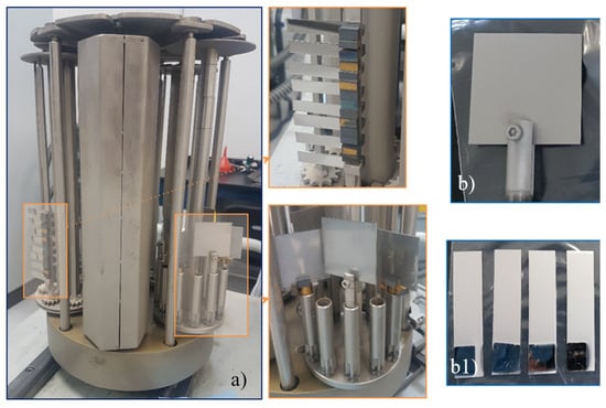
Figure 1.
Stainless steel sheets fixed at a three-axis rotation system prior to the deposition of metallic Ti° (a), & Ti° deposited by the arc PVD coating method on 50 × 50 mm (b) and 10 × 50 mm (b1) stainless steel sheets.
2.2. Synthesis—Electrochemical Anodization of Ti° Coating
TiO2 nanotubes (TNTs) were synthesized by electrochemical anodization. An electrolyte solution was prepared consisting of 98% vol. ethylene glycol (C2H6O2), 2% vol. deionized water (H2O), and 0.3% weight NH4F. First, NH4F was dissolved in water to obtain a homogeneous solution; then ethylene glycol was added under constant stirring at 120 rpm, and the mixture was maintained until the electrolyte became transparent and uniform. The same concentration was applied in all anodization experiments. The 10 × 50 × 1 mm SS sheets were anodized using a 50 × 50 × 1 mm counter electrode of the same SS material in a 250 mL glass container. According to the electrode disposition, the distance between the anode and cathode was ~25 mm in a 150 mL glass container. The 50 × 50 × 1 mm SS sheets were applied to understand the scalability of the anodization process. In this case, the distance between the electrodes was ~40 mm and remained constant within a 600 mL glass container. Table 1 summarizes the anodization conditions of the Ti° arc-PVD coatings. This table displays the set-point values for the current and the applied voltage during anodization. These process variables were fixed at the potentiostat at the beginning of the anodization. The voltage was maintained at the set point value, while the current was automatically adjusted during anodization. The current dropped to a very low value (in the mA range) due to the isolating TiOx layer formed during the process. A DC power supply of 32 V and 3 A from GW INSTEK GPE-2323 was applied for these experiments.

Table 1.
The anodizing set-point parameters for the Ti° arc-PVD coatings.
Based on the anodization results obtained in these two beaker configurations, the design of tubular anodization reactors with fixed geometries and electrode configurations was carried out to guarantee the reproducibility and scalability of the process. The first tubular reactor (TR1) was designed and manufactured using a commercial PVC tube with ∅ = 47.8 mm and a length of 20.3 mm. The electrolyte volume was ~36 cm3. The anodization conditions for this reactor were 60 V and 0.04 A for 1 h. The anodized area was 0.7853 cm2, and the current density was 50 mA/cm2. The current was selected based on the initial anodization experiments conducted in the reagent glass. The temperature was not controlled, and no cooling was applied during the anodization, which was performed in a single-batch, non-stirred regime in the tubular reactor TR1. The images of this anodization reactor are shown in Figure 2, where (a) depicts the design of the tubular configuration, (b) illustrates the anodization process carried out inside the PVC chamber, and (c) presents Ti°-coated quartz substrates before and after anodization. These images confirm that the TR1 reactor maintains electrolyte confinement and enables reproducible nanotube growth on the Ti° coatings.
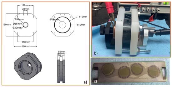
Figure 2.
(a) Design of the tubular anodizing reactor, (b) anodization process of Ti° arc PVD coatings in the tube PVD reactor of lengths = 20.3 mm and ∅ = 47.8 mm. (c) Ti°-coated quartz substrates and anodized sections.
In the second tubular reactor (TR2), TNTs were grown on a flat Ti° substrate surface measuring 30 × 30 mm. This reactor has a capacity of ~415 cm3 for electrolyte, where the diameter was 115 mm and the length was 40 mm. In this tubular reactor design, the operating conditions were modified to promote nanotube growth using thick Ti° coatings. The anodization conditions were 60 V and 0.46 A for 2 h. Under these conditions, the anodization area was 9.62 cm2, giving a current density of ~50 mA/cm2; this is a proportional increase factor of 12.25 compared to the anodizing area in TR1, with the same anodization current and no cooling or stirring applied. The images of the reactor design and a representative anodization result in TR2 are shown and discussed in the following sections.
2.3. The TiO2-Nanotubes—Ti° Coating System Analysis
The chemical composition and the micro- and nanostructure of the as-deposited Ti arc-PVD coatings and the anodized surfaces were analyzed on a Field Emission Scanning Electron Microscope FE-SEM from JEOL (Tokyo, Japan) JSM 7200F equipped with an Ultim Max 100 EDS detector from Oxford Instruments. For EDS-mapping analysis the AZtec Software (https://www.aztecsoftware.com) was used. The crystalline phases of the metallic Ti° coatings and anodized systems were analyzed in a SmartLab XRD diffractometer from Rigaku in PB/PSA mode (Parallel Beam/Parallel Slit Analyzer) with a low incidence angle (ω = 2.5°) using Cu Kα radiation (40 kV, 44 mA) at a step size of 0.02°. The diffraction patterns were indexed using the PDXL 2 Software from Rigaku Version 2.3.1.0.
The average roughness (Ra) of the Ti°-coated surfaces was measured using a DektakXT profilometer from Bruker, with Stylus tip of 12.5 μm radius over a 2 mm distance, and repeated several times.
3. Results
3.1. The As-Coated State of the Ti° Arc-PVD Coating
3.1.1. Microstructure, Chemical Composition; And Crystalline Phases of the Anodized arc-PVD Ti°-Coating
In the initial state, the Ti° arc PVD microstructure displayed a Ra = 0.297 ± 0.02 μm, which is roughly 2 times smaller than the Ra = 0.613 ± 0.24 μm of the initial surface of the commercially available SS sheet. The Ra slightly increases after coating deposition in mirror-finished SS samples, whereas in unpolished steel, the Ti°-roughness decreases, suggesting that mirror polishing of the SS is unnecessary when applying the arc-PVD deposition method, as the Ti° coating compensates for the SS manufacturing finishing roughness. As a reference, the microstructure of the unpolished SS surface prior to the Ti°-coating is shown in the SEM-images of Figure 3(a,a1). The microstructure of the as-deposited Ti° arc-PVD coatings is displayed in Figure 3(b,b1), and the crystalline state of the Ti° layer is displayed in Figure 3c. Only the hexagonal characteristic phase textured in the (101) planes of Ti was observed. These FE-SEM images highlight the sizes and shapes of the Ti°-droplets (sizes slightly < 1 μm and up to 2 to 3 μm) that belong to the characteristic surface microstructure of the arc-PVD process.
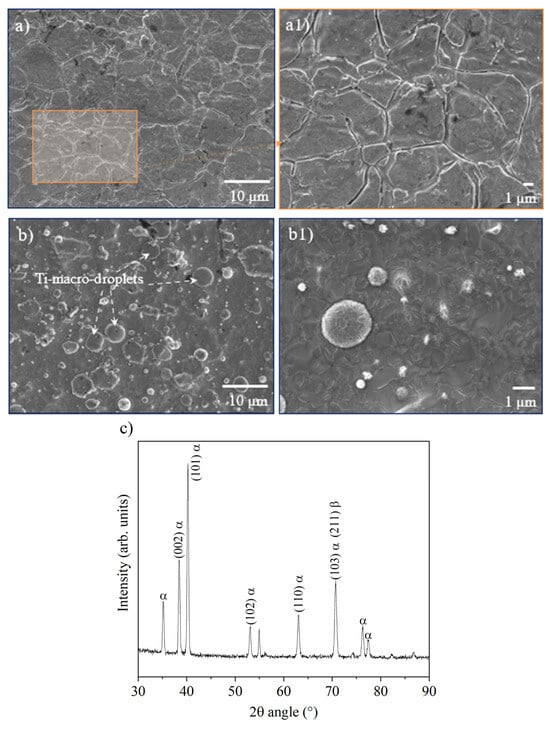
Figure 3.
(a,a1) images of the initial surface state of the stainless-steel sheet, (b,b1) the as-coated state of the Ti° deposited by the arc-PVD method, and (c) crystalline state of the as-deposited Ti° arc-PVD.
3.1.2. Beaker Anodization of Ti° by Arc PVD
The first series of anodization experiments was carried out on 10 × 50 SS sheets coated with Ti° using a set voltage of 30 V, a current flow of 3 A, and an anodization time of up to 120 min. The maximum current started at ~50 mA/cm2 and, after a few minutes, stabilized at ~40 mA/cm2 in all anodization experiments. Figure 4a–d display the anodized Ti° coating surface under these conditions. The TNTs exhibit a cylindrical morphology with open pores and thin walls, with the internal diameters slightly exceeding 100 nm. The TNTs formed after a 30 min anodization period; see the inset SEM image in Figure 3a, which shows nanotubes with internal diameters close to 30 nm. Under these anodization conditions, open nanotubes are difficult to find because a dense top layer (< 100 nm) covers the top ends of the TNTs.
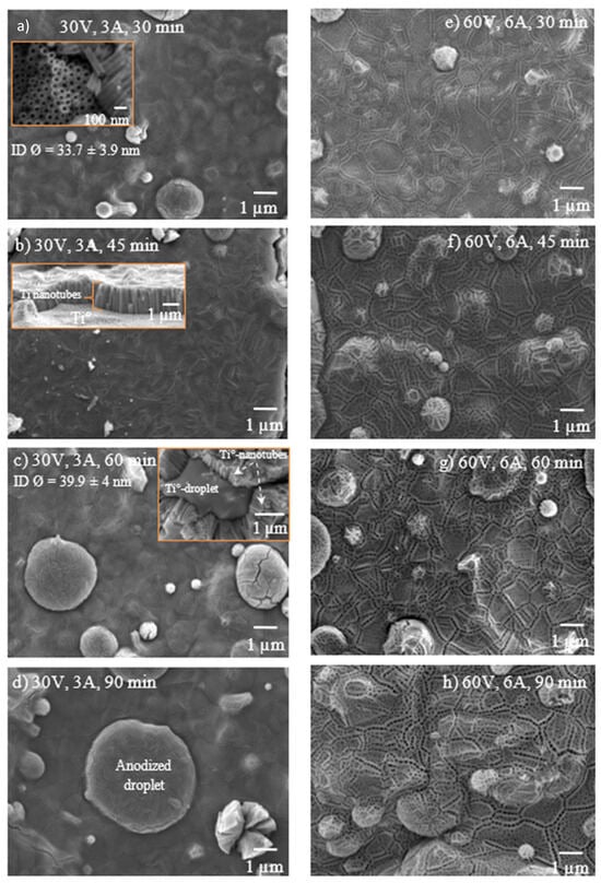
Figure 4.
The effect of voltage, current, and time on the anodized surface of Ti arc-PVD coatings, (a–d) 30 V & 3 A, (e–h) 60 V & 6 A.
Few sections are exposed due to stresses that produce cracks and spallation of the TNTs at the interface with the Ti°-surface, see inset SEM images in Figure 4b,c. Chemical mapping of such regions allows identifying the Ti° surface and the boundary to the TiOx nanotubes. The anodized layer also contained F, which comes from the electrolyte. These results also indicated that no cross-contamination was caused by the use of the SS as a counter electrode (Figure 5). At a synthesis time of 60 min and an applied voltage of 30 V, an increase in both the length (~1.1 µm on average) and diameter (~40 nm) of the TNTs is observed. However, the results are not entirely satisfactory due to material agglomeration and the formation of a non-uniform TiOx film, resulting in thickness variations. These effects are markedly observed in the counter-surface of the Ti°-droplets. The top layer that covers nanotube openings is observed even after 90 min of anodization. This top layer also reveals the grain boundaries of the initial Ti°-crystals deposited by the arc-PVD method. Very similar effects on the quality of the anodized Ti°-surface are observed upon treatment applying 60 V and 6 A up to 90 min (Figure 4e–h).
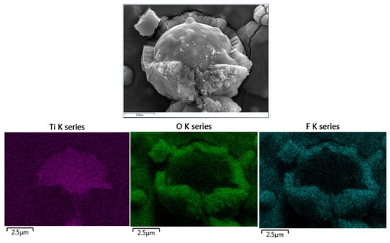
Figure 5.
Elemental mapping for TiOx nanotubes.
The TNTs are revealed in large-scale regions of the anodized Ti-surfaces only after 2 h of anodization at 60 V and 6 A; see Figure 6b. The zoomed regions in 6b1 & 6b2 showed the anodized surface and the mean internal diameter calculated from using ImageJ Software 2025 version, respectively. The SEM analysis shows that the growth of the TiOx oxide on the Ti°-coated surface is highly homogeneous, with some agglomerations that do not detach or spall. The TNTs exhibit a cylindrical morphology with open pores and thin nanoscale walls, with the internal diameter of these nanostructures slightly exceeding 100 nm; see the micrographs obtained after anodization at 60 V for 90 min. The anodizing process conditions significantly influence the morphology and topography of the TNTs. Factors such as internal diameter, wall thickness, and nanotube length are highly dependent on the synthesis conditions [3]. When a voltage is applied, the TiOx oxide layer thickness increases over time, thereby decreasing the electric field. In this scenario, the electric field is proportional to the thickness, making the process self-limiting. The nanotube length is determined by the anodizing time, while the applied voltage and anodizing time linearly control the diameter.
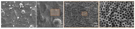
Figure 6.
(a) Large-scale anodization of Ti arc-PVD coatings, 60 V, 6 A, and 120 min thermal treatment-free, (b) with thermal treatment, (b1) zoom in the anodized surface & (b2) mean internal diameter = 124 ± 13.6 nm and length = 157 nm calculated from using ImageJ software.
Based on the results discussed in the previous paragraphs, it was evident that electrochemical anodization successfully produces open tubular nanostructured oxides by applying the 10 × 50 mm Ti°-coated SS-substrates. Therefore, the anodized plate area was increased to a Ti°-coated 50 × 50 mm SS-substrate to evaluate the extrapolation of the process to larger Ti°-coated surfaces. The anodization process was carried out under the synthesis conditions that yielded the best results (60 V, 2 h) for the smaller Ti-coated substrates. By applying the same anodization conditions and increasing the area of the Ti°-coated anode, the anodized film did not reproduce the same morphological characteristics. This discrepancy may be attributed to variations in the current density, as the total current intensity is distributed over a larger surface area while the anodizing parameters remain unchanged. These observations led us to partially conclude that, to scale up the anodizing process successfully, it is essential to fix the anodization parameters, such as current density, to maintain the same electrochemical conditions and guarantee reproducibility (e.g., electrode distance between the anode and cathode, area of the exposed electrodes, current density). Alternatively, modifications in electrolyte concentration and anodizing time may be required to compensate for the decrease in surface area, which determines the current flowing during the nanostructuring process. These results show that a slight variation in the anodization process may be sufficient to reproduce the nanostructuring of the Ti° arc PVD coatings fully. Based on this information, the design of an anodization reactor was undertaken and discussed in the following sections.
3.2. The XRD Analysis of the TNTs
The X-ray diffraction (XRD) analysis of the Ti° before the anodization process reveals peaks corresponding exclusively to the hexagonal crystalline Ti° phase (JCPDS 00-044-1294); this is confirmed by the most intense diffraction peak at 2θ = 40.171°, corresponding to the (101) planes of the hexagonal crystal structure. This data indicates that the as-deposited Ti° coating is crystalline and in its α-phase, which is thermodynamically stable at room temperature. The XRD analysis revealed that the initially obtained TiOx anodized layers are fully amorphous (Figure 7). No diffraction peaks from the SS substrate were identified. The amorphous nature of the TNTs has been previously demonstrated by several authors [29,30,31,32]. Subsequently, a thermal treatment at 500 °C was performed, promoting the crystallization of the amorphous TiOx layer into crystalline TiO2. The resulting diffractogram displays characteristic peaks of the anatase phase of TiO2 for the (101), (112), and (220) planes at 2θ = 25.27°, 38.257°, and 70.49°, respectively (JCPDS 00-064-0863). The heat treatment facilitated the TiO2 crystallization by preserving the nanotube morphology.
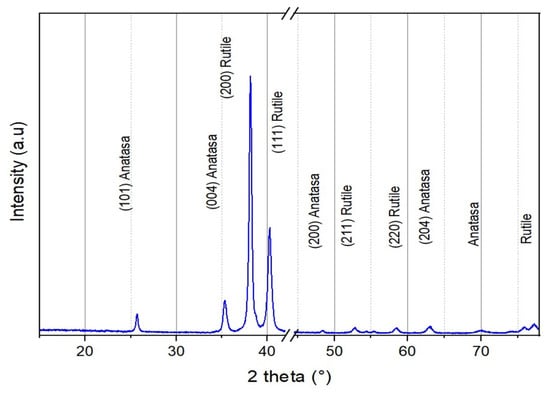
Figure 7.
XRD data of the TiO2-nanotubes after thermal treatment at 500 °C/2 h.
During heating, the supplied thermal energy enabled atomic rearrangement within the initial amorphous structure, promoting the nucleation and growth of crystalline domains within the TNTs without compromising their nanostructural integrity. This phenomenon allowed for the transition to a stable anatase phase while maintaining the tubular architecture and preserving the high aspect ratio and specific surface area. The structural stability of the nanotubes under thermal treatment suggests that diffusion and recrystallization occurred in a controlled manner, preventing sintering and structural collapse.
3.3. Scaling up the Anodization Process of Ti°-Coatings
In TR1, anodized surfaces with a diameter of 1 cm are generated on the Ti°-coated surface by cathodic arc PVD (Figure 8). The SEM images confirm nanotube growth with cylindrical morphology and open porosity (a1 & a2). This area is insufficient if the aim is to assess the reactive capacity of the Ti° coating in photocatalytic processes. However, it was the first step in identifying the main variables that allow the reactor to be scaled up and the material to be generated with the area necessary to develop the photocatalysis process.
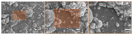
Figure 8.
Nanotubes obtained with a tubular reactor ~0.8 in length and a commercial tube of ∅ = 2, thermal treatment-free. (a) Large-scale anodization of Ti arc-PVD coatings, 60 V, 0.4 A, and 1 h. (a1) and (a2) zoom in on the anodized surface.
For TR2, variables included the initial area obtained, the desired final area, the previous current intensity, and the desired current intensity. From these values, the area ratio index and the current required for the new cell were obtained. With this information, it was possible to scale up a reactor that generated an approximate anodized area of 1 cm2 on a glass surface coated with Ti° in arc PVD to an anodized area of 10 cm2, maintaining a voltage of 60 V and changing the current intensity from 0.2 A to 0.46 A (Figure 9). The images show (a) the design of the TR2 reactor, (b) the anodization process in operation, and (c) Ti°-coated substrates before and after anodization. The uniform color change and surface modification confirm the reproducibility of nanotube growth at larger scales.
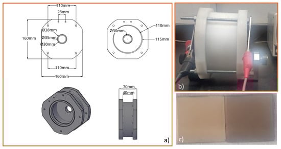
Figure 9.
(a) Reactor design TR2, (b) Ti° arc PVD coating anodizing process, and (c) Ti-coated substrates before (left) & after anodization (right). The anodization area = 30 × 30 mm.
The calculated electrical power is 12 W and 27.6 W, respectively; this provides information about energy consumption, since, theoretically, the power increases by almost double from TR1 to TR2, yet in both cases, the energy consumption is considered low. From this point of comparison, the energy expenditure is exploited in the second reactor, where the scaling was carried out, since anodized films with the capacity to develop applications such as photocatalysis can be obtained, a characteristic not present in the anodized films obtained in the first reactor. It is important to note that a larger initial volume of electrolyte solution is required. However, increasing the volume also increases the reuse period of the solution, reducing reagent costs and extending its life across more anodizing process cycles on different substrates. The electrolyte degradation under these anodization conditions still needs to be evaluated. As shown in Figure 10, the TR2 configuration enabled anodization over an area of 30 × 30 mm, producing homogeneous nanotube layers across the entire substrate, as confirmed by SEM zoom images (Figure 10(a1)) showing well-ordered nanotubes with open porosity.
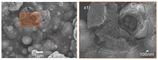
Figure 10.
TiOx nanotubes obtained with the TR2 reactor design for anodization of Ti°-coating on 30 × 30 mm SS substrates without thermal treatment. (a) Large-scale anodization of Ti arc-PVD coatings, 60 V, 0.46 A, 2 h. (a1) Zoom in on the anodized surface.
4. Discussion
The results demonstrate that the initial roughness of the stainless-steel substrate does not determine the final surface properties of the arc-PVD Ti° coating, since the coating compensates for the substrate finishing. The microstructure and surface characteristics of the Ti° coating are defined by the arc-PVD method itself. This finding implies that mirror polishing of stainless steel is unnecessary prior to deposition, which is advantageous for large-scale applications as it reduces costs and preparation time. Similar observations were reported in other studies, in which PVD coatings were found to homogenize substrate topographies regardless of initial roughness [8,9]. In the beaker anodization experiments, nanotube growth was limited by a compact top layer, which disappeared only after extended anodization times and higher voltages. This behavior aligns with previous reports showing that both anodization time and applied potential are critical parameters for determining nanotube length and diameter [6,17]. For example, Gong et al. [6] reported comparable effects of prolonged anodization in ethylene glycol-based electrolytes, highlighting that incomplete dissolution of the oxide barrier can hinder the formation of open pores. Furthermore, the anodization of the arc-PVD microstructure indicated that previous finishing and polishing steps might reduce stresses, cracks, and damage in some sections; this might be particularly important for thick TiOx nanotubes on micrometer-sized Ti-droplets, which are typical of the arc-PVD deposition process.
When scaling anodization from small (10 × 50 mm) to larger (50 × 50 mm) substrates, nanotube morphology was not reproduced under identical conditions. This discrepancy can be attributed to variations in current density: as the anodized area increases, the effective current per unit surface decreases, thereby altering local electrochemical conditions. Maintaining constant current density and electrode geometry is therefore essential to ensure reproducibility at large scales. This conclusion is consistent with recent studies that emphasize that reactor design, electrode spacing, and electrolyte management strongly affect nanotube homogeneity over large areas [8,20,22,24]. Structural analysis further confirmed that the as-anodized TiOx layers are amorphous, while annealing at 500 °C induces crystallization into anatase, with partial rutile formation. Notably, the nanotubes retained their tubular architecture after thermal treatment, indicating that recrystallization occurs in a controlled manner without sintering or collapse. These observations are consistent with prior work reporting that annealing between 350 and 550 °C promotes anatase formation while maintaining structural integrity [18,19].
Regarding scalability, the TR1 tubular reactor enables nanotube growth over small areas (~1 cm2), which was sufficient to identify the key operating variables. The TR2 design, in contrast, enabled homogeneous nanotube formation on 30 × 30 mm substrates by adjusting the current intensity from 0.2 A to 0.46 A while maintaining 60 V. Although energy consumption doubled between TR1 and TR2, it remained low in both cases, confirming the efficiency of the process. Additionally, the larger electrolyte volume required in TR2 can be reused in multiple anodization cycles, thereby reducing reagent costs. These findings validate the scalability of anodizing Ti° arc-PVD coatings and highlight reactor design as a decisive factor for achieving reproducible nanotube morphology.
Altogether, this study demonstrates that semi-industrial Ti° coatings can be reliably anodized to form well-ordered nanotube arrays, providing a scalable, cost-effective route toward photocatalytic surfaces. These insights help bridge the gap between laboratory-scale anodization and real-world applications, paving the way for larger TiO2 nanotube modules in environmental and energy technologies.
5. Conclusions
The Ti° coating was successfully deposited on 316 SS substrates using the semi-industrial arc-PVD process, forming a uniform layer with characteristic microstructural features, including micrometer-sized droplets. Subsequent electrochemical anodization at 60 V for 2 h yielded highly ordered TiO2 nanotube arrays, promoting the self-organized formation of open nanotubes and nanoporous structures in both droplet-free flat regions and atop Ti° droplets. Cracks and partial detachment of nanotube sections were occasionally observed on larger droplets, suggesting that the size and curvature of these micrometer-scale features play a critical role in maintaining nanotube adhesion. Notably, the nanotubes retained their morphology and open porosity after thermal treatment at 500 °C, which promoted the coexistence of stable anatase and rutile phases.
In addition, the TR1 reactor design enabled the growth of nanotubes on arc-PVD Ti° coatings deposited on metallic and quartz substrates with minimal electrolyte consumption. At the same time, the TR2 configuration ensured reproducible anodization on 30 × 30 mm quartz substrates, demonstrating the scalability of the nanostructuring process. Taken together, these findings provide valuable insights into the anodization parameters of Ti°-coated surfaces and establish a practical route toward process standardization, ultimately facilitating the development of larger TiO2 nanostructured modules for real-world applications.
Author Contributions
Conceptualization, G.C.M.-R. and R.H.-A.; methodology and investigation, G.C.M.-R., R.H.-A., N.C.A.D.P. and A.M.E.-M.; Analysis formal, G.C.M.-R. and N.C.; resources, G.C.M.-R. and R.H.-A.; writing—original draft preparation, G.C.M.-R., R.H.-A., N.C.A.D.P. and A.M.E.-M.; funding acquisition, G.C.M.-R. and R.H.-A. All authors have read and agreed to the published version of the manuscript.
Funding
The research for this publication has been supported by the Science and Technology Institute of Michoacan ICTI-PICIR-22-047-C, Coordination of Scientific Research CIC-UMSNH-2024-2025, SEP-CONACYT-ANUIES-ECOS NORD-322574, and M22P01 projects.
Data Availability Statement
The data presented in this study are available on request from the corresponding author.
Conflicts of Interest
The authors declare no conflicts of interest.
References
- Horikoshi, S.; Serpone, N. Can the photocatalyst TiO2 be incorporated into a wastewater treatment method? Background and prospects. Catal. Today 2020, 340, 334–346. [Google Scholar] [CrossRef]
- Chiarello, G.L.; Dozzi, M.V.; Selli, E. TiO2-based materials for photocatalytic hydrogen production. J. Energy Chem. 2017, 26, 250–258. [Google Scholar] [CrossRef]
- Zakir, O.; Ait-Karra, A.; Idouhli, R.; Khadiri, M.; Dikici, B.; Aityoub, A.; Abouelfrida, A.; Outzourhit, A. A review on TiO2 nanotubes: Synthesis strategies, modifications, and applications. J. Solid State Electrochem. 2023, 27, 2289–2307. [Google Scholar] [CrossRef]
- Zakir, O.; Idouhli, R.; Elyaagoubi, M.; Khadiri, M.; Aityoub, A.; Koumya, Y.; Rafqah, S.; Abouelfida, A.; Outzourhit, A. Fabrication of TiO2 Nanotube by Electrochemical Anodization: Toward Photocatalytic Application. J. Nanomater. Onlinelibr. Wiley 2020, 2020, 4745726. [Google Scholar] [CrossRef]
- Dubey, R.S. Synthesis and characterization of titania nanotube arrays by electrochemical method for dye sensitized solar cells. Arch. Appl. Sci. Res. Sch. Res. Libr. 2013, 5, 28–32. Available online: https://www.scholarsresearchlibrary.com/articles/synthesis-and-characterization-of-titania-nanotube-arrays-by-electrochemical-method-for-dye-sensitized-solar-cells.pdf (accessed on 5 September 2025).
- Gong, D.; Grimes, C.A.; Varghese, O.K.; Hu, W.; Singh, R.S.; Chen, Z.; Dickey, E.C. Titanium oxide nanotube arrays prepared by anodic oxidation. J. Mater. Res. 2001, 16, 3331–3334. [Google Scholar] [CrossRef]
- Macak, J.M.; Aldabergerova, S.; Ghicov, A.; Schmuki, P. Smooth anodic TiO2 nanotubes: Annealing and structure. Phys. Status Solidi (a) 2006, 203, R67–R69. [Google Scholar] [CrossRef]
- Sopha, H.; Baudys, M.; Sepúlveda, M.; Rusek, J.; Hromadko, L.; Rodriguez-Pereira, J.; Krysa, J.; Macak, J.M. Gas phase photocatalysis on large-scale TiO2 nanotube layers for pollutant degradation: Influence of the nanotube crystallinity. ACS Appl. Nano Mater. 2023, 6, 17053–17059. [Google Scholar] [CrossRef]
- Szkoda, M.; Trzciński, K.; Zarach, Z.; Roda, D.; Łapiński, M.; Nowak, A.P. Scaling Up the Process of Titanium Dioxide Nanotube Synthesis and Its Effect on Photoelectrochemical Properties. Materials 2021, 14, 5686. [Google Scholar] [CrossRef]
- Roy, P.; Berger, S.; Schmuki, P. TiO2 Nanotubes: Synthesis and Applications. Angew. Chem. Int. Ed. 2011, 50, 2904–2939. [Google Scholar] [CrossRef]
- Albu, S.P.; Ghicov, A.; Macak, J.M.; Schmuki, P. 250 µm long anodic TiO2 nanotubes with hexagonal self-ordering. Phys. Status Solidi (RRL)-Rapid Res. Lett. 2007, 1, R65–R67. [Google Scholar] [CrossRef]
- Chen, X.; Mao, S.S. Titanium Dioxide Nanomaterials: Synthesis, Properties, Modifications, and Applications. Chem. Rev. ASC Publ. 2007, 107, 2891–2959. [Google Scholar] [CrossRef] [PubMed]
- Wei, L.; Yu, C.; Zhang, Q.; Liu, H.; Wang, Y. TiO2-based heterojunction photocatalysts for photocatalytic reduction of CO2 into solar fuels. J. Mater. Chem. A 2018, 6, 22411–22436. [Google Scholar] [CrossRef]
- Chen, S.-A.; Nian, J.-N.; Tsai, C.-C.; Teng, H. TiO2 Nanotube-Supported Cu as the Catalyst for Selective NO Reduction with NH3. J. Air Waste Manag. Assoc. 2012, 57, 600–605. [Google Scholar] [CrossRef]
- Luttrell, T.; Halpegamage, S.; Tao, J.; Kramer, A.; Sutter, E.; Batzill, M. Why is anatase a better photocatalyst than rutile?-Model studies on epitaxial TiO2 films. Sci. Rep. 2014, 4, 4043. [Google Scholar] [CrossRef]
- Liu, N.; Schneider, C.; Freitag, D.; Hartmann, M.; Venkatesan, U.; Müller, J.; Spiecker, E.; Schmuki, P. Black TiO2 Nanotubes: Cocatalyst-Free Open-Circuit Hydrogen Generation. Nano Lett. 2014, 14, 3309–3313. [Google Scholar] [CrossRef]
- Zhuang, Y.; Li, P.; Qin, L.; Zhang, S.; Chen, B.; Zhu, Y.; Wang, B.; Zhu, X. Real role of fluoride ions in the growth of anodic TiO2 nanotubes. J. Phys. Chem. C Nanomater. Interfaces 2024, 128, 5741–5748. [Google Scholar] [CrossRef]
- Sopha, H.; Baudys, M.; Hromadko, L.; Lhotka, M.; Pavlinak, D.; Krysa, J.; Macak, J.M. Scaling up anodic TiO2 nanotube layers–Influence of the nanotube layer thickness on the photocatalytic degradation of hexane and benzene. Appl. Mater. Today 2022, 29, 101567. [Google Scholar] [CrossRef]
- Varghese, O.K.; Gong, D.; Paulose, M.; Grimes, C.A.; Dickey, E.C. Crystallization and high-temperature structural stability of titanium oxide nanotube arrays. J. Mater. Res. 2003, 18, 156–165. [Google Scholar] [CrossRef]
- Sulka, G.D.; Kapusta-Kołodziej, J.; Brzózka, A.; Jaskuła, M. Anodic growth of TiO2 nanopore arrays at various temperatures. Electrochim. Acta 2013, 104, 526–535. [Google Scholar] [CrossRef]
- Guo, T.; Ivanovski, S.; Gulati, K. Tuning electrolyte aging in titanium anodization to fabricate nano-engineered implants. Surf. Coat. Technol. 2022, 447, 128819. [Google Scholar] [CrossRef]
- Mohan, L.; Dennis, C.; Padmapriya, N.; Anandan, C.; Rajendran, N. Effect of Electrolyte Temperature and Anodization Time on Formation of TiO2 Nanotubes for Biomedical Applications. Mater. Today Commun. 2020, 23, 101103. [Google Scholar] [CrossRef]
- Suhadolnik, L.; Marinko, Ž.; Ponikvar-Svet, M.; Tavčar, G.; Kovač, J.; Čeh, M. Influence of Anodization-Electrolyte Aging on the Photocatalytic Activity of TiO2 Nanotube Arrays. J. Phys. Chem. C 2020, 124, 4073–4080. [Google Scholar] [CrossRef] [PubMed]
- Szaniawska-Białas, E.; Brudzisz, A.; Nasir, A.; Wierzbicka, E. Recent Advances in Preparation, Modification, and Application of Free-Standing and Flow-Through Anodic TiO2 Nanotube Membranes. Molecules 2024, 29, 5638. [Google Scholar] [CrossRef]
- Ocampo, R.A.; Echeverría, F.E. The Effects of Anodization Conditions on TiO2 Nanotubes Features Obtained Using Aqueous Electrolytes with Xanthan Gum. Inventions 2023, 8, 109. [Google Scholar] [CrossRef]
- Zazpe, R.; Prikryl, J.; Gärtnerova, V.; Nechvilova, K.; Benes, L.; Strizik, L.; Jäger, A.; Bosund, M.; Sopha, H.; Macak, J.M. Atomic Layer Deposition Al2O3 Coatings Significantly Improve Thermal, Chemical, and Mechanical Stability of Anodic TiO2 Nanotube Layers. Langmuir ASC Publ. 2017, 33, 3208–3216. [Google Scholar] [CrossRef]
- Ng, S.; Sopha, H.; Zazpe, R.; Spotz, Z.; Bijalwan, V.; Dvorak, F.; Hromadko, L.; Prikryl, J.; Macak, J.M. TiO2 ALD Coating of Amorphous TiO2 Nanotube Layers: Inhibition of the Structural and Morphological Changes Due to Water Annealing. Front. Chem. 2019, 7, 38. [Google Scholar] [CrossRef]
- Macak, J.M.; Tsuchiya, H.; Taveira, L.; Aldabergerova, S.; Schmuki, P. Smooth Anodic TiO2 Nanotubes. Angew. Chem. Int. Ed. 2005, 44, 7463–7465. [Google Scholar] [CrossRef]
- Gönüllü, Y.; Haidry, A.A.; Saruhan, B. Nanotubular Cr-doped TiO2 for use as high-temperature NO2 gas sensor. Sens. Actuators B Chem. 2015, 217, 78–87. [Google Scholar] [CrossRef]
- Wang, Z.; Chen, K.; Xue, D. Crystallization of amorphous anodized TiO2 nanotube arrays. RSC Adv. 2024, 14, 8195–8203. [Google Scholar] [CrossRef]
- Park, I.J.; Kim, D.H.; Seong, W.M.; Han, B.S.; Han, G.S.; Jung, H.S.; Yang, M.; Fan, W.; Lee, S.; Lee, J.-K.; et al. Observation of anatase nanograins crystallizing from anodic amorphous TiO2 nanotubes. CrystEngComm 2015, 17, 7346–7353. [Google Scholar] [CrossRef]
- Stiller, M.; Barzola-Quiquia, J.; Esquinazi, P.; So, S.; Hwang, I.; Schmuki, P.; Böttner, J.; Estrela-Lopis, I. Electrical transport properties of polycrystalline and amorphous TiO2 single nanotube. Nano-Struct. Nano-Objects 2017, 10, 51–56. [Google Scholar] [CrossRef]
Disclaimer/Publisher’s Note: The statements, opinions and data contained in all publications are solely those of the individual author(s) and contributor(s) and not of MDPI and/or the editor(s). MDPI and/or the editor(s) disclaim responsibility for any injury to people or property resulting from any ideas, methods, instructions or products referred to in the content. |
© 2025 by the authors. Licensee MDPI, Basel, Switzerland. This article is an open access article distributed under the terms and conditions of the Creative Commons Attribution (CC BY) license (https://creativecommons.org/licenses/by/4.0/).