Abstract
To decrease the complexity and increase the efficiency of wireless power transfer (WPT) systems, this paper proposes a novel self-excited invert rectification method for the design of the invert rectifier of the receiver (Rx). The self-excited invert rectifier can perform the self-driving and soft-switching of the MOSFETs as well as the frequency-tracking function without a microcontroller. This allows us to greatly simplify the structure of the invert rectifier and increase the transfer efficiency (TE) of the WPT system. Firstly, a self-excited invert rectifier circuit is designed, and a self-excited invert rectification method is studied. Additionally, the power loss of the self-excited invert rectifier is analyzed. Finally, the self-excited invert rectifier of the WPT experimental system is designed. The self-excited invert rectification method is then verified. The key component parameters of the self-excited invert rectifier are provided and optimized. The TE of the WPT system that includes the self-excited invert rectifier is improved by more than 5% without a microcontroller. The self-excited invert rectifier of the Rx provides a practical solution for decreasing the complexity and increasing the TE of the WPT system.
1. Introduction
Tesla conducted a WPT experiment in the early 20th century [1]. WPT technology then made great progress [2,3]. In recent years, it has been widely used in many fields, including car mobile phones, electric vehicles, and mobile robots [4,5,6].
A WPT system typically contains AC power and a resonant system containing a transmitter (Tx), receiver (Rx), and rectifier [7]. The design of the rectifier is usually based on the full-bridge rectifier. The system has high efficiency. However, its structure is complex [8,9,10]. Ref. [11] introduced right-half-plane zeros into small-signal transfer functions to resolve the current source nature of the series–series compensation. They proposed adopting a different rectifier configuration for the system. A novel single-phase bidirectional ac–dc WPT topology is proposed in [12]. It allows the drawbacks of matrix-converter-based topologies to be overcome while retaining the advantages of single-stage topologies. A bidirectional WPT system, which can function in both forward and reverse modes, was proposed in [13]. Ref. [14] proposed the LCC-S type compensation topology because magnetically coupled WPT systems face a wide input voltage range and variable load in some specific application scenarios, resulting in variable output voltage. Ref. [7] proposed a novel full-bridge step density modulation for WPT systems based on the step density averaging principle, which can achieve full-range ZVS operation. Ref. [15] proposed a new six-switch topology based on the full-bridge converter, which achieves the self-adaptation of a dynamic change in system parameters. According to the above references, full-bridge inverters are used to convert DC to AC with a microcontroller on the Tx side. Additionally, four rectifier diodes are usually used for full-bridge rectification on the Rx side.
However, in the WPT research community, self-excited inverters are usually used on the Tx side. Ref. [16] used a self-excited inverter to construct the inversion stage of the WPT system without a PWM generator and a microcontroller, which greatly simplified the hardware structure. In addition, soft-switching (SS) and automatic frequency tracking (FT) can be performed without requiring additional control strategies, which also reduces the complexity. Ref. [17] proposed a self-excited inverter to obtain high-frequency AC power, which reduced the complexity of their WPT system. Additionally, the output voltage of the parallel–series WPT system with a self-excited inverter is resistant to load changes. An improved self-excited resonant circuit was also provided using a fully controlled low-power switch instead of a diode; the SS performance was improved, the temperature of the switch tube was reduced by about 7 °C, and the TE was also improved by about 4% [18]. The principle of a self-excited push–pull oscillation circuit was analyzed [19]. In a WPT system with a self-excited converter, the influence mechanism of magnetic shielding on the TE was analyzed; the optimal shielding distance was obtained [20]. These references indicate that self-excited inverters have a lot of excellent characteristics, such as SS, FT, the constant voltage output, etc. Thus, a method of the invert rectifier of the Rx is proposed by using the method and characteristics of the self-excited inverter on the Tx side, which is used to convert AC to DC without a microcontroller.
In view of the aforementioned studies, this paper proposes a novel self-excited invert rectification method to design the invert rectifier of the Rx, in order to reduce the complexity and increase the transfer efficiency (TE) of the WPT system. The self-excited invert rectifier can perform the self-driving (SD) and SS of the MOSFETs as well as the FT function without a microcontroller. This greatly simplifies the structure of the invert rectifier, and increases the TE of the WPT system. Firstly, a self-excited invert rectifier circuit is designed, and a self-excited invert rectification method is studied. Additionally, the power loss of the self-excited invert rectifier is analyzed. Finally, the self-excited invert rectifier of the WPT experimental system is then designed. The self-excited invert rectification method is then verified. The key component parameters of the self-excited invert rectifier are provided and optimized. The TE of the WPT system, which includes the self-excited invert rectifier, is improved by more than 5% without requiring a microcontroller. The self-excited invert rectifier of the Rx provides a practical solution for reducing the complexity and increasing the TE of the WPT system. In contrast to the existing works, the contributions of this article are as follows:
- (1)
- A self-excited invert rectification method is proposed and applied to design the invert rectifier of the Rx.
- (2)
- The key component parameters of the self-excited invert rectifier are provided and optimized to improve the TE.
The remainder of this paper is organized as follows. Section 2 describes the self-excited invert rectifier circuit, and provides a brief analysis of the working principle of the self-excited invert rectifier. Section 3 gives the analysis of the power loss of the self-excited invert rectifier. Section 4 presents the experiment results. Finally, conclusions are drawn in Section 5.
2. Design of the Self-Excited Invert Rectifier Circuit
The self-excited invert rectifier consists of a circuit with a symmetric structure, which can perform the SD and SS of the MOSFETs as well as the FT function without a microcontroller and without requiring additional control strategies.
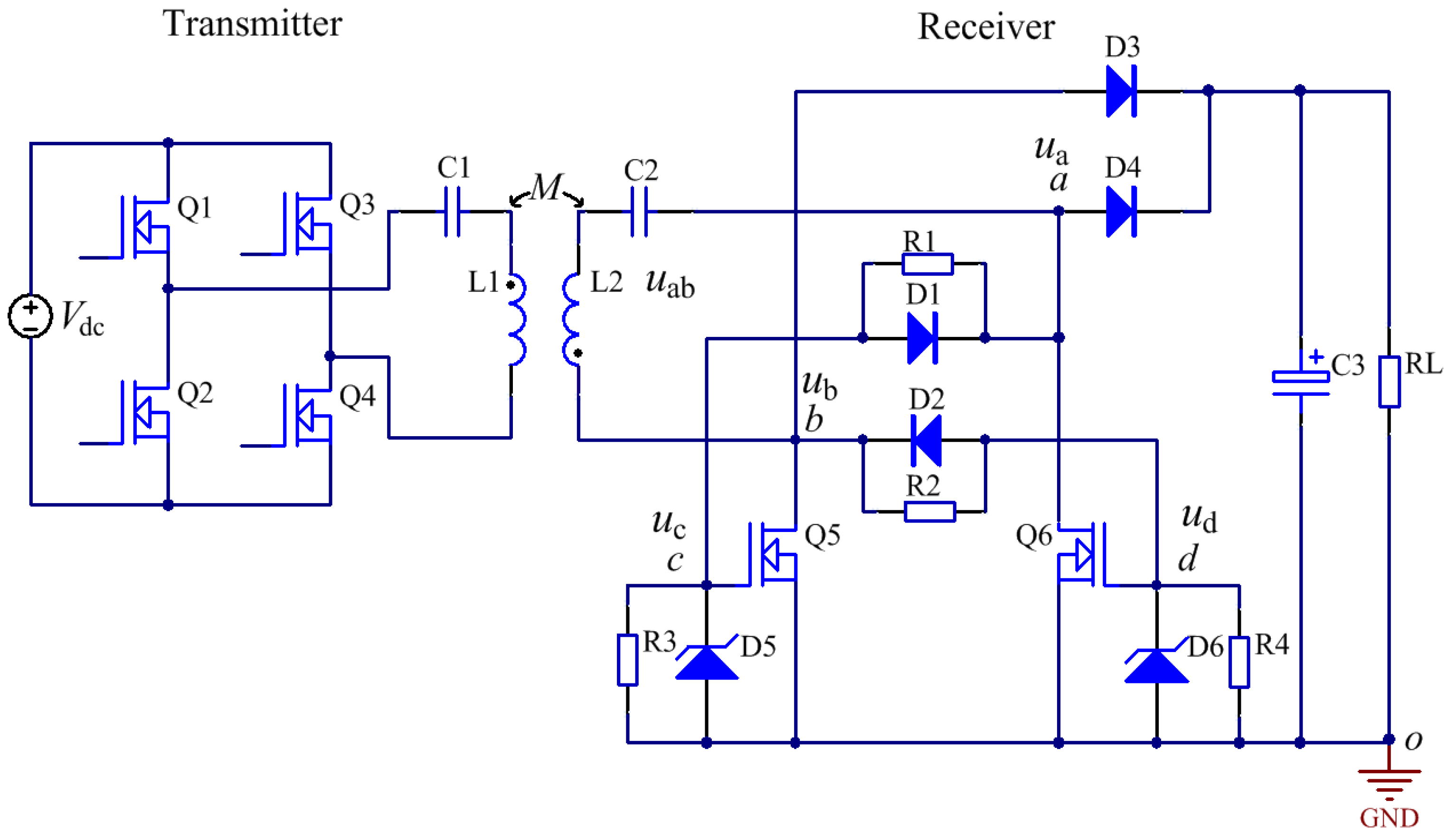
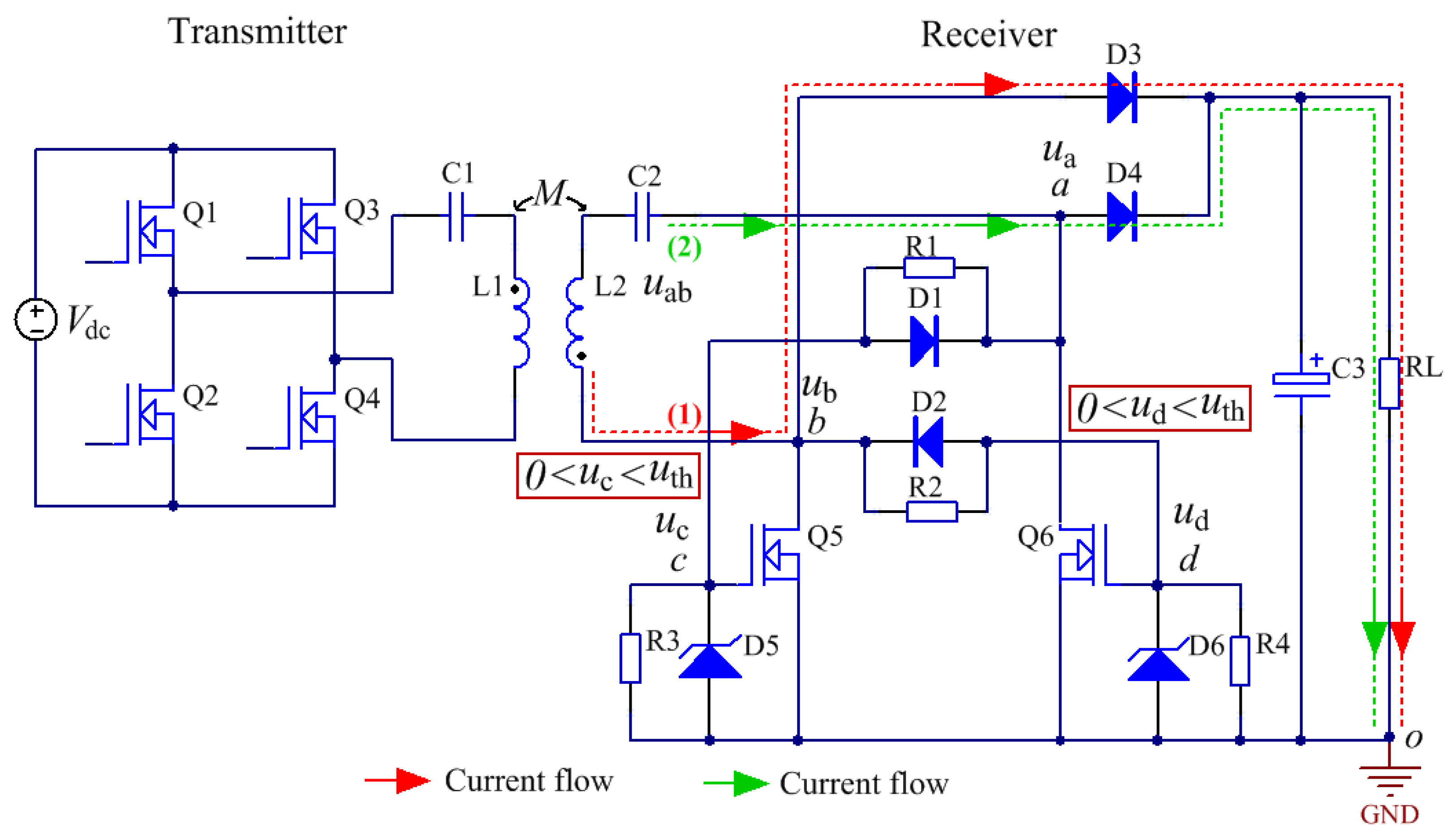
A diagram of the WPT system with the self-excited invert rectifier, which includes a Tx and an Rx, is shown in Figure 1. Q1–Q4 are the MOSFETs used as switching transistors in a full-bridge inverter, Vdc is the input power, L1 and L2 are the coils, C1 and C2 are the capacitors, M is the mutual inductance of L1 and L2, D1 and D2 are the fly-wheeling diodes, R1–R4 are the voltage divide resistors, D3 and D4 are the rectifier diodes, D5 and D6 are the Zener diodes which provide a stable voltage to protect the Q5 and Q6 MOSFETs used as switching transistors in the self-excited invert rectifier, C3 is the filter capacitor, RL is the load resistor, ua, ub, uc, and ud are the voltages of points a, b, c, and d, respectively, and uab is the voltage between points a and b. The parameters of the circuit of the WPT system are shown in Table 1.
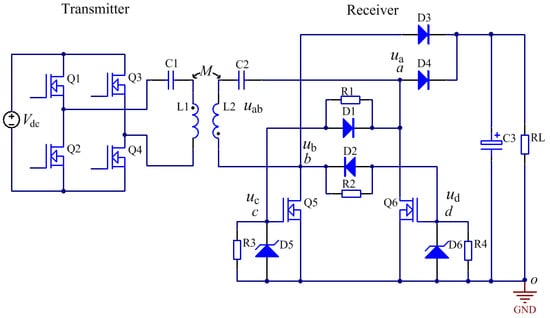
Figure 1.
WPT system with self-excited invert rectifier.

Table 1.
Parameters of the WPT system circuit with the self-excited invert rectifier.
According to Figure 1 and Table 1, the self-excited invert rectifier part only includes D1–D6, R1–R4, Q5, and Q6. The self-excited invert rectifier with a few components can perform the self-driving and soft-switching of the MOSFETs as well as the frequency-tracking function without a microcontroller. This allows us to greatly simplify the structure of the invert rectifier and increase the TE of the WPT system.
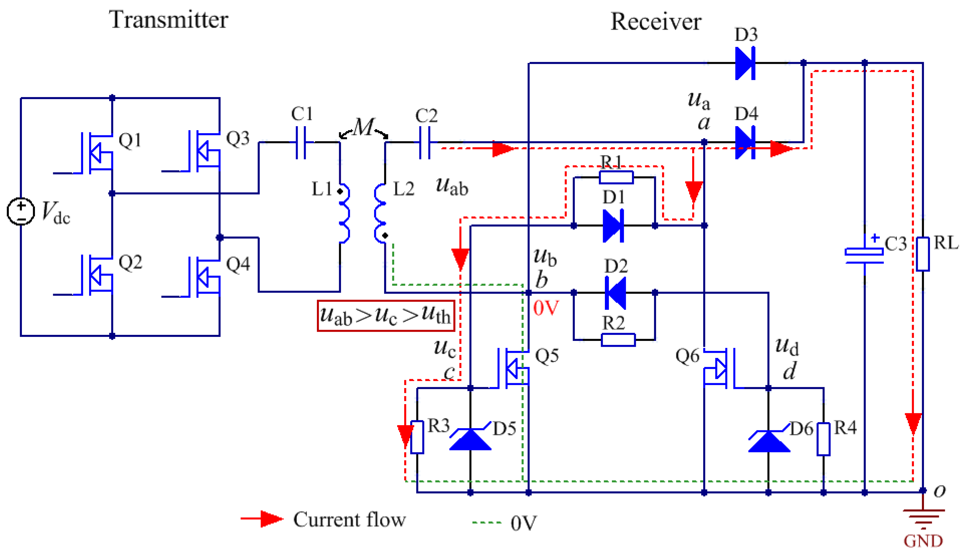
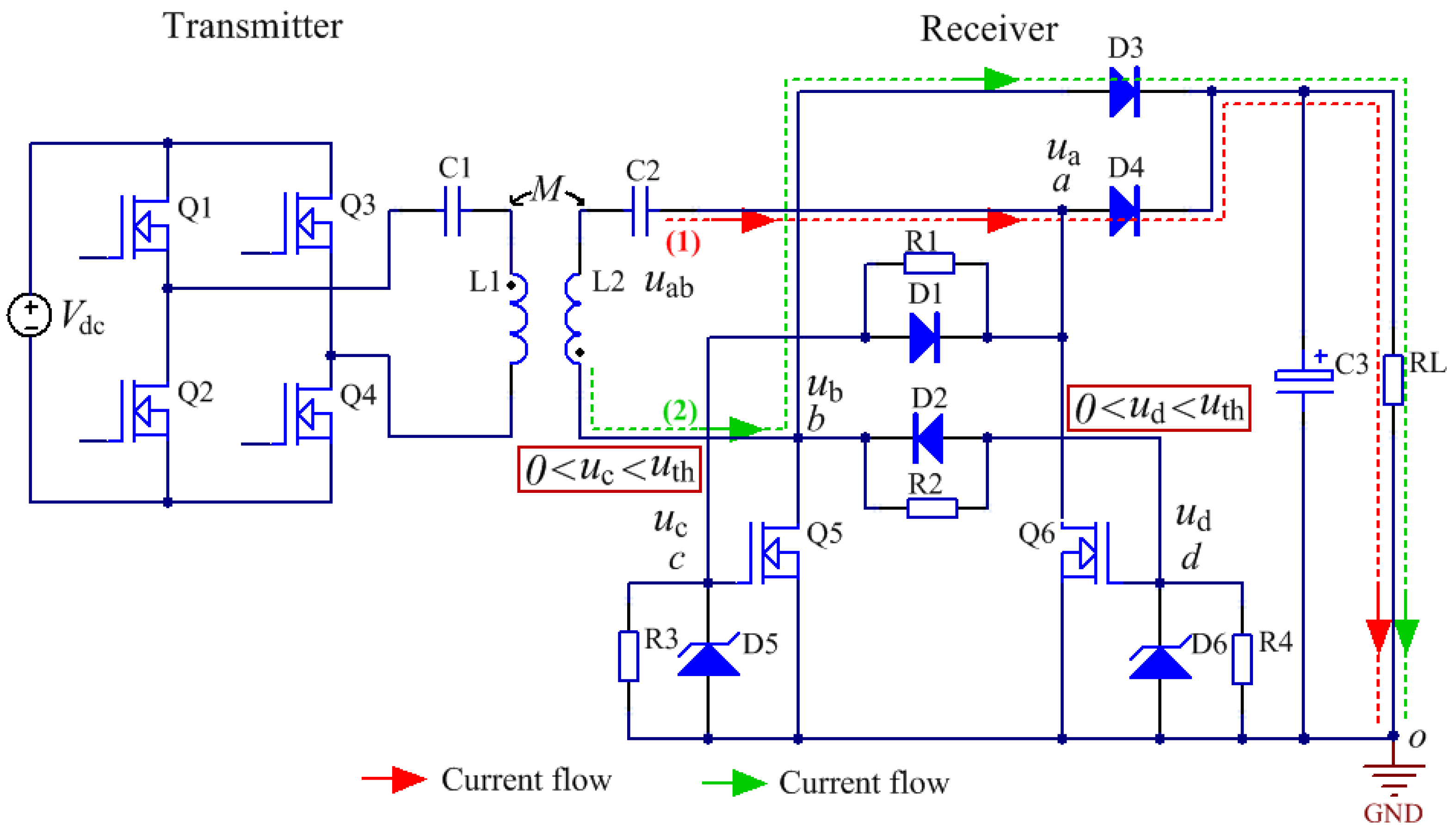
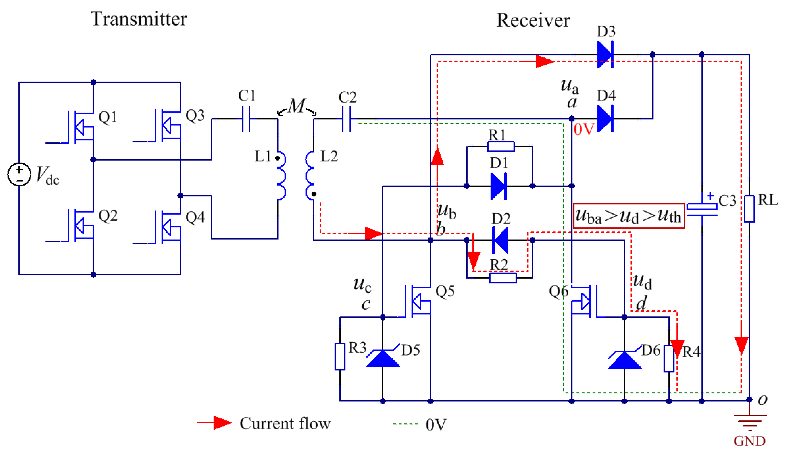
In the Rx, the self-excited invert rectifier consists of a circuit with a symmetric structure. The wireless power is transferred from the Tx to the Rx through magnetic coupling resonance. Under high-frequency sine voltage stimulation on the Rx side, because of the existence of R1–R4, Q5 and Q6 cannot simultaneously be in a blocked state nor in a conducting state. This indicates that at any moment, one MOSFET is on and the other one is off. A brief analysis of the working principle of the self-excited invert rectifier is then provided. According to this working principle, the self-excited invert rectifier is divided into four working modes. The obtained results are shown in Figure 2, Figure 3, Figure 4, Figure 5 and Figure 6. Assuming that at the beginning, Q5 is turned on while Q6 is blocked, the four working modes with uab = −uba, where Uth is the gate threshold voltage, are given as follows:
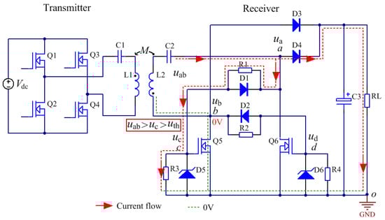
Figure 2.
Working mode 1 of the self-excited invert rectifier: Current flow is power and control loops; and 0 V is the same voltage level.
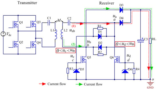
Figure 3.
Working mode 2 of the self-excited invert rectifier: Current flow of red dotted lines is the first process section; and Current flow of green dotted lines is the second process section.
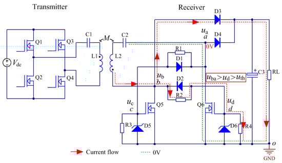
Figure 4.
Working mode 3 of the self-excited invert rectifier: Current flow is power and control loops; and 0 V is the same voltage level.
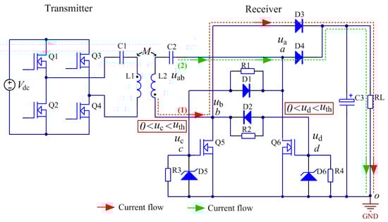
Figure 5.
Working mode 4 of the self-excited invert rectifier: Current flow of red dotted lines is the first process section; and Current flow of green dotted lines is the second process section.
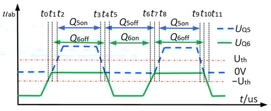
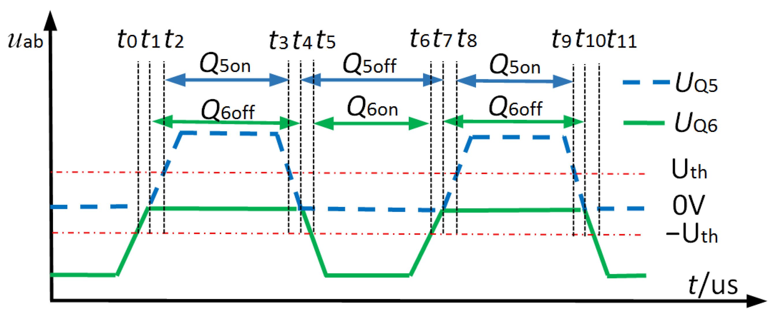
Figure 6.
Steady−state working waveform of the switching tubes in the self-excited invert rectifier.
(1) Mode 1: Based on Figure 2 and Figure 6, t2 and t3 are the on time of Q5 (i.e., Q5on time) and t1–t4 are the off time of Q6 (i.e., Q6off time). In other words, when uab increases from uc = Uth to the peak and then decreases to uc = Uth, Q5 is turned on while Q6 is blocked. The path of the current has two loops: power and control loops, (the red dotted lines in Figure 2). The power loop is from C2, point a, D4, and RL to point o, while the control loop is from C2, point a, R1, point c, and R3 to point o. Note that point o, Q5, point b, and the bottom of L2 have the same voltage level (0 V) (green dotted lines in Figure 2). In addition, R1 and R3 construct a voltage divider (VD) to provide bias voltage (BV) for Q5. Similarly, R2 and R4 construct a VD to provide BV for Q6. In this mode, Q5 is turned on because uab > uc > Uth. On the contrary, Q6 is blocked because ud = ub = 0 v. Thus, the invert rectifier circuit performs positive half-cycle rectification.
(2) Mode 2: According to Figure 3 and Figure 6, when the high-frequency sine voltage uab decreases from uc = Uth to zero, Q5 enters the amplification region from the conductive one at t3 and t4. Q5 is then blocked at time point t4 and time regions t4 and t7. In addition, when Q5 enters the amplification region and is blocked, the power is quickly released by a circuit loop of R2 and D2. This is the first process section (red dotted lines in Figure 3). On the other hand, the voltage is reversed at the next moment. When uba = −uab increases from zero to ud = Uth, Q6 enters the amplification region at the time regions t4 and t5. Q6 then turns on at the time point t5 and the time regions t5 and t6 when uba increases and ud > Uth. In addition, R2 and R4 construct a VD to provide BV for Q6, which remains turned on. This is the second process section (green dotted lines in Figure 3). Therefore, the invert rectifier circuit performs rapid switching of states.
(3) Mode 3: According to Figure 4 and Figure 6, t4–t7 are the off time of Q5 (i.e., Q5off time), and t5 and t6 are the on time of Q6 (i.e., Q6on time). In other words, when uba increases from ud = Uth to the peak and then decreases to ud = Uth, Q6 turns on while Q5 is blocked. The path of the current has two current loops: power and control loops (red dotted lines in Figure 4). The power loop is from L2, point b, D3, and RL to point o, while the control loop is from L2, point b, R2, point d, and R4 to point o. Note that point o, Q6, point a, and the right side of C2 have the same voltage (0 V) (green dotted lines in Figure 4). Moreover, R1 and R3 construct a VD to provide BV for Q5. Similarly, R2 and R4 construct a VD to provide BV for Q6. In this mode, Q6 is turned on because uba > ud > Uth. On the contrary, Q5 is blocked because uc = ua = 0 v. Therefore, the invert rectifier circuit performs negative half-cycle rectification.
(4) Mode 4: According to Figure 5 and Figure 6, when the frequency sine voltage uba decreases from ud = Uth to zero, Q6 enters the amplification region from the conductive region in the time regions t6 and t7. It is then blocked at the time point t7 and the time regions t7 and t10. In addition, when Q6 enters the amplification region and is blocked, the power is quickly released by a circuit loop of R1 and D1. This is the first process section (red dotted lines in Figure 5). On the other hand, the voltage is reversed at the next moment. When uab increases from zero to uc = Uth, Q5 enters the amplification region in the time regions t7 and t8. It then turns on at the time point t8 and the time regions t8 and t9 when uab increases and uc > Uth. In addition, R1 and R3 construct a VD to provide BV for Q5, which remains turned on. This is the second process section (green dotted lines in Figure 5). Therefore, the invert rectifier circuit also performs rapid switching of states.
It can be deduced from the aforementioned analysis that L2 and C2 comprise a series resonant tank, whose resonant frequency determines that of the sine voltage on the Rx side. Furthermore, the switching frequency of Q5 and Q6 and the rectification frequency of the rectifier diode are determined by the frequency of the sine voltage stimulation on the Rx side. More precisely, the function of automatic FT is performed, where R1–R4 play a crucial role. In addition, due to R1–R4, the self-excited invert rectifier performs the SD of MOSFETs during the inversion process without the need for the signal detector and microcontroller that are used in traditional rectifiers. This significantly reduces the complexity of the control and structure as well as the cost, and increases the TE of the WPT system. Furthermore, R1 and R3 construct a VD to provide BV for Q5. Similarly, R2 and R4 construct a VD to provide BV for Q6. Moreover, R1 and D1 construct a circuit loop and quickly release power when Q6 is blocked. Note that R2 and D2 have the same function. The two circuit loops provide a quick energy release channel, which accelerates the mode switching and reduces the power loss of Q5 and Q6. In addition, the product of Q5 and Q6 is AGM035N10A, which obtains 3 mΩ from the drain-source on-state resistor. It can reduce the power loss during the functioning of Q5 and Q6. Finally, D5 and D6 perform voltage stabilization to protect Q5 and Q6.
3. Analysis of the Power Loss of the Self-Excited Invert Rectifier
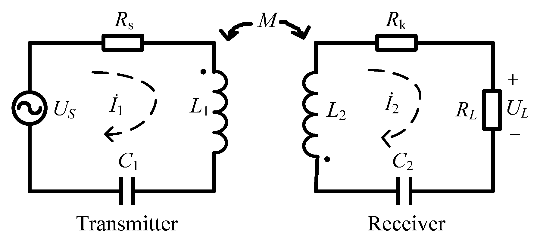
The circuits of the self-excited invert rectifier can be equivalent according to Figure 7. The circuit model has two resonant circuits, linked magnetically by mutual inductance M. US is the input power of the Tx; RS is the sum of the loss resistor and radiation resistor of the Tx; Rk is the sum of the loss resistor and radiation resistor of the Rx, which mainly includes the working resistors of Q5, Q6, D3, and D4; L1 and L2 are the inductors; C1 and C2 are the capacitors; RL is the load resistor; UL is the load voltage; and İ1 and İ2 are the currents of the Tx and Rx loops, respectively.
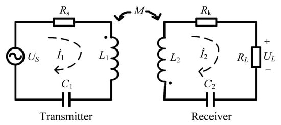
Figure 7.
Equivalent circuit of the WPT system with self-excited invert rectifier.
According to Figure 7, Kirchhoff’s voltage law, and angular frequency ω, the WPT system with the self-excited invert rectifier can be expressed as
The self-impedance values Z1 and Z2 are given by
The output power (OP) Pout can be given as [6]
where σ = RS/(Rk + RL) and β = RL/(Rk + RL) are the resistor ratios, R = Rk + RL is the resistor of the Rx side, τ = ωM/(RS(Rk + RL))0.5 is the impedance-coupled factor, and ξ is the frequency-detuning factor.
The TE η can be written as [6]
According to Equation (3), σ = RS/(Rk + RL), β = RL/(Rk + RL), and R = Rk + RL; when RS and Rk decrease, the OP Pout increases. According to Equation (4), β = RL/(Rk + RL), and τ = ωM/(RS(Rk + RL))0.5; when RS and Rk decrease, and ξ = 0, the TE η increases.
In summary, when RS and Rk decrease, the OP and TE improve. On the Rx side, the self-excited invert rectifier could reduce the value of Rk by decreasing the power losses of the MOSFETs (Q5 and Q6) and the forward voltage losses of the rectifier diodes (D3 and D4).
4. Experimental Results
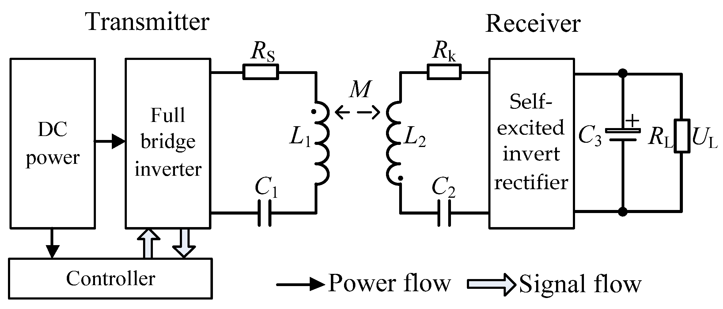
Figure 8 shows an experimental block diagram of the WPT system that includes a self-excited invert rectifier, where RS is the sum of the loss and radiation resistors of the Tx; Rk is the sum of the loss and radiation resistors of the Rx, which mainly includes the working resistors of Q5, Q6, D3 and D4; C3 is the filter capacitor; UL is the DC voltage of the load; and RL is the load resistor. Table 2 presents the parameters of the self-excited invert rectifier experimental equipment.
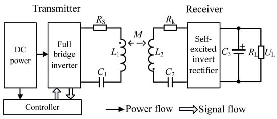
Figure 8.
Block diagram of the WPT system that includes a self-excited invert rectifier.
Table 2.
Parameters of the self-excited invert rectifier experimental equipment.
Figure 9 shows a self-excited invert rectifier experimental equipment able to perform the SD and SS of the MOSFETs. It has a wireless power transfer capacity of 200 W. It mainly includes a TH2827A bridge analyzer (Tonghui, Changzhou, China), a TMi120S infrared thermal imaging instrument (UNI-T, Dongguan, China), a P6022 current probe (Tektronix, Beaverton, OR, USA), and a DS1054 digital oscilloscope (RIGOL, Suzhou, China).
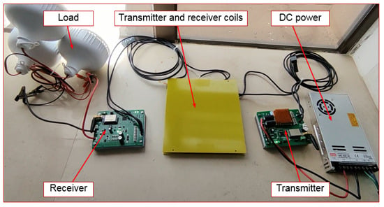
Figure 9.
A self-excited invert rectifier experimental equipment able to perform the SD and SS of the MOSFETs.
- (1)
- Experimental verification of the self-excited invert rectification method
Based on the aforementioned theory results, L2 and C2 comprise a series resonant tank, whose frequency determines that of the sine voltage at the Rx side. Furthermore, the switching frequency of Q5 and Q6 and the rectification frequency of the rectifier diode are determined by the frequency of the sine voltage stimulation on the Rx side. In Figure 10 and Figure 11, the working frequency of the self-excited invert rectifier is 75.7 kHz. Since the working frequency of the Tx is 75.7 kHz, the self-excited invert rectifier performs the FT. It can then be deduced that the self-excited invert rectifier can perform the SD and SS of the MOSFETs without a microcontroller, which greatly simplifies the structure of the invert rectifier.
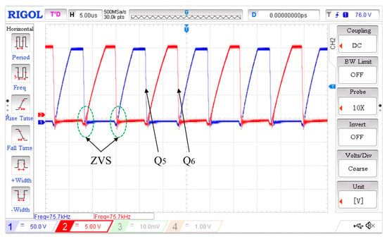
Figure 10.
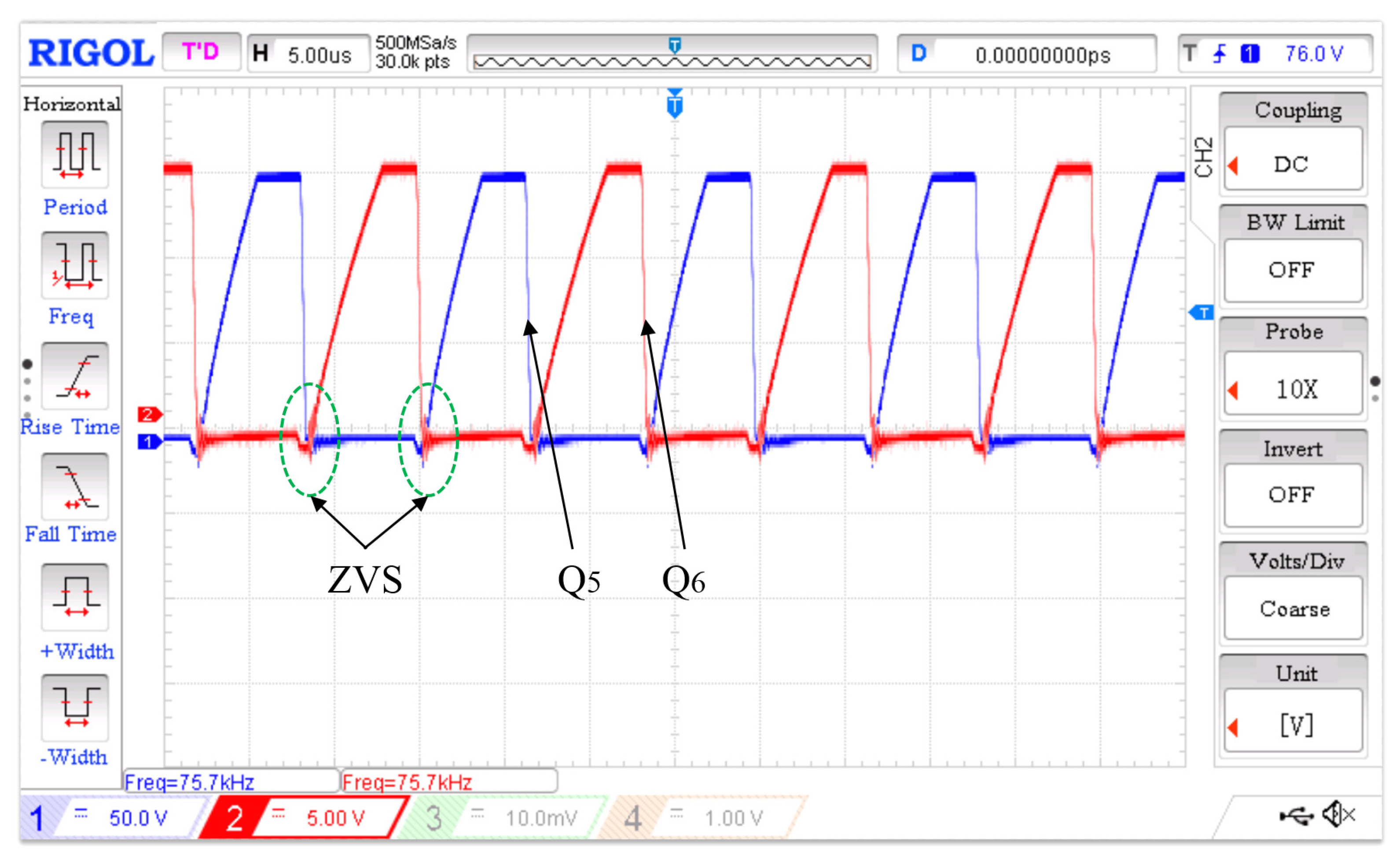
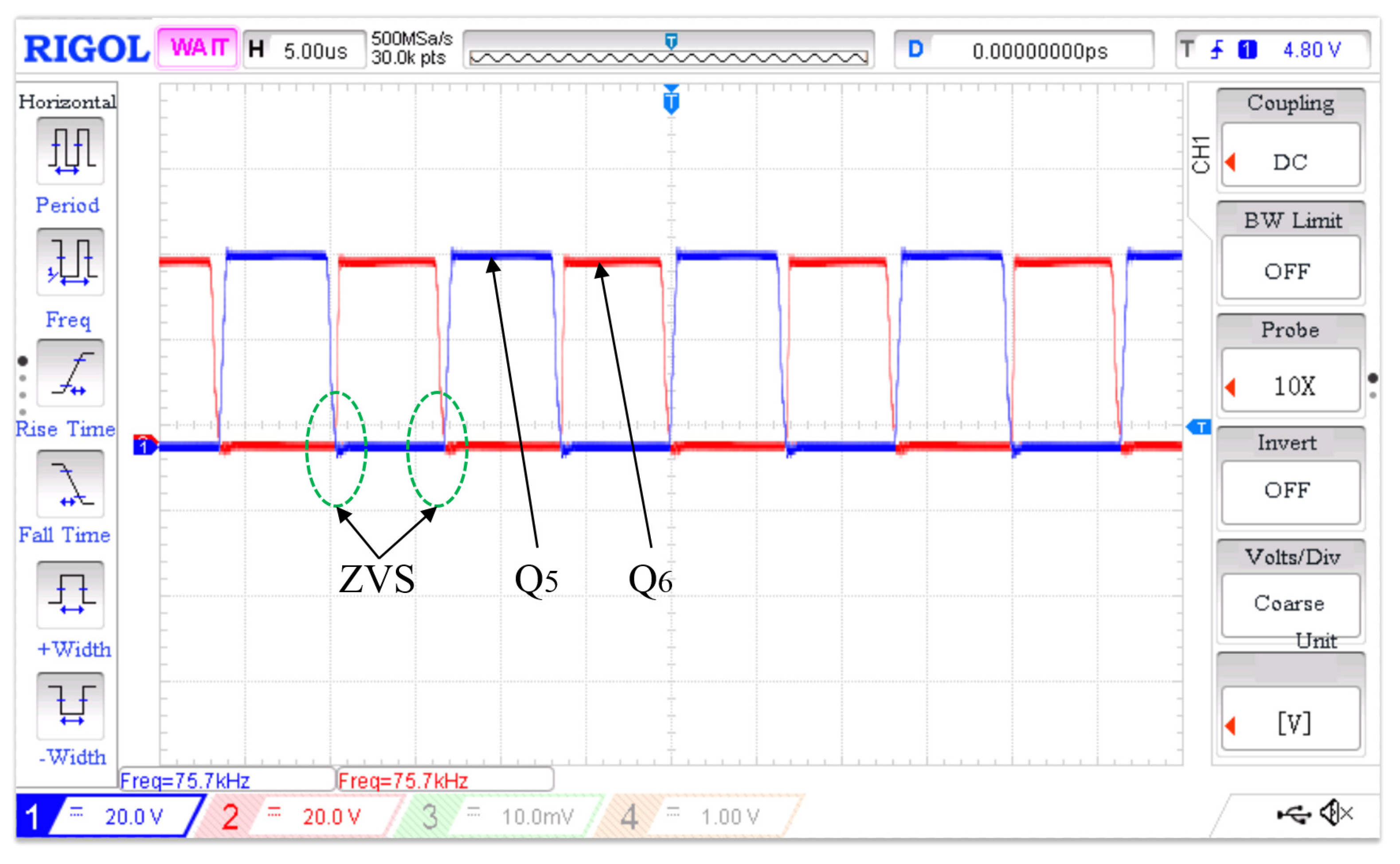
Gate drive waveform (gate−source voltage) of the Q5 and Q6 switching tubes.
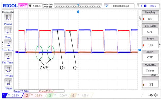
Figure 11.
Working waveform (drain−source voltage) of the Q5 and Q6 switching tubes.
In Figure 10, the time delay of the gate drive waveform between the Q5 and Q6 switching tubes is 220 ns. In Figure 11, the time delay of the working waveform between Q5 and Q6 is also 220 ns. This indicates that they are alternately turned on, which ensures the safe and reliable rectification of the self-excited invert rectifier. More precisely, the function of the zero-voltage switch (ZVS) is achieved in the self-excited invert rectifier using D1 and D2, R1 and R3, and R2 and R4. Thus, the invert rectifier circuit performs rapid and reliable switching between Q5 and Q6.
In summary, the experimental results are consistent with those of the theoretical analysis of Section 2. They show that the self-excited inverter rectification method is effective.
- (2)
- Experiment for reducing the power loss of the self-excited invert rectifier
According to the aforementioned theory results, R1–R4 resistors, Q5 and Q6, and D3 and D4 are affected by the power loss of the self-excited invert rectifier. This also affects the TE. Thus, key component parameters of the self-excited invert rectifier are required to increase the performance of the self-excited invert rectifier. The key component parameters are shown in Table 3.
Table 3.
Key component parameters of the self-excited invert rectifier.
R1 with R3 and R2 with R4 first construct two VDs to provide BVs for Q5 and Q6, respectively. R1 and R2 should have a suitable value, which allows us to obtain a suitable current to drive Q5 and Q6 (e.g., 1 kΩ in Table 3). Thus, high R1 and R2 values do not have sufficient current to drive Q5 and Q6 (e.g., 2 kΩ in Table 3). On the other hand, lower R1 and R2 values lead to circuit damage due to the excessive carried current (e.g., 560 Ω in Table 3).
In addition, R1 and D1 construct a circuit loop and quickly release power when Q6 is blocked. Note that R2 and D2 have the same function. The two circuit loops provide a quick energy release channel, which accelerates the mode switching and reduces the power loss of Q5 and Q6.
Moreover, a smaller drain-source on-state resistor of Q5 and Q6 results in a smaller power loss. In Table 3, the drain-source on-state resistor of APG011N04G is 0.9 mΩ, and its power loss is smaller than that of other components (e.g., AGM035N10A, BSC0702LS). However, the drain-source voltage should also be taken into consideration to be adapted to the WPT system. In this study, AGM035N10A was used to design the WPT experimental equipment.
Finally, a forward voltage of D3 and D4 results in a smaller power loss. In Table 3, the forward voltage of SB1060L is 550 mV, and its power loss is smaller than that of other components (e.g., FFSM0865B, SB10100L, and ST10100L). However, the forward voltage of FFSM0865B is 1.39 V, which is higher than that of other components. FFSM0865B was selected to design the WPT experimental equipment. When it functions, the temperature rapidly increases and the WPT experimental system is damaged. Additionally, the reverse voltage should also be taken into consideration in a WPT system. In this study, ST10100L was finally chosen due to its small forward voltage (590 mV) and higher reverse voltage (100 V).
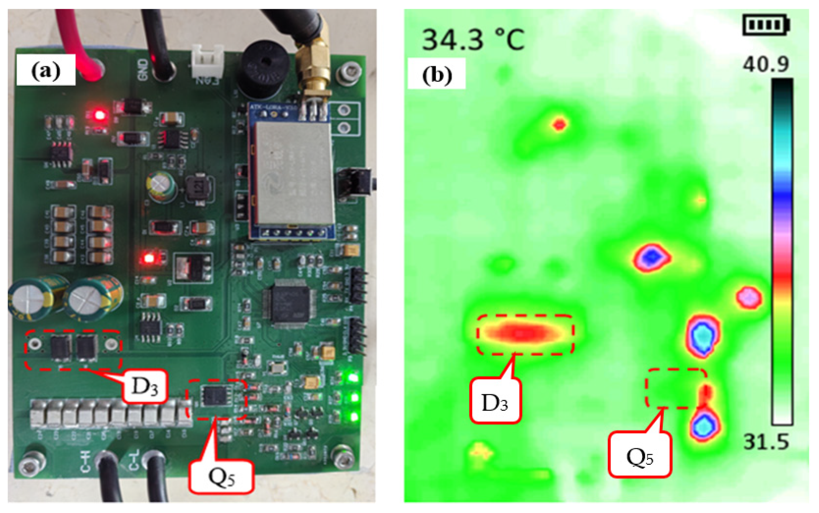
In Figure 12a, D3 and Q5 are on the front of the circuit board. However, D4 and Q6 are on the back. Because these two sets of components are symmetrically arranged on the front and back of the circuit board, they should have the same thermal image. Figure 12b shows the thermal image of the front of the circuit board. Several conducted measurements show that the temperatures of D3 and Q5 are lower than 34.3 °C. This indicates that the self-excited invert rectifier has higher performance when adopting the aforementioned key component parameters.
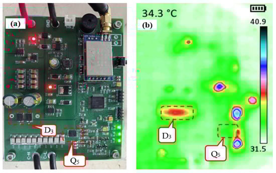
Figure 12.
(a) Circuit of the Rx and (b) temperature image of the self-excited invert rectifier.
In addition, the impact of temperature variation and load resistance needs to be considered in a WPT system. The power loss of the self-excited invert rectifier is low when the system works at an industrial-grade temperature. Moreover, appropriate load resistance is beneficial for improving TE.
In summary, the experimental results for reducing the power loss are consistent with the theoretical analysis of Section 3. It shows that the measures for reducing the power loss of the self-excited invert rectifier are effective.
- (3)
- Experiment for increasing the TE of the self-excited invert rectifier
According to the aforementioned optimizing results of the key component parameters, in Figure 13 and Figure 14, the OP P1 and TE η1 are obtained using the full-bridge inverter rectifier of the Rx. On the other hand, the OP P2 and TE η2 are obtained using the self-excited invert rectifier of the Rx. Due to the selection of suitable key component parameters for the self-excited invert rectifier, the OP of the WPT system with the self-excited invert rectifier is improved by more than 10 W. Similarly, the TE with the self-excited invert rectifier is increased by more than 5%. More precisely, it reaches 86.2%, while it is only 91.4% in the case of only optimizing the Rx side.
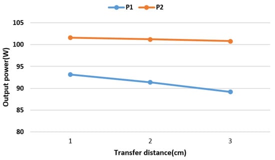
Figure 13.
OP of the system as a function of the distance.
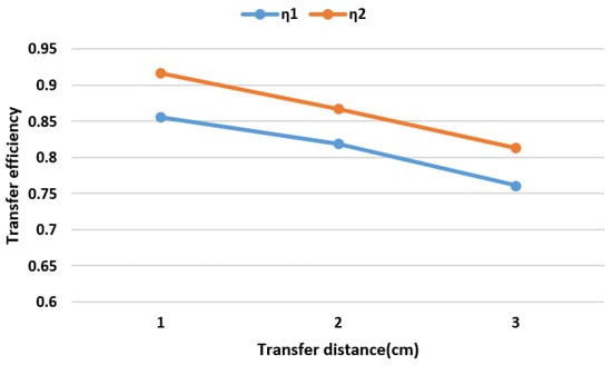
Figure 14.
TE of the system as a function of the distance.
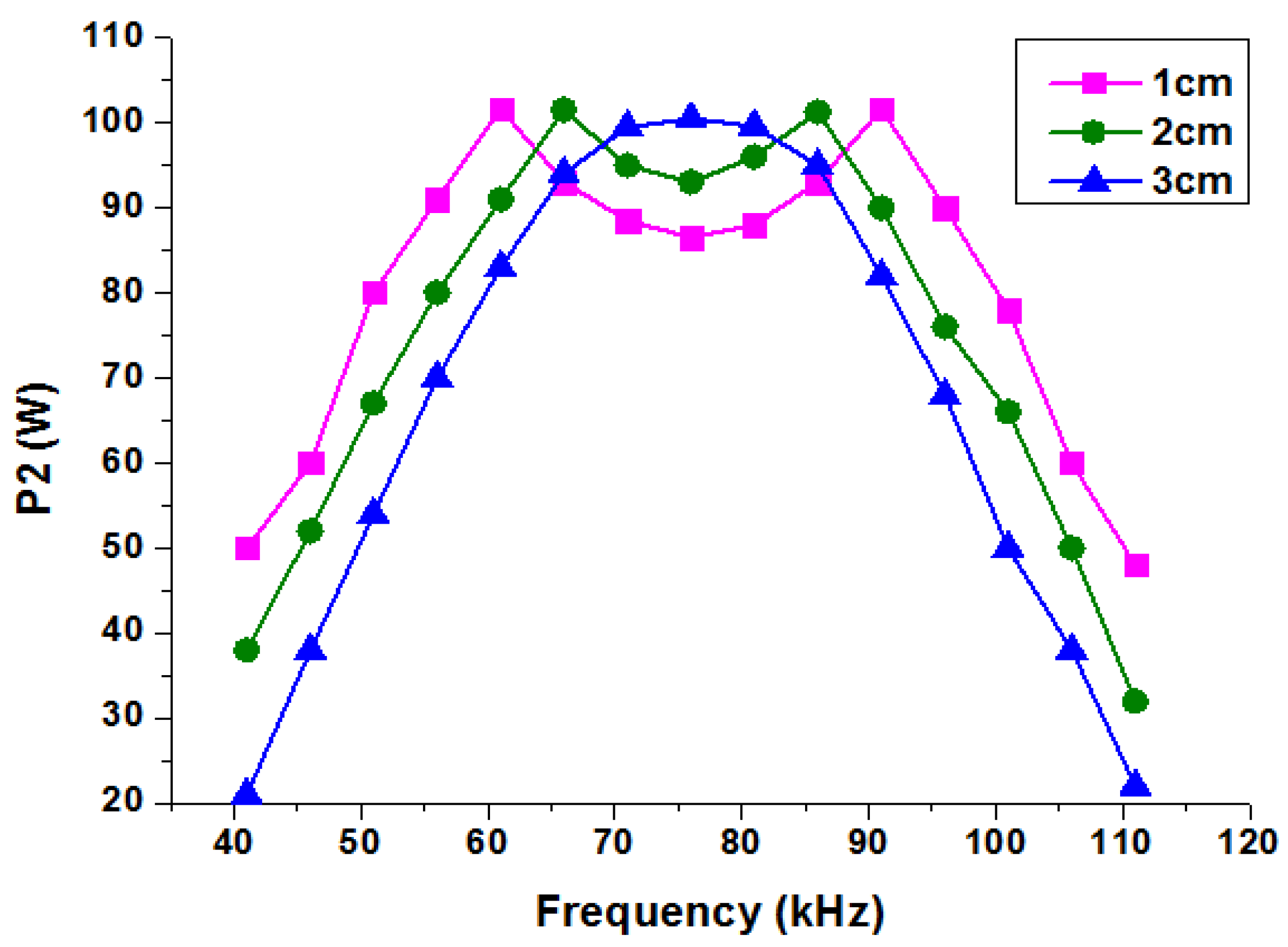
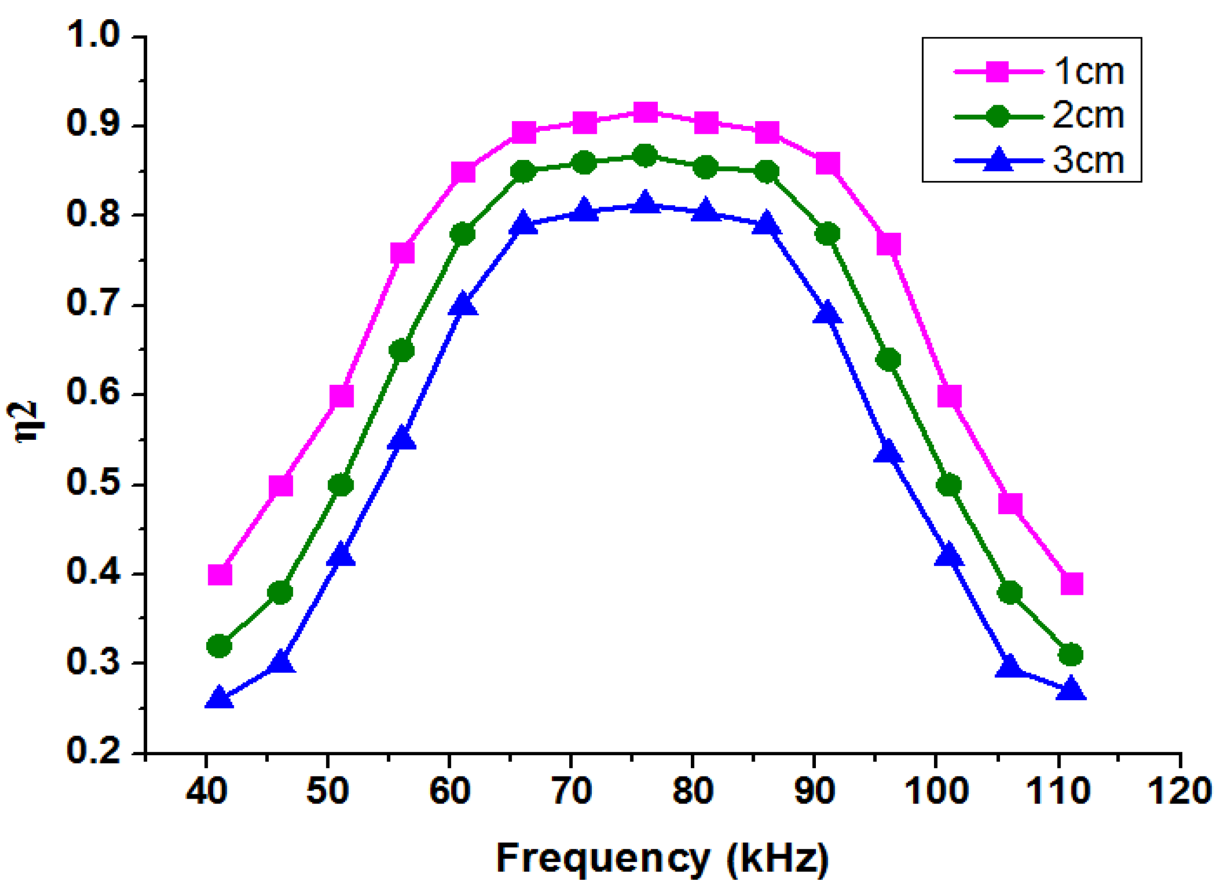
According to the aforementioned results of the key component parameters, the OP P2 and TE η2 are obtained at different frequencies, which are shown in Figure 15 and Figure 16. It can be seen that, for a transfer distance of 3 cm, the high and flat OP P2 peaks are reached around 75.7 kHz. For a transfer distance of 1 cm, the peaks of the OP P2 occur at 61 kHz and 91 kHz, respectively. Additionally, for a transfer distance of 2 cm, the peaks of the OP P2 occur at 66 kHz and 86 kHz, respectively. Thus, the frequency splitting of the OP occurs at transfer distances of 1 cm and 2 cm [3,21]. However, the high and flat TE η2 peaks are reached at around 75.7 kHz. The value of the TE η2 is increased as the transfer distance decreases. According to the aforementioned analysis results, it can be concluded that the optimization of TE is needed to consider the impact of frequency splitting. Thus, in the self-excited invert rectifier experimental equipment, the working frequency of the Tx side is adaptively changed to obtain the maximum value of the TE when the transfer distance changes.
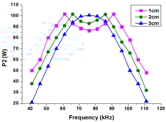
Figure 15.
OP P2 of the system as a function of the frequency.
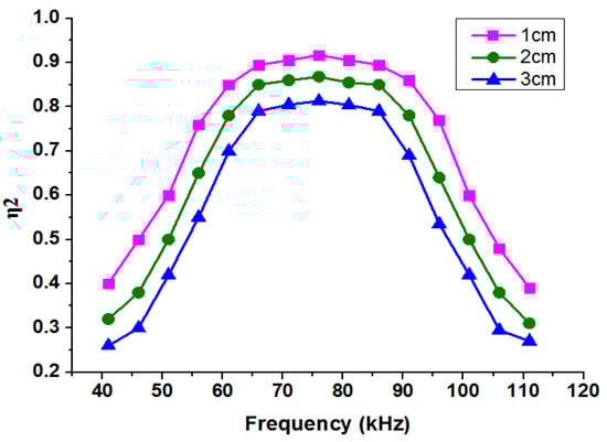
Figure 16.
TE η2 of the system as a function of the frequency.
In summary, the experimental results are consistent with those of the theoretical analysis. They show that the self-excited inverter rectification method is effective. In addition, the self-excited invert rectifier can perform the SD and SS of the MOSFETs as well as the FT function without a microcontroller. This method provides a practical solution for reducing the complexity of the rectifier. It can be clearly seen that the TE is increased using the self-excited invert rectifier and the optimized key component parameters.
5. Conclusions
In this paper, a novel self-excited invert rectification method was proposed to design the invert rectifier of the Rx. This self-excited invert rectifier can perform the SD and SS of the MOSFETs as well as the FT function without a microcontroller. In addition, the TE of the WPT system with the self-excited invert rectifier and optimized key component parameters is increased by more than 5%. Finally, the self-excited invert rectifier of the Rx provides a practical solution for reducing the complexity of the WPT system.
Author Contributions
S.L.: conceptualization, methodology, software, validation, writing—original draft preparation. X.Y.: data curation. G.W.: writing—review and editing. Y.L.: writing—review and editing. All authors have read and agreed to the published version of the manuscript.
Funding
The work was supported by the Guangxi Natural Science Foundation (Grant Nos. 2022GXNSFAA035590 and 2021GXNSFBA196051) and the High Level Talent Foundation Project of Guilin University of Electronic Technology (UF20008Y).
Data Availability Statement
The original contributions presented in this study are included in the article. Further inquiries can be directed to the corresponding author.
Conflicts of Interest
The authors declare no conflicts of interest. The founding sponsors had no role in the design of the study or in the decision to publish the results.
References
- Tesla, N. Electrical Energy. U.S. Patent 1,119,732, 1 December 1914. [Google Scholar]
- Kurs, A.; Karalis, A.; Moffatt, R.; Joannopoulos, J.D.; Fisher, P.; Soljacic, M. Wireless Power Transfer via Strongly Coupled Magnetic Resonances. Science 2007, 317, 83–86. [Google Scholar] [CrossRef]
- Sample, A.P.; Meyer, D.T.; Smith, J.R. Analysis, Experimental Results, and Range Adaptation of Magnetically Coupled Resonators for Wireless Power Transfer. IEEE Trans. Ind. Electron. 2011, 58, 544–554. [Google Scholar] [CrossRef]
- Qin, R.; Li, J.; Sun, J.; Costinett, D. Shielding Design for High-Frequency Wireless Power Transfer System for EV Charging With Self-Resonant Coils. IEEE Trans. Power Electron. 2023, 38, 7900–7909. [Google Scholar] [CrossRef]
- Liu, S.; Yan, X.; Xu, G.; Wang, G.; Liu, Y. An Eight-Coil Wireless Power Transfer Method for Improving the Coupling Tolerance Based on Uniform Magnetic Field. Processes 2024, 12, 2109. [Google Scholar] [CrossRef]
- Liu, S.; Liu, Y. Transfer characteristics of the MCR-WPT system using two series transmitting coils. Circuit World 2019, 46, 48–54. [Google Scholar] [CrossRef]
- Tang, J.; Na, T.; Zhang, Q. A Novel Full-Bridge Step Density Modulation for Wireless Power Transfer Systems. IEEE Trans. Power Electron. 2023, 38, 41–45. [Google Scholar] [CrossRef]
- Yang, Y. A Passive Augmented Circuit for EMI Reductions of Full-Bridge Inverters With Conventional Phase Shift Control in Wireless Power Transfer Systems. IEEE Trans. Power Electron. 2023, 38, 13286–13297. [Google Scholar] [CrossRef]
- Kavimandan, U.D.; Galigekere, V.P.; Ozpineci, B.; Onar, O.; Mahajan, S.M. The Impact of Inverter Dead-Time in Single-Phase Wireless Power Transfer Systems. IEEE Trans. Power Electron. 2022, 37, 1074–1089. [Google Scholar] [CrossRef]
- Xiong, W.; Yu, Q.; Liu, Z.; Zhu, Q.; Su, M.; Zhao, L.; Hu, A.P. A Dual-Frequency-Detuning Method for Improving the Coupling Tolerance of Wireless Power Transfer. IEEE Trans. Power Electron. 2023, 38, 6923–6928. [Google Scholar] [CrossRef]
- Li, K.; Tan, S.-C.; Hui, R. Dynamic Response and Stability Margin Improvement of Wireless Power Receiver Systems via Right-Half-Plane Zero Elimination. IEEE Trans. Power Electron. 2021, 36, 11196–11207. [Google Scholar] [CrossRef]
- Liu, J.; Xu, F.; Sun, C.; Loo, K.H. A Soft-Switched Power-Factor-Corrected Single-Phase Bidirectional AC–DC Wireless Power Transfer Converter with an Integrated Power Stage. IEEE Trans. Power Electron. 2022, 37, 10029–10044. [Google Scholar] [CrossRef]
- Liu, X.; Wang, Y.; Chen, H.; Mai, J.; Xu, D. A Bidirectional WPT System Using Double-sided LCC Compensation Topology and Full-bridge Active Rectifier. In Proceedings of the 2022 IEEE Transportation Electrification Conference and Expo, Asia-Pacific (ITEC Asia-Pacific), Haining, China, 28–31 October 2022; pp. 1–7. [Google Scholar]
- Wu, X.; Yan, H.; Xiao, J.; Chen, S.; Wu, N.; Mo, Y. Analysis of Phase-Shifting Constant Voltage Control of LCC-S Wireless Power Transfer System. In Proceedings of the 2023 International Conference on Electronics and Devices, Computational Science (ICEDCS), Marseille, France, 22–24 September 2023; pp. 54–58. [Google Scholar]
- Wu, W.; Luo, D.; Hong, J.; Tang, Z.; Chen, W. A Six-Switch Mode Decoupled Wireless Power Transfer System with Dynamic Parameter Self-Adaption. Electronics 2023, 12, 2314. [Google Scholar] [CrossRef]
- Wang, Y.; Liu, W.; Huangfu, Y. A Wireless Power Transfer System with Robust Primary-Sided Current Based on the Self-Excited Inverter. In Proceedings of the 2019 IEEE International Conference on Industrial Technology (ICIT), Melbourne, VIC, Australia, 13–15 February 2019. [Google Scholar]
- Yao, W.; Weiguo, L.; Yigeng, H.; Yuntian, L. Wireless Power Transfer System Based on the Self-Excited Inverter. Trans. China Electrotech. Soc. 2019, 34, 4751–4760. [Google Scholar]
- Zhao, Z.; Luo, B.; Tan, T.; Wang, C.; Sun, Z. Improved Self-Excited Resonant Wireless Power Transmission System. J. Shanghai Jiao Tong Univ. 2023, 57, 859–867. [Google Scholar]
- Yang, J.; Chen, W.; Xie, W. Research on Wireless Power Transmission System Based on Self-excited Push-pull Oscillator. J. Power Supply 2021, 19, 142–152. [Google Scholar]
- Zhang, X.; Yuan, Z.; Yan, Q.; Wei, B.; Wang, S. Analysis of the Magnetic Shielding Characteristics of Magnetic Coupling Resonant Wireless Power Transmission System Based on Self-excited Push-pull Converter. Proc. CSEE 2018, 38, 555–561+686. [Google Scholar]
- Liu, S.; Tan, J.; Wen, X. Research on the Impedance Characteristic of a Two-Coil Wireless Power Transfer System. IEICE Trans. Electron. 2018, 101, 711–717. [Google Scholar] [CrossRef]


Disclaimer/Publisher’s Note: The statements, opinions and data contained in all publications are solely those of the individual author(s) and contributor(s) and not of MDPI and/or the editor(s). MDPI and/or the editor(s) disclaim responsibility for any injury to people or property resulting from any ideas, methods, instructions or products referred to in the content. |
© 2025 by the authors. Licensee MDPI, Basel, Switzerland. This article is an open access article distributed under the terms and conditions of the Creative Commons Attribution (CC BY) license (https://creativecommons.org/licenses/by/4.0/).