1. Introduction
With the gradual development of electronic devices to a modular, high-performance and multi-functional state, their packaging technology also shows a trend of being high-density [
1]. During the operational phase, circuit boards are frequently subjected to environmental stresses such as mechanical stress (vibration, impact, etc.) [
2], thermal stress (high temperature, low temperature, temperature fluctuations, etc.) [
3], electrical stress (over-voltage, over-current, etc.), and chemical corrosion (humidity, salt spray, etc.), which can lead to the failure of the circuit board. Additionally, improper processing and material defects [
4] can also contribute to the malfunctioning of circuit boards.
Vibration as a complex load has been the subject of research for a long time [
5]. Therefore, it is very important to understand the failure mechanism of components under vibration conditions. Printed Circuit Boards (PCBs) are important components of electronic equipment, and their sensitivity to vibration directly affects the reliability and environmental adaptability of electronic equipment [
6].
On a PCB, the solder joint is a key part of signal transmission, mechanical connection and electrical conduction, so solder joint failure is closely related to PCB failure. In order to strengthen the reliability of solder joints, some scholars chose to optimize the solder. Yomamoto et al. [
7] investigated the effects of Ni addition on the microstructure, tensile, and fatigue properties of Sn-6.4Sb-3.9Ag (mass%). Li et al. [
8] prepared SN-25SB-X Ag (x = 0, 2.5, 3.0, and 3.5, where x is the mass percentage) solder alloys by adding Ag to Sn-25Sb solder. The mechanical properties of the solder joints were improved.
The above research only improved the mechanical properties of solder joints by optimizing the solder. In order to improve the vibration reliability of the whole PCB, it is necessary to design and optimize the key components, solder joint distribution, and substrate structure. Some scholars employed scanning imaging techniques to detect defects in circuit boards. For instance, Wang et al. [
9] proposed laser-induced ultrasound scanning imaging, which offers the advantage of high-resolution imaging for small-diameter defects when compared to traditional infrared thermography. With this technology, faults can be detected at an early stage, so repairing the fault area before mass production can prevent damage to the entire board. Some scholars conducted vibration analysis of PCBs through finite element analysis to study its dynamic response characteristics after vibration excitation, or to predict its fatigue life under random vibration load, which can provide a basis for the optimization of PCB design. Muhammad et al. [
2] estimated the remaining useful life (RUL) of electronic modules by means of vibration testing and finite element analysis techniques. Karthiheyan et al. [
10] used JEDEC standards for an experimental verification of their results, verified the finite element design used for their study, and conducted random vibration experiments through finite element analysis. The fatigue life of PCB under different random vibration environments was predicted and compared.
To sum up, finite element analysis plays an important role in vibration reliability analysis [
11,
12,
13,
14,
15], but the following problems need to be solved in practical applications: (1) A lack of qualitative and quantitative analysis of fault sample data in specific industries, resulting in an oversimplification of finite element models. (2) The failure mechanisms of actual engineering machinery control systems have not been deeply studied. Aging tests require a long time and high cost, and it is difficult to locate weak links accurately.
In this paper, by comparing the results of the effects and criticality analysis (FMECA), modal experiment, and modal simulation, a finite element model of a rig control circuit board is established. Then, the finite element model is analyzed by random vibration simulation, and its weak links under random vibration loads are obtained, which provide an optimization basis for a vibration reduction design of the PCB. Finally, based on the analysis results, optimization suggestions are put forward. The main novelties and contributions of this study are summarized as follows:
Through the mutual verification and comparison of the modal experiment, modal simulation, and FMECA, the finite element model is closer to reality.
The vibration reliability of the rig control circuit board under actual working conditions is analyzed in depth and feasible optimization suggestions are put forward. It is expected to provide fast, accurate, and efficient technical support for the reliability improvement of similar mechanical and electrical products at the use stage.
The rest of this paper is organized as follows:
Section 2 introduces the basic theories of FMCEA, FTA, and modal analysis.
Section 3 introduces the establishment of the finite element model. In
Section 4, the analysis results of the modal and random vibration simulations are given and the optimization suggestions for the rig control circuit board are put forward.
Section 5 summarizes the full paper.
4. Modal Analysis and Random Vibration Analysis
4.1. Modal Calculation
In this paper, the structural characteristics of the system were obtained via modal analysis, and its natural frequency and mode were obtained. The modal optimization was realized by changing the natural frequency of the product. The default Block Lanczos method of ANSYS was used to analyze the mode of the PCB with constraints, which provided accurate modal solutions for the following random vibration analysis and optimization. The frequency range of this analysis was set to be 0~1000 Hz, and the first four mode shapes were analyzed. According to the actual constraints, fixed constraints were added to the four positions A, B, C, and D in
Figure 4. The first four mode shapes are shown in
Figure 5, and the first four vibration frequencies are shown in
Table 6.
According to the mode shape diagram, the first two orders of mode shapes are dominated by single bending deformation. As the order increases, the combined deformation of bending and torsion begins to appear. Under different order modes, it can be seen that the maximum deformation occurs at different locations, which indicates that there are multiple structural weaknesses in the substrate and important components. In the first mode response, the substrate was in a center-symmetric bending state, and the capacitor near the midline is most affected and prone to failure. The maximum amplitude (marked Max in
Figure 5) is near the pin and solder joint. In the high-order modal response, the four corners of the substrate gradually warped, and the maximum stress was more concentrated on each side of the substrate. Since the maximum stress point is close to the chip inductor and chip component, this can lead to chip inductor and chip failure. In the reliability optimization of the PCB, the performance and position of the core components that are susceptible to interference should be considered, such as diodes, chip inductors, and chips, as well as the welding quality of the solder joints. The following methods can avoid the occurrence of mechanical resonance when the PCB is working.
Method 1: The staggered degree between the natural vibration frequency and vibration source frequency is greater than 20%, which can avoid resonance [
25]. The equation for calculating the staggered degree of each mode frequency is as follows:
In order to avoid a Stagger degree of less than 20%, the frequency isolation device can be used to reduce the influence of the PCB by the external excitation frequency.
Method 2: Change the method of fixing the supports, or increase the number of fixed supports to improve the natural frequency of the PCB and avoid mechanical resonance.
4.2. Modal Test
There are multiple sources of errors in the simulation process, including model error, material attribute error, mesh density error, etc. [
26]. If there is a big difference between the modal test results and the simulation results, the simplified model needs to be modified to ensure the reliability and accuracy of the simulation results. The natural frequency of the modal test object is high in this paper, so the influence of gravity can be ignored.
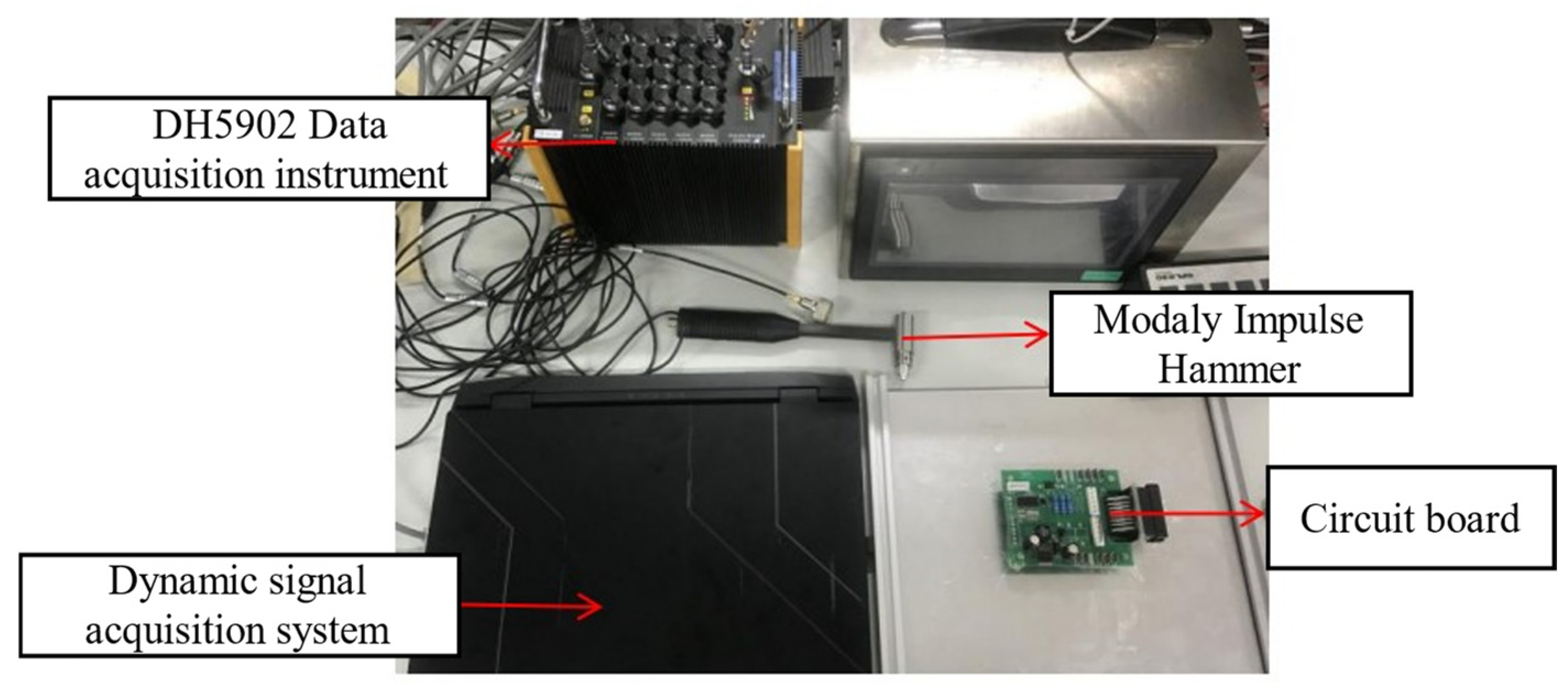
The modal test equipment included a DHDAS dynamic signal acquisition and analysis system, force hammer, ICP-type acceleration sensor, and DH5902N data acquisition instrument. The test method was a single-point vibration pickup force measurement. Firstly, a force hammer was used to strike the excitation points near the measuring points to generate pulse excitation, and the response of the excitation points was measured by the acceleration sensors. After the frequency response function between the force measurement point and the response point was obtained, the modal frequency and modal mode of the experimental object were analyzed and calculated. The experimental data obtained through the MAC modal test were compared with the simulation data to verify the accuracy of simulation modeling. The test equipment is shown in
Figure 6.
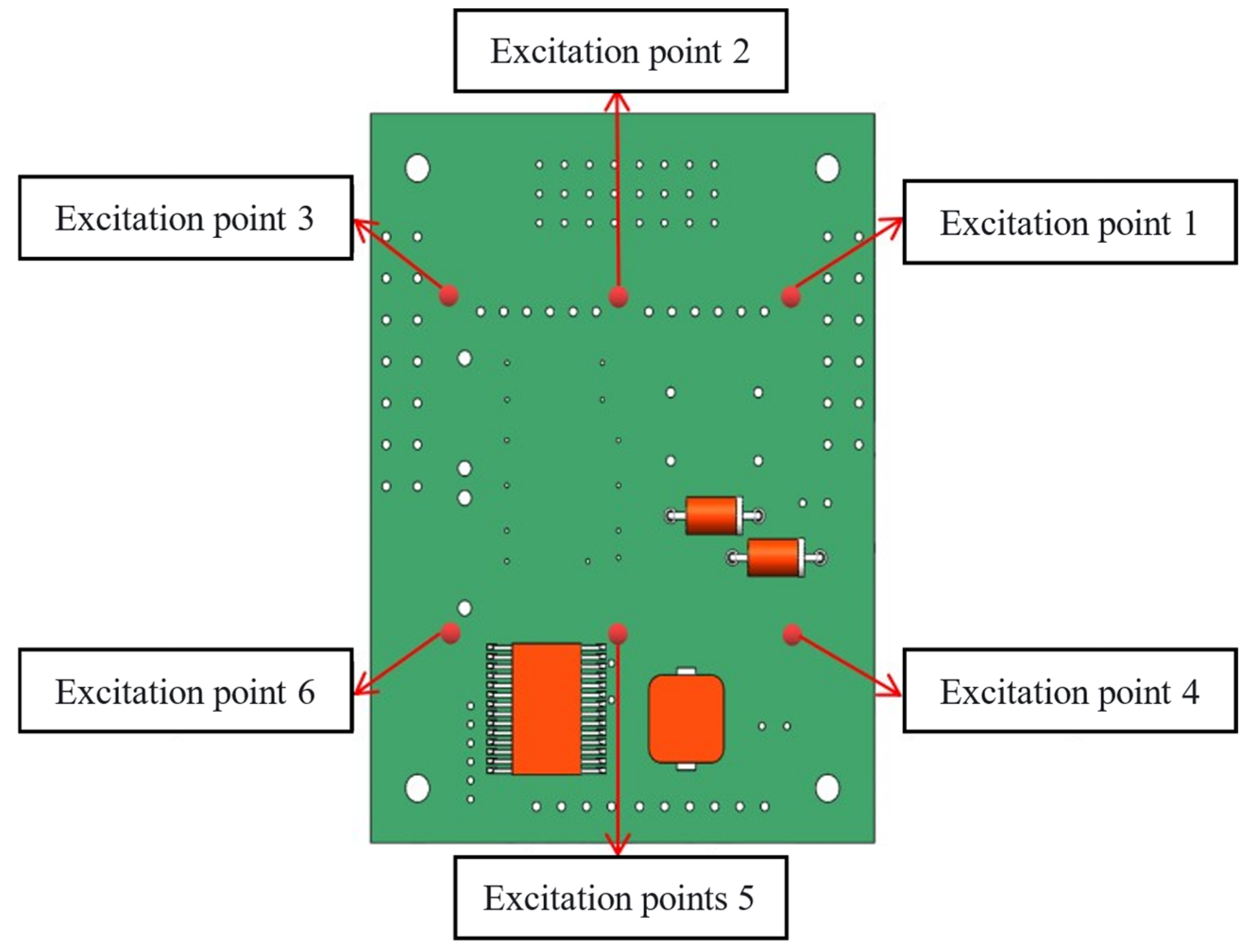
The force hammer and the acceleration sensor were connected to the data acquisition instrument, and the storage mode and basic parameters of the signal were set. The analysis bandwidth was set to 391 Hz; each excitation point was tapped five times to take the average value; and the trigger level of the force hammer channel was set to 10%. After each trigger, you can choose whether to retain it or not to avoid a change in the average times of the counter caused by slight miscontact. The positive direction of the sensor and the force hammer was the Z direction (vertical upward). Because the substrate deformation of the low-order mode was symmetrical at the middle line, the excitation points were set above and below the middle line, close to the position where the vibration was more obvious. The arrangement of the excitation points is shown in
Figure 7. The modal test results are shown in
Table 7.
It can be seen from
Table 3 that the error between the results of the modal test and modal simulation is within 5%, so it can be verified that the reliability of the results of the modal simulation is high. The PCB is likely to be damaged by mechanical resonance when the natural frequency is close to the working excitation frequency in a low-order-mode operating environment. In order to further obtain the weak part of the PCB under the actual working conditions, it was necessary to conduct a random vibration simulation analysis of the model.
4.3. Random Vibration Analysis
The failure of electronic equipment is mostly due to the vibration fatigue caused by broadband random vibrations. With damage caused to the components or solder joints of the equipment, the stability and reliability of the PCB will be affected. Researchers have proposed many optimization schemes in PCB structure distribution, solder joint quality reliability, and constraint arrangement, but most of them are based on simulation analysis results [
27,
28,
29]. In this paper, combined with the qualitative analysis results of FMECA, random vibration simulation analysis and modal analysis were used to verify weak parts, which provides a theoretical basis for reliability optimization design.
Using the frequency response function and modal superposition technique, the absolute value of the mean square response of the
i-order free displacement under a weakly damped condition can be obtained as [
30,
31]:
where
is the dynamic range of the self-spectral density function,
is the quasi-static part of the self-spectral density function, and
is the cross-spectral density function of the static and dynamic degrees of freedom.
represents the real part of the entry.
Through random vibration analysis, the corresponding displacement solution and stress solution under a certain power spectral density can be obtained. These solutions can be expressed as probability solutions under the category of statistics, which can be divided into 1σ, 2σ and 3σ.
The module of random vibration in ANSYS was used to simulate the random vibration of the PCB, and its constraint was consistent with the modal analysis. The frequency range of the acceleration power spectral density was set from 1 to 350 Hz, and the excitation direction was perpendicular to the surface of the substrate. In this paper, the first mode frequency and 1σ were used for calculation. The equation is as follows:
where
γ is the first-order mode participation coefficient, and
is the 1σ unilateral upward displacement response.
φ is the maximum mode amplitude of the first-order mode shapes.
M represents the generalized mass, PSD represents the power spectral density, and
f represents the first-order natural frequency.
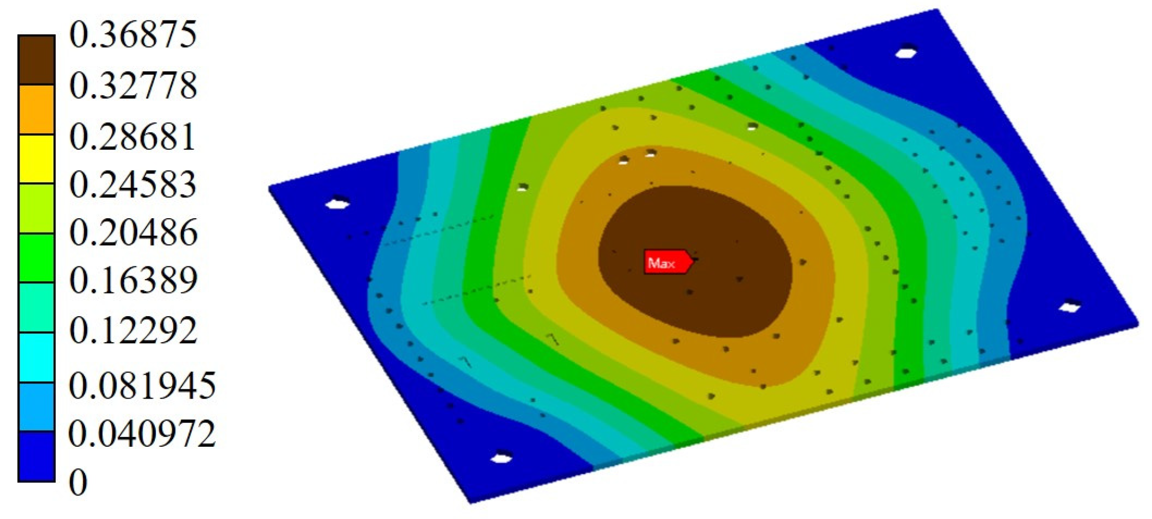
It can be seen from
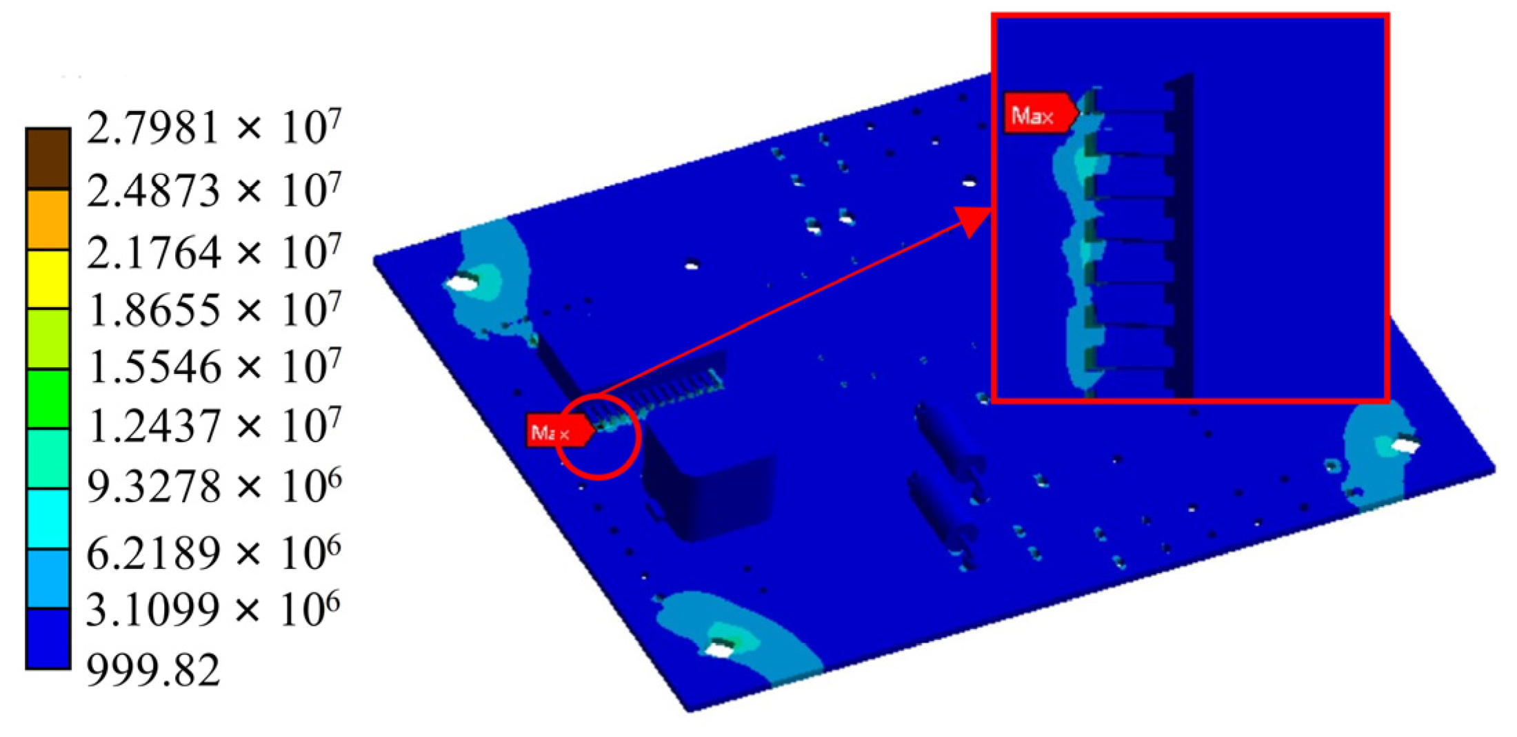
Figure 8 that the response value of the PCB in the first-order mode y direction is 0.36875 mm. The theoretical response value obtained by referring to Equation (15) is 0.313 mm, and the two results are close. Furthermore,
Figure 9 shows that at the 1σ solution, the stress is minimal near the center line of the circuit board, and the stress is concentrated near the rigid support points, pins, and through-holes. The maximum stress was found at the second pin solder joint of the main control chip, reaching 2.79 × 10
7 Pa, and the probability of a 1σ solution was 68.269%. In summary, the random vibration simulation process is reasonable and reliable.
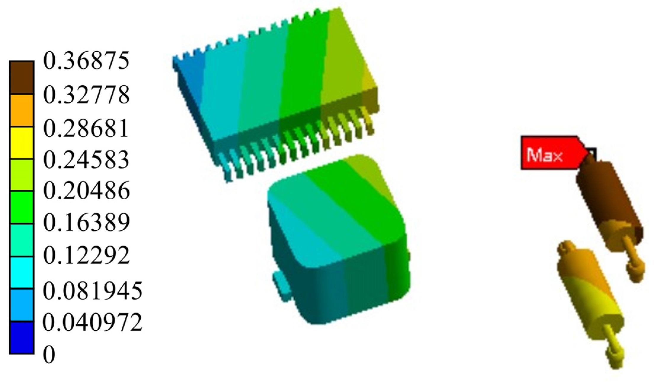
As can be seen from the component vibration response in
Figure 10, the maximum vibration response of the diode is located at the joint of the welding ball and the pad. In the actual work process, it is easy for this to be affected by external vibration excitations, resulting in the fatigue damage of materials and structures gradually increasing until failure. The displacement at the center line of the substrate is the largest, and the deformation decreases to both sides, which is consistent with the first-order modal response results obtained from the modal analysis. The capacitive electronic components near the center line are most affected by vibration, so they need to be optimized for solder joints or pins. In addition, materials with higher natural frequencies should also be given priority for the substrate.
4.4. Optimization
In summary, the structural design optimization methods of a drilling rig PCB based on random vibration simulation dynamic analysis are as follows:
- 1.
Reliability optimization in packaging.
Increase the PCB with a fastening point between components to increase the resistance of the solder joint performance of vibration;
An EC-2216 epoxy adhesive is used to reinforce the device body, which can disperse most of the stress generated by random vibrations of the PCB;
In the actual processing, the height and diameter of the chip welding post can be appropriately increased within the allowable range of process conditions to improve the vibration fatigue reliability of the structure;
The vibration stress response between the pins, solder joints, and pads can be reduced by reasonably controlling the side-length shape parameters.
- 2.
Reliability optimization of the substrate.
As the key substructure of the PCB, the substrate should have high reliability. The use of a high-frequency plate instead of a low-frequency plate can improve the performance parameters of the material, increasing the low-order-mode frequency. In this way, the occurrence of mechanical vibration fatigue damage can be reduced.
After replacing the low-frequency plate with the FR-4 high-frequency plate, the modal analysis was re-performed. The frequencies of each mode obtained are shown in
Table 8. The low mode order of the optimized PCB is much higher than the excitation frequency in the working state, and the resonance phenomenon can be avoided well. In addition, adding an anti-vibration seat or reinforcing bar can also reduce the response of PCB caused by vibration load [
32,
33].


