Article

Highly Polarized SERS Based on Random Working Domains Composed of Nanorod Arrays for Self-Referenced Detection

1
School of Material and Environmental Engineering, Hangzhou Dianzi University, Hangzhou 310018, China
2
Zhejiang Laboratory, Hangzhou 311100, China
3
Department of Physics, Xiamen University, Xiamen 361005, China
*
Author to whom correspondence should be addressed.
Chemosensors 2023, 11(8), 462; https://doi.org/10.3390/chemosensors11080462
Submission received: 8 June 2023 / Revised: 1 August 2023 / Accepted: 14 August 2023 / Published: 16 August 2023
(This article belongs to the Special Issue SERS Sensing Technology: Research, Progress and Applications)

Abstract

:
When Ag film is sputtered onto polystyrene (PS) spheres, the curved Ag nanocaps form with scattered Ag nanoparticles along the brim of the Ag nanocap. Ion etching results in parallel PS nanorods due to the masking effects of the scattered Ag nanoparticles when the Ag cap array is transferred to another substrate with the top down. The highly polarized SERS substrate of random working domains composed of parallel nanorods is prepared when another 5 nm film is deposited. The nanorod diameters range from 10 nm to 20 nm, depending on the sizes of the masking Ag nanoparticles prepared by the magnetron control system and the ion etching process. Compared with other techniques, our nanorods have the advantages of highly ordered patterns in each domain, which show the excellent behavior of the polarized SERS for all PS spheres. This polarized SERS substrate is used to detect thiram with a concentration as low as 10−9 M when the background noise is successfully removed by a self-reference technique.
Keywords:
LSPR; ion etch; nanorod

1. Introduction

When a laser is chosen as the excitation source, Raman spectra have wide applications because molecule structures can be deduced from the characteristic peaks. This means that for a sample with a very low concentration or molecules with a small scattering cross section, there are still significant challenges for modern detection due to the weak Raman signals. In addition to the enrichment method, a method that can enhance the Raman signals without complex treatment is also a good choice for practical applications. Local surface plasmon resonance (LSPR) happens when the wavelength of incident light is in resonance with the LSPR band of the metal nanostructure, which leads to a strong local field on the metal nanostructure surface [1,2,3,4]. When some molecules are near or linked to the metal nanostructure surface, the Raman signals show great enhancement, which is called surface-enhanced Raman scattering, or SERS. Theoretical and experimental studies show SERS with single-molecule identification, which is suitable for chemical sensing with ultrahigh sensitivity. In the investigations of the working mechanism for SERS, the observed enhancements of the strong local field have been clearly contributed to by physical enhancement due to the local electromagnetic coupling and chemical enhancement due to the charge transfer process [5,6,7]. The LSPR characteristics of metal nanostructures depend on several factors, such as the shape and size of the nanostructures, the chemical component of the materials, the distance between nanostructures, and the direction of polarization of the incident light [8,9,10]. With the efforts of many researchers, LSPR effects have been found to have applications in several interesting fields, such as surface enhanced Raman scattering (SERS), plasmon mediated chemical reactions (PMCRs), metamaterials, and so on [11,12,13,14]. Nowadays, researchers focus on the main challenges for SERS development: realizing SERS with ultrahigh sensitivity and getting stable SERS signals. These concerns include the uniformity of nanostructures [9], consistency of SERS signal [10], and influences of the background noises [11]. To improve the uniformity and consistency of SERS signals, nanostructures with high symmetry are prepared, such as sphere-like nanoparticles, honeycomb-like nanostructures, and ring-like nanogaps. Shift-excited Raman differential spectroscopy (SERDS) and modulated Raman spectroscopy are also chosen to improve the signals, but the process of changing the excitation source in the Raman setting is complex and troublesome [15,16,17,18]. Recent research shows the SERS intensity changes with the incident light when the polarized SERS signals are measured with the angular dependence for some ordered nanostructure arrays, while the polarization-independent interference signals show no changes yet; for example, the background noises. Therefore, the background signals can be eliminated by the subtraction of Raman intensity in different polarization directions, which is preferred for the super-resolution spectral analysis techniques of anisotropic nanostructures [19,20,21,22,23,24,25]. According to previous studies, polarization dependence is related to the shape of nanostructures; anisotropic nanostructures usually have polarization dependence [26,27,28], as do nanowires [24], nanorods [25], nanocubes [27], and nanoparticle aggregates [29]. When the incident light irradiates these structures, the strongest polarization intensity is observed in the long axis direction of the structure [27]. A theoretical simulation shows the polarization dependence on the structural parameters of the nanostructures, such as the chemical composition, the nanostructure size, the nanostructure shape, and the direction of incident light [16,17,18,19,20]. Zhu et al. investigated the polarization dependence of SERS in the hexagonal, close-packed nanoperiodic Ag nanoparticle arrays, which show angle-dependent coupling because the patterned nanostructures give anisotropic coupling [28]. Gao et al. investigated the polarization dependence of hexagonal, tightly packed, tilted silver nanoroded arrays with good uniformity and reproducibility, obtaining the fundamental cause of SERS polarization dependence by quantitative 3D numerical simulations of the distribution of adjacent nanoroded hotspots. Polarization dependence is deeply affected by the uniformity of nanostructures [29]. Some nanostructures can only measure the polarization dependence between single or several nanostructures because of the uncontrollability of the direction of nanostructures. Chen et al. studied the polarization dependence of the crossed nanowires and proved that it is independent of the diameter ratio and the cross angle of the nanowires [30]. In our previous work, walnut-shaped nanostructures were created on an ordered polystyrene bead array, and the cavity between the neighboring Ag nanoparticles contributed to the local electromagnetic coupling, which showed high sensitivity and excellent reliability for thiram detection [31].
In this work, the ordered Ag nanorods are created in PS spheres using ion etching, while the mask of the Ag nanoparticles is prepared on PS spheres through magnetron sputtering. The size of the nanorods and the distance between the nanorods can be adjusted when the Ag growth time and ion etching time are tuned. The nanorods prepared by this method are arranged in the same direction and are used as the SERS-active substrate. A high polarization dependence is observed for the regularly arranged nanorods, which is used to improve the SERS observations by removing the background noise. For this SERS substrate, each PS bead works as an excellent polarization-dependent unit, which is used for improved SERS observations independent of the ordered structure.

2. Materials and Methods

2.1. Materials

The polystyrene (PS) colloidal beads with a diameter of 500 nm are purchased from Duke Co., Ltd. in Palo Alto, CA, USA. (5 wt% aqueous solution). Ag (99.999%) targets are supplied by Beijing TIANQI Advanced Materials Co., Ltd, Beijing, China. (HZTQ). The 4-mercaptobenzoic acid (4-MBA) is bought from Sigma Aldrich Co., Ltd, Beijing, China. Thiram is obtained from Thermo Scientific Co., Ltd, Beijing, China. The ultrapure water (18.2 MΩ) is produced by a Millipore water purification system. All experiments are conducted at room temperature. To obtain hydrophilic substrate, Si wafers are boiled in a mixed solution of NH3·H2O, H2O2, and H2O (volume ratio 2:1:5) for 5 min. H2O, ethanol, and PS colloidal particles are mixed at a volume ratio of 4:2:1. Then, the mixed solution is slowly injected into a dish full of water, and the PS spheres are self-assembled into a monolayer, which is picked up by the clean silicon wafer. The two-dimensional closely compact PS arrays are obtained on the silicon wafer.

2.2. Methods

The magnetron control sputtering process is performed in the magnetron sputtering system FJL-700, Shenkeyi, China. The argon flux during sputtering is 25 SCCM, the working pressure is 1.2 Pa, and the power of sputtering Ag is set up as 10 W. For the etching process, an ion beam etching system is selected and the etching gas is argon. The ion beam etching system uses a 3 CM Kaufman ion gun. The argon flux is 10 sccm and the working pressure is 5.0 × 10⁻² Pa. The working parameters for etching are as following, the discharge voltage is 70 V, the filament current is 5 A, the acceleration voltage is 300 V, the acceleration current is 10 mA, the discharge current is 0.5 A, the beam voltage is 0.5 kV, and beam current is set to 40 mA. For SERS measurements, the substrates are immersed in a 4-MBA/ethanol and thiram/ethanol solution for 1 h, respectively, and then the substrates are dried softly with N2 gas. SERS spectra are measured by a Ruhai Raman system and 785 nm laser radiation. SEM is performed on a field emission scanning electron microscope (15 kV, JEOL 7800F).

2.3. FDTD Simulation
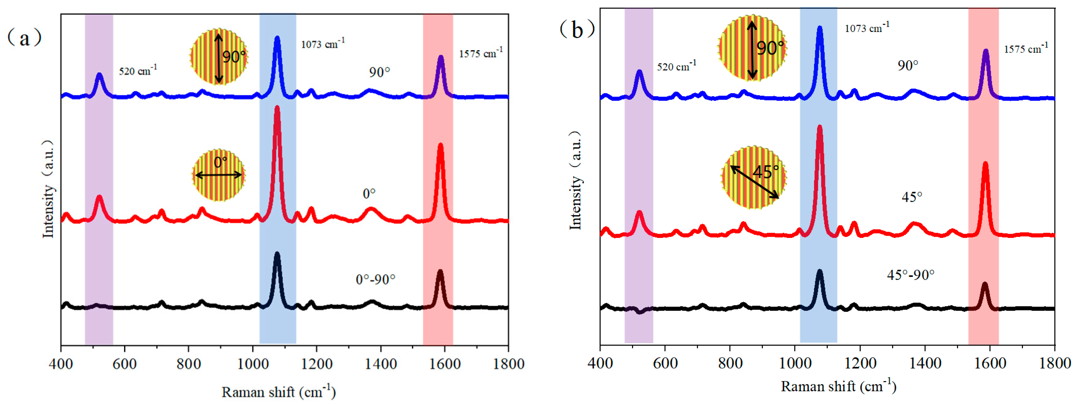
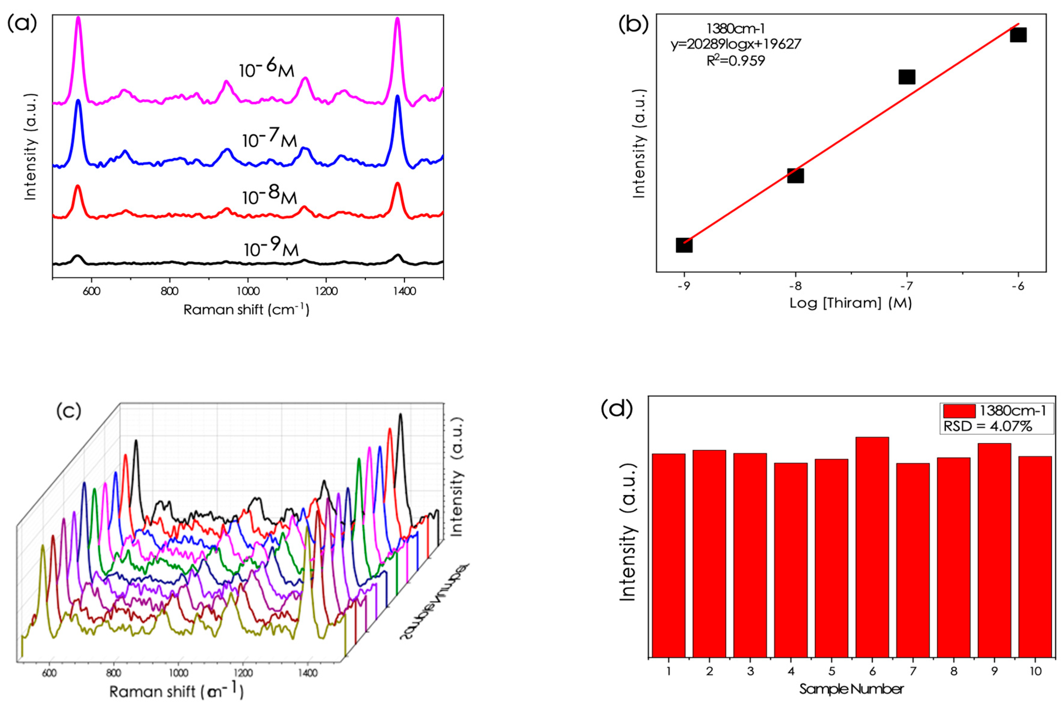
The FDTD lumerical is chosen for the simulation of the electromagnetic field distribution in the prepared nanostructure. The regularly arranged nanorods are arranged in the X–Y plane and perpendicular to the X–Z plane. The dielectric constant and permeability values of Ag given by the FDTD software are used in the simulation. The refractive index of the PS spheres is set as 1.585. The radius of the PS spheres is identified as 500 nm. With a change in the first magnetron sputtering time, the sparsity of the silver nanoparticles in the middle of the PS sphere also changed, which also lead to a change in the size and gap of the regular nanorods after etching. In response to the different etching times, the radius of the nanorods and the distance between nanorods changed. A grid size of 1 nm was chosen, and a conformal variant of 2 was set for mesh refinement. The simulation time was set to 1000 s overall, and the minimum value for auto shutoff was set as 1 × 10⁻⁵. The simulation temperature was set to 300 K. The permittivity and permeability for the Au were obtained from the material database of the lumerical FDTD software.

3. Results

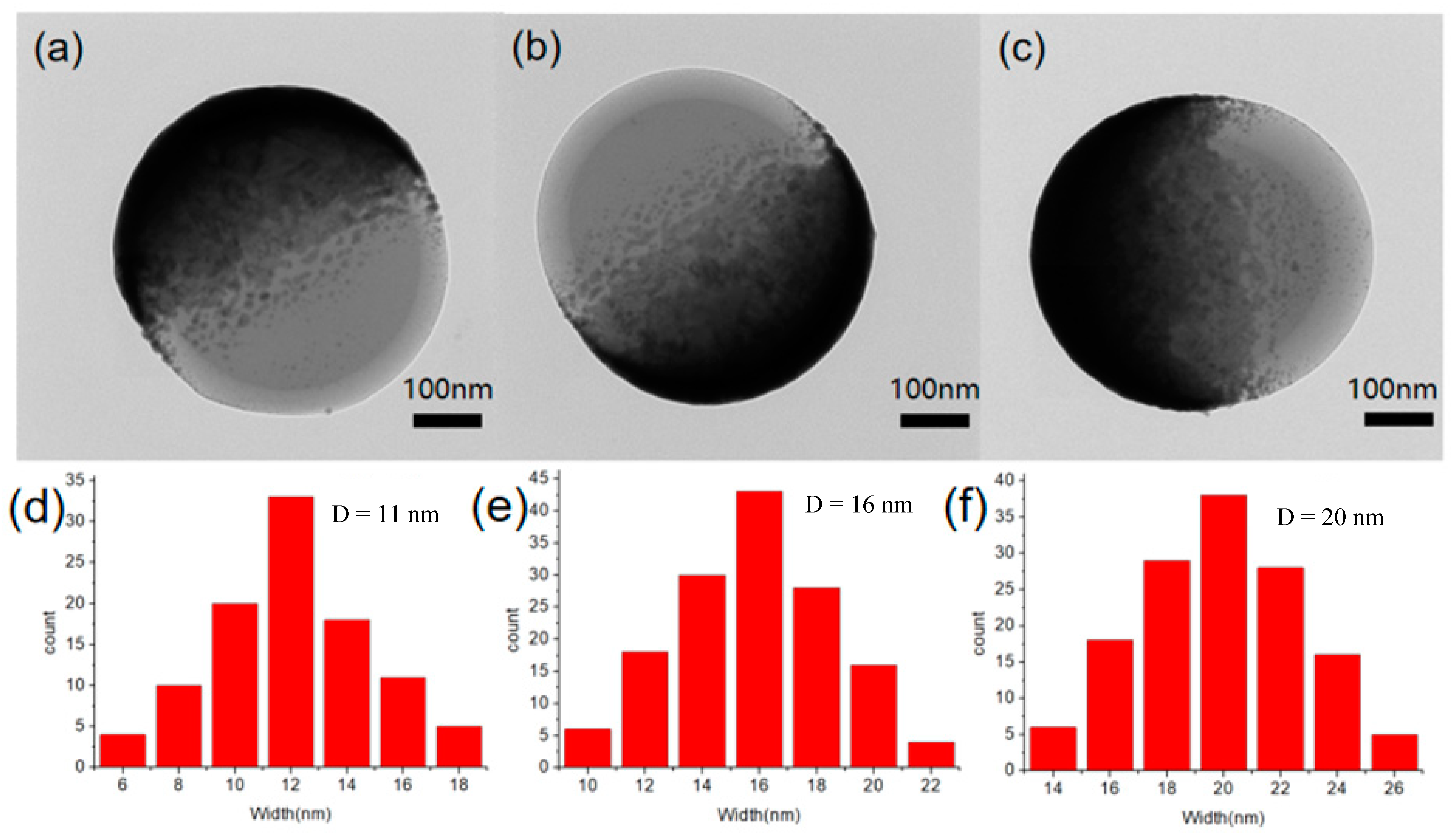
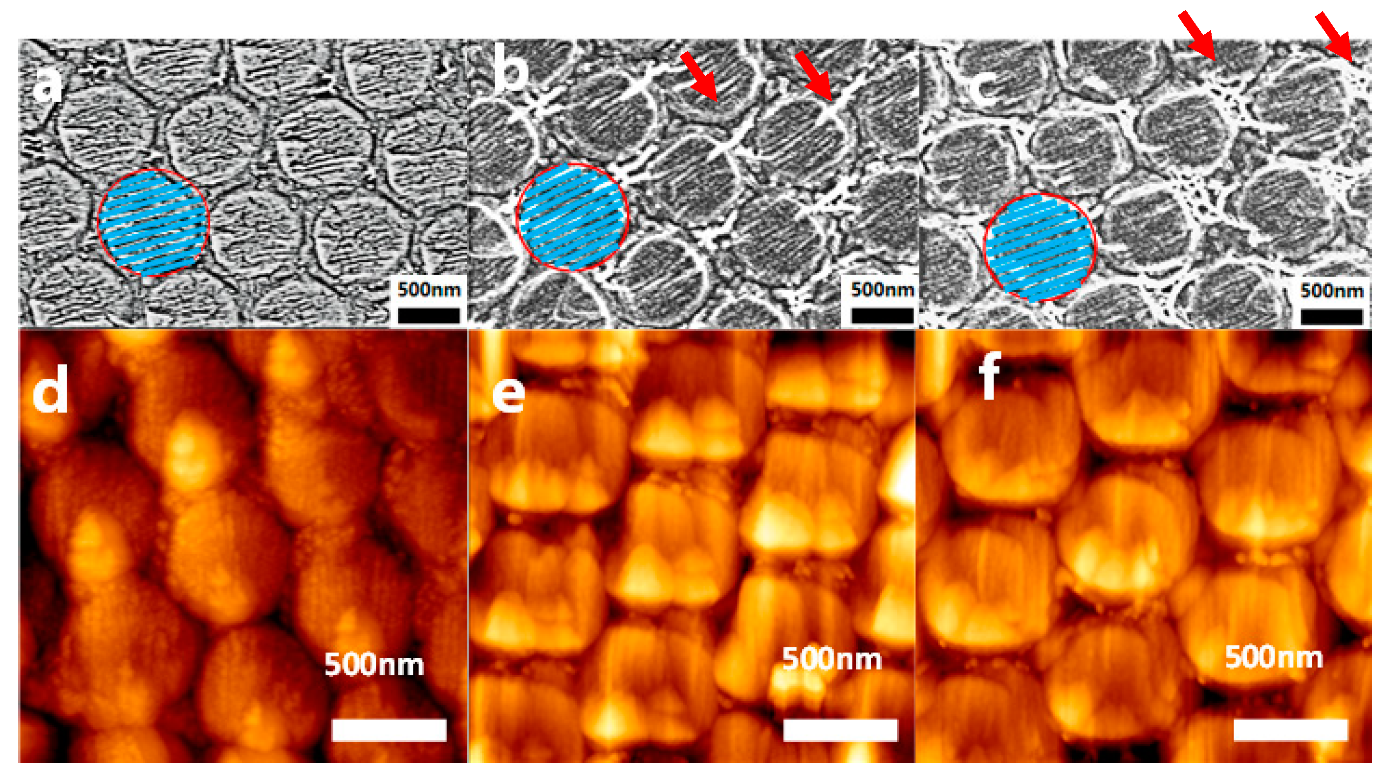
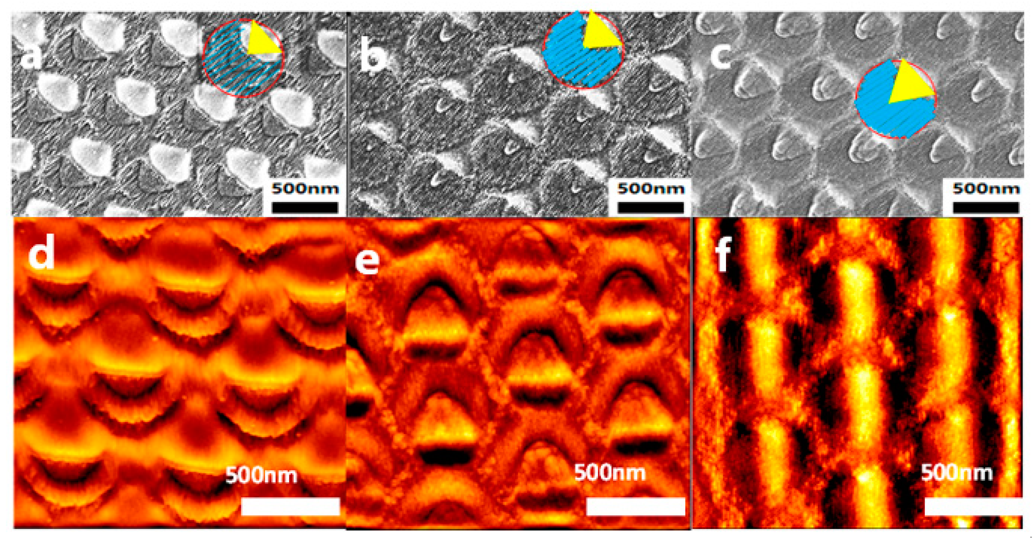
3.1. Microstructure Characterization

Based on two-dimensional 500 nm self-assembled PS arrays, the nanorod fabrication is illustrated in Figure 1. First, a PS array with a size of 500 nm is self-assembled on a Si substrate, which forms a two-dimensional closely compact pattern with a period equal to the PS sphere diameter of 500 nm. Second, Ag films with different thickness are sputtered onto PS sphere arrays by magnetron control sputtering, which forms a nanocap on the PS sphere with some scattered Ag nanoparticles along the nanocap brim. Third, the PS arrays along with Ag film arrays are transferred onto a new substrate by double-sided sticky tape with the PS spheres facing up. Fourth, ion etching is performed on the PS arrays with Ag nanoparticles used as a mask. Etched by the high-speed argon ion, parallel PS nanorods form on PS because of the shielding effects of Ag nanoparticles on one end, as shown in Figure 1d. To get samples with different surface morphologies, the etching angle between the ion beam and the substrate surface is set as 15° and 30°, respectively.
When Ag film is deposited onto a PS sphere array by the magnetron control sputtering process, the curved film forms nanocap shapes that are observed on the PS spheres. The top part of the curved film is continuous due to its large thickness, and some scattered Ag nanoparticles are observed around the brim of the curved film due to its small thickness, as shown in the TEM images (Figure 2). The analysis of the size distribution of Ag nanoparticles shows that the Ag nanoparticle size around the brim of the curved film increases with the deposition time. The film thickness decreases along the PS surface to the film brim, which leads to Ag nanoparticles with decreased sizes. The analysis of the Ag nanoparticle size distribution shows that the average diameter of the nanoparticles is D = 11 nm for a deposition time of 60 s. When the sputtering time is 90 s, the Ag film becomes thick and Ag nanoparticles grow to D = 16 nm. With an increase in sputtering time to 120 s, the average size of the Ag nanoparticles is D = 20 nm.
When tilted ion etching is performed with an obliquity angle of 15°, the top part of the PS sphere is etched away first and the PS surfaces become flat gradually. PS nanorods are observed to lie on each PS sphere due to the shielding effects of Ag nanoparticles. During the etching process, the Ag ions fly in the same direction under the same accelerating voltage, and the PS spheres are etched in the same way, which results in the PS nanorods being parallel to each other in spite of the Ag nanoparticles being distributed along the curved surface. Figure 3 shows the SEM and AFM images of Ag-covered nanorods for Ag sputtering times of 60 s, 90 s, and 120 s. The closely aligned nanorods are observed to be arranged in the same direction as guided by the red circles, which show that the sample is composed of many domains and that each domain contains many parallel nanorods. During the etching procedure, some nanorods are observed off the domains, as shown by the red arrows, which confirm the formation of the nanorods. SEM images show the size distributions for the nanorod diameter and the space size between the neighboring nanorods for different Ag growth times, which show that the increasing growth time results in increased nanorod diameters and decreased space sizes between the neighboring nanorods. When Ag nanoparticles with a sputtering time of 60 s are used as the mask, the diameter of the nanorods is about 10 nm, and the space between the nanorods is about 20 nm. When Ag nanoparticles with a sputtering time of 90 s are used as the mask, the diameter of the nanorods is about 15 nm, and the space between the nanorods is about 15 nm. When the sputtering time of the masking Ag nanoparticles is increased to 120 s, the diameter of the nanorods increases to 20 nm and the space between the nanorods decreases to 10 nm. The results above show that the increased sputtering time leads to the large diameter of the aligned nanorods and the small space between the nanorods, which is attributed to the protection provided by large Ag nanoparticles with increasing growth time. During the etching process with an obliquity angle of 15°, the upper part of the PS spheres is gradually etched by argon ions, and the bottom part is left unetched due to the protection of Ag film. For the middle part of the PS beads around the brim of the Ag cap, the scattered Ag nanoparticles will act as a mask shielding the etching process, which leads to a PS nanorod formation. Due to the consistent direction of the ion beam, all nanorods show the same direction for all PS spheres on the substrate, even for PS spheres in different domains or out of domains. Due to the high consistency of the prepared nanorods, random points can also be taken as samples for self-reference detection to remove background noise. For comparison, an etching angle of 30° is also chosen for the fabrication of Ag nanorod arrays as shown in Figure 4, which results in quite different surface morphologies. Different from the sample with an etching angle of 30°, the protruding formation of a triangle shape is observed on each PS bead. When the etching angle increases, self-shadow effects are observed due to the curved surfaces, and the shadow effects from the front PS beads are also increased, which results in a reduced etching rate due to the front partial PS beads. As the etching time increases, the heights of the protruded parts decrease, and the shielding effects also decrease.

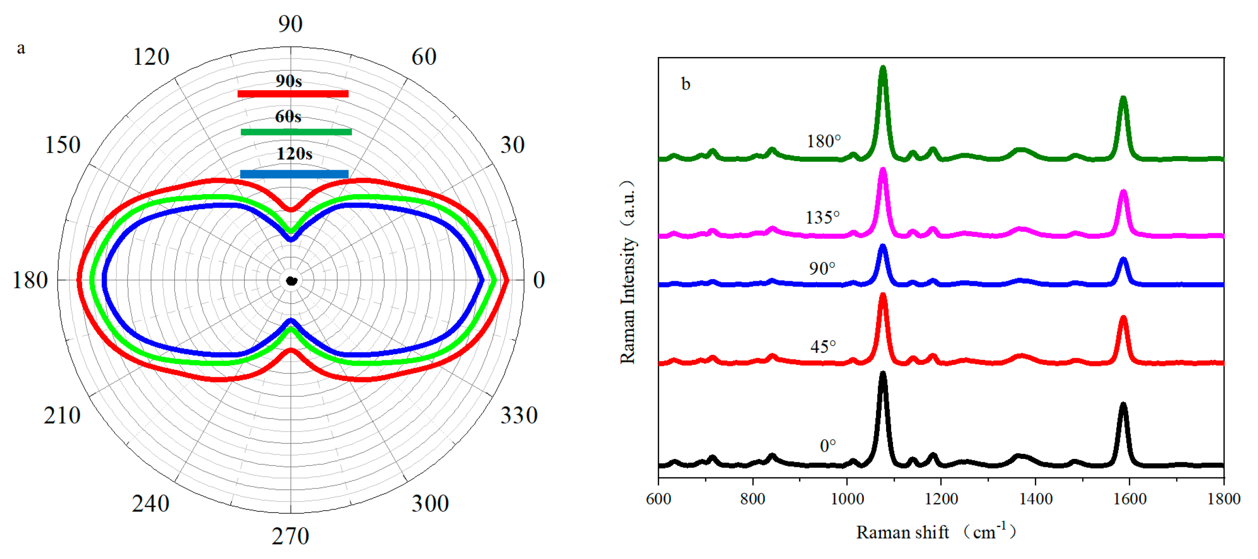
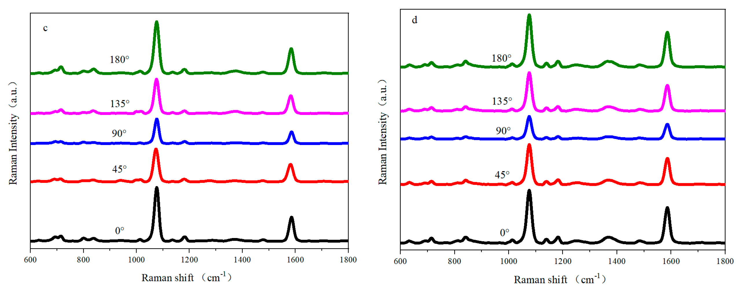
3.2. Optical Properties
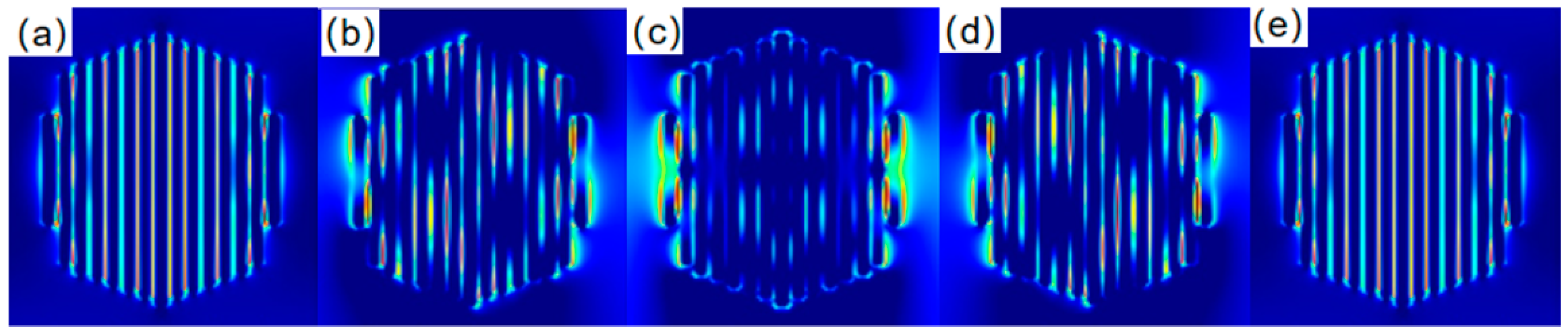
When a Ag film of thickness 5 nm is deposited onto the PS nanorod array with the same deposition parameters as mentioned above, the etching process results in aligned Ag nanorods with different diameters and distances, which depend on the structural parameters of the PS nanorods. Obvious polarization properties are observed for Ag nanorods, and the large aspect ratio and small nanogap between Ag nanorods lead to the strong electromagnetic coupling. The polarization property of the SERS substrate is investigated using angular SERS measurements with 4-MBA as the probe molecule, in which the sample is rotated horizontally to change the angles between the electric field direction and nanorod direction as shown in Figure 5a. The laser with a wavelength of 785 nm is used as the excitation source for the Raman measurements, and the characteristic SERS peaks are obtained for the 4-MBA molecule. The peak at 1073 cm−1 is due to the symmetric C-H in-plane bending and C-S stretching. The peak at 1575 cm−1 is due to the ring C-C stretching and asymmetric C-H in-plane bending, and the intensity of signal changes obviously with polarization angle. The remaining characteristic peaks are summarized in Table 1. In addition, the peak at 520 cm−1 shows no change in intensity with polarization angle, which is assigned to the background peak of the silicon wafer, providing a good reference peak for all samples. Figure 5a shows the pole diagram of the intensity of the characteristic peak at 1073 cm−1, which shows good angle-dependent behaviors for the nanorod array. When the electrical vector, E, is vertical to the nanorod array, that is, when the measurement angle is 0°, the characteristic peaks show the largest intensity. When the measurement angle increases, the SERS intensity decreases, and the smallest intensity is reached when the electrical vector, E, is parallel to the nanogaps between the Ag nanorods. It is well known that background signals are the main disadvantageous factor for SERS signals due to the absorbed impurity molecules, background fluorescence, non-uniform distribution of the substrate, and so on. In our structure, the characteristic signals change with the detection polarization angle, but the background signals show no changes, which indicates that the background signals are independent from the polarization property of the nanorod structure. In comparison with the sample sputtering times of 60 s and 120 s, the nanorod array with a sputtering time of 90 s has a good SERS polarization performance, as shown in Figure 5.
To improve the quality of the SERS spectra, the polarization property is used as a self-reference to eliminate the effects of the background signals. When SERS characterization is performed, the signal for the peak at 520 cm−1 from the Si substrate is also detected, which is from the substrate outside the PS coverage. When the PS sphere is etched with etching angles of 15° and 30°, the PS coverage area shows no changes, which results in a maintained intensity for the substrate peak at 520 cm−1. In addition, the peak at 520 cm−1 is independent from the light polarization, and no peak shift and peak intensity change is observed when the substrate is rotated during Raman measurement. Therefore, the peak at 520 cm−1 from the substrate Si is used as the reference. To obtain improved SERS signals, a subtracted Raman spectrum is obtained by subtracting the spectrum measured at an angle of 0° from the spectrum measured at angle 90°, and the expected operation means that the Si peak is decreased to zero for the subtraction spectrum, as shown in Figure 6a. Figure 6b shows the subtraction of the Raman spectrum with a measurement angle of 90° from the Raman spectrum with a measurement angle of 45°, which shows that Raman intensity after eliminating the background is still observed. When the peak at 520 cm−1 is eliminated, the characteristic peak of the detected molecule is still preserved because the SERS peak intensity is reduced for a measurement angle of 45°.

3.3. FDTD Analysis

In order to study the dependence of electromagnetic enhancement on the modification of regular silver nanorods and the direction of laser polarization, FDTD simulation is used to carry out numerical simulations for the local electric field distribution of regular silver nanorod arrays. Due to the large distance, the electromagnetic coupling between the neighbor units is weak in comparison to the coupling between the nanorods on each PS sphere. Therefore, the silver nanorods on a single PS sphere are selected as the minimum computing unit. The electromagnetic field distribution and hot spots are calculated by adjusting the spacing between silver nanorods in the minimum computational structure. The hot spot distributions in Figure 7 show that the hot spots are mainly distributed in the gap between the silver nanorods. When the electric field direction is perpendicular to the silver nanorods, the hot spots are mainly distributed in the gap between the nanorods and the intensity increases. When the electric field direction rotates 45 degrees from the silver nanorods, the hot spot area between the silver nanorods decreases and the intensity becomes weak. When the electric field is parallel to the silver nanorods, the hot spots are mainly concentrated at both ends of the nanorod, but the electromagnetic couplings between the neighboring nanorods are decreased greatly. These observations confirm that the electromagnetic coupling has an angular dependence, revealing the physical root for the angular dependence of SERS observations.
For a good performance of the SERS substrate composed of a Ag-covered nanorod array, it is used to detect thiram after the Ag-covered nanorod array is immersed in the thiram solution at different concentrations: 10−6 M, 10−7 M, 10−8 M, and 10−9 M. As shown in Figure 8a, the intensity of the SERS peaks decreases with the decrease in thiram concentrations, and the SERS substrate still works when the thiram concentration is down to 10−9 M, which is below the concentration standard set by the U.S. Environmental Protection Agency, indicating its suitable application in the fields of food safety and environmental protection. The strongest peak at 1380 cm−1 is attributed to CN stretching and CH3 symmetry, and the second strongest peak at 560 cm−1 is attributed to a C-S-S asymmetric stretching vibration. The peak at 930 cm−1 is attributed to C=S stretching and CH3N, and the peak at 1138 cm−1 is attributed to CN stretching and the CH3 rocking modes. These observations show that the localized electromagnetic field is enhanced for different vibration modes, which gives us many choices for quantity analysis. For different thiram concentrations, these SERS observations show no changes in peak positions, and the peak intensities show obvious changes. To build the relationship between the intensity of the Raman peak and the thiram concentration, a function between the intensity of the characteristic peak at 1380 cm−1 and the logarithm of the extract concentration is fitted as y = 20,289 logx + 19,627, R2 = 0.959, where x is the logarithm of the thiram concentrations and y is the intensity of the peak at 1380 cm−1, as shown in Figure 8b. The linear dependence between x and y confirms the possible prediction of thiram concentration based on the changed intensity of the SERS peak at 1380 cm−1. In addition to the high sensitivity, the uniformity of the SERS substrate is another key parameter for reliable SERS detection, which ensures the reproducibility of the signals for different positions. The SERS spectra are collected by randomly selecting 10 points throughout the sample. Figure 8c shows that all the selected spots show almost identical SERS signals, and the intensity and the position of the characteristic peaks are observed to be the same. The columnar chart in Figure 8d shows the intensity of the characteristic peak at 1380 cm−1, and the relative standard deviation is calculated to be 4.07% for 10 random points, which also confirms the good repeatability of the SERS observations.

4. Conclusions

In this work, we prepared a SERS substrate of Ag nanorods based on a PS array by sputtering Ag and ion etching. When the scattered Ag nanoparticles around the nanocap brim are used as the mask materials, parallel PS nanorods are created on each PS sphere, and each PS sphere is a polarized domain when Ag is deposited to form Ag nanorods by covering the PS nanorods. The SERS substrate is composed of many working domains which contain many parallel Ag nanorods, and all SERS domains show the same polarization properties. By controlling the magnetic sputtering time, the diameters of the Ag nanorods and the electromagnetic coupling between the Ag nanorods are controlled, as verified by FDTD simulation. When ion etching with an etching angle of 30° is applied to the PS array with a sputtering time of 90 s and Ag nanoparticles as the mask, Ag nanorods are obtained with a diameter of 15 nm and a spacing of 15 nm. Due to the highly polarized SERS spectrum from this substrate, the noises in the SERS spectra are removed through a self-reference method, which leads to a high sensitivity and excellent reliability for the thiram detection, and the concentration limit for detection is as low as 10−9 M. Compared with other techniques, our nanorods show the excellent behavior of the polarized SERS for each PS sphere, even if the PS spheres are outside the ordered array, which makes great contributions to the development of the design and fabrication of SERS substrates.

Author Contributions

Conceptualization, X.Z. and Y.Z.; software, R.G., S.Z. and Y.Z.; formal analysis, D.M., R.G. and Y.W. (Yuxia Wang); writing—original draft preparation, D.M., Y.W. (Yaxin Wang) and Y.Z.; writing—review and editing, X.Z., D.M., Y.W. (Yaxin Wang) and X.G.; supervision, X.Z. and Y.W.; project administration, X.Z. and Y.W. (Yaxin Wang); funding acquisition, X.Z. All authors have read and agreed to the published version of the manuscript.

Funding

This work is supported by the National Natural Science Foundation of China (Nos. 51901060, 12004090); the National Natural Science Foundation of Zhejiang Province (Nos. LY21E010004, LQ21A040009); the Fundamental Research Funds for the Provincial Universities of Zhejiang (No. GK239909299001-007, GK209907299001–025); the Key Research Project of Zhejiang Lab (Nos. 2022MH0AC01, 2022MG0AB02).

Institutional Review Board Statement

Not applicable.

Informed Consent Statement

Informed consent was obtained from all subjects involved in the study.

Data Availability Statement

This study did not report any data.

Conflicts of Interest

The authors declare no conflict of interest.

References

  1. Linic, S.; Aslam, U.; Boerigter, C.; Morabito, M. Photochemical transformations on plasmonic metal nanoparticles. Nat. Mater. 2015, 14, 567–576. [Google Scholar] [CrossRef] [PubMed]
  2. Kherbouche, I.; Luo, Y.; Félidj, N.; Mangeney, C. Plasmon-Mediated surface functionalization: New horizons for the control of surface chemistry on the nanoscale. Chem. Mater. 2020, 32, 5442–5454. [Google Scholar] [CrossRef]
  3. Chen, W.; Shi, H.; Wan, F.; Wang, P.; Gu, Z.; Li, W.; Huang, Y. Substrate influence on the polarization dependence of SERS in crossed metal nanowires. J. Mater. Chem. C 2017, 5, 7028–7034. [Google Scholar] [CrossRef]
  4. Lee, H.; Kim, G.H.; Lee, J.H.; Kim, N.H.; Nam, J.M.; Suh, Y.D. Quantitative plasmon mode and Surface-Enhanced Raman Scattering analyses of strongly coupled plasmonic nanotrimers with diverse geometries. Nano Lett. 2015, 15, 4628–4636. [Google Scholar] [CrossRef] [PubMed]
  5. Tumkur, T.U.; Yang, X.; Cerjan, B.; Halas, N.J.; Nordlander, P.; Thomann, I. Photoinduced force mapping of plasmonic nanostructures. Nano Lett. 2016, 16, 7942–7949. [Google Scholar] [CrossRef] [PubMed]
  6. Vasista, A.B.; Jog, H.; Heilpern, T.; Sykes, M.E.; Tiwari, S.; Sharma, D.K.; Kumar, G.V.P. Differential wavevector distribution of Surface-Enhanced Raman Scattering and fluorescence in a film-coupled plasmonic nanowire cavity. Nano Lett. 2017, 18, 650–655. [Google Scholar] [CrossRef]
  7. Pal, S.; Harmsen, S.; Oseledchyk, A.; Hsu, H.T.; Kircher, M.F. MUC1 aptamer targeted SERS nanoprobes. Adv. Funct. Mater. 2017, 27, 1606632. [Google Scholar] [CrossRef]
  8. Wang, X.; Guo, L. SERS activity of semiconductors: Crystalline and amorphous nanomaterials. Angew. Chem. Int. Ed. 2019, 59, 4231–4239. [Google Scholar] [CrossRef]
  9. Tian, Y.; Wang, H.; Yan, L.; Zhang, X.; Falak, A.; Guo, Y.; Chu, W. A generalized methodology of designing 3D SERS probes with superior detection limit and uniformity by maximizing multiple coupling effects. Adv. Sci. 2019, 6, 1900177. [Google Scholar] [CrossRef]
  10. McLellan, J.M.; Li, Z.; Siekkinen, A.R.; Xia, Y. The SERS activity of a supported Ag nanocube strongly depends on its orientation relative to laser polarization. Nano Lett. 2007, 7, 1013–1017. [Google Scholar] [CrossRef]
  11. Zhang, L.; Sun, J.; Li, Z.; Yuan, Y.; Liu, A.; Huang, Y. Coherent enhancement of dual-path-excited remote SERS. ACS Appl. Mater. Interfaces 2020, 12, 32746–32751. [Google Scholar] [CrossRef] [PubMed]
  12. Zhang, B.Y.; Yin, P.; Hu, Y.; Szydzik, C.; Khan, M.W.; Xu, K.; Thurgood, P.; Mahmood, N.; Dekiwadia, C.; Afrin, S.; et al. Highly accurate and label-free discrimination of single cancer cell using a plasmonic oxide-based nanoprobe. Biosens. Bioelectron. 2021, 198, 113814. [Google Scholar] [CrossRef]
  13. Alsaif, M.M.Y.A.; Haque, F.; Alkathiri, T.; Krishnamurthi, V.; Walia, S.; Hu, Y.; Jannat, A.; Mohiuddin; Xu, K.; Khan, M.W.; et al. 3D Visible-Light-Driven Plasmonic Oxide Frameworks Deviated from Liquid Metal Nanodroplets. Adv. Funct. Mater. 2021, 31, 2106397. [Google Scholar] [CrossRef]
  14. Bai, S.; Serien, D.; Hu, A.; Sugioka, K. 3D Microfluidic Surface-Enhanced Raman Spectroscopy (SERS) Chips Fabricated by All-Femtosecond-Laser-Processing for Real-Time Sensing of Toxic Substances. Adv. Funct. Mater. 2018, 28, 1706262. [Google Scholar] [CrossRef]
  15. Zhang, D.; Xia, C.; Li, S.; Liu, H.; Ding, L.; Liu, X.; Li, Y. Detection of off-resonance single-walled carbon nanotubes by enormous Surface-Enhanced Raman Scattering. Adv. Opt. Mater. 2021, 9, 2100559. [Google Scholar] [CrossRef]
  16. Langer, J.; Jimenez, D.; Aizpurua, J.; Alvarez, R.A.; Auguie, B.; Baumberg, J.J.; Liz-Marzan, L.M. Present and future of Surface-Enhanced Raman Scattering. ACS Nano 2020, 14, 28–117. [Google Scholar] [CrossRef]
  17. Wei, H.; Hao, F.; Huang, Y.; Wang, W.; Nordlander, P.; Xu, H. Polarization dependence of Surface-Enhanced Raman Scattering in gold nanoparticle-nanowire systems. Nano Letter 2008, 8, 2497–2502. [Google Scholar] [CrossRef]
  18. Lee, S.Y.; Hung, L.; Lang, G.S.; Cornett, J.E.; Mayergoyz, I.D.; Rabin, O. Dispersion in the SERS Enhancement with Silver Nanocube Dimers. ACS Nano 2010, 4, 5763–5772. [Google Scholar] [CrossRef]
  19. Tian, C.; Ding, C.; Liu, S.; Yang, S.; Song, X.; Ding, B.; Li, Z.; Fang, J. Nanoparticle Attachment on Silver Corrugated-Wire Nanoantenna for Large Increases of Surface-Enhanced Raman Scattering. ACS Nano 2011, 5, 9442–9449. [Google Scholar] [CrossRef]
  20. Eom, G.; Kim, H.; Hwang, A.; Son, H.Y.; Choi, Y.; Moon, J.; Kim, B. Nanogap-rich Au nanowire SERS sensor for ultrasensitive telomerase activity detection: Application to gastric and breast cancer tissues diagnosis. Adv. Funct. Mater. 2017, 27, 1701832. [Google Scholar] [CrossRef]
  21. Pissuwan, D.; Hattori, Y. Detection of Adhesion Molecules on Inflamed Macrophages at Early-Stage Using SERS Probe Gold Nanorods. Nano-Micro Lett. 2016, 9, 8–17. [Google Scholar] [CrossRef] [PubMed]
  22. Niu, R.; Song, C.; Gao, F.; Fang, W.; Jiang, X.; Ren, S.; Zhu, D.; Su, S.; Chao, J.; Chen, S.; et al. DNA Origami-Based Nanoprinting for the Assembly of Plasmonic Nanostructures with Single-Molecule Surface-Enhanced Raman Scattering. Angew. Chem. Int. Ed. 2021, 60, 11695–11701. [Google Scholar] [CrossRef] [PubMed]
  23. Andrea, C.D.; Bochterle, J.; Toma, A.; Huck, C.; Neubrech, F.; Messina, E.; Fazio, B.; Marago, O.M.; Fabrizio, E.D.; Chapelle, M.; et al. Optical nanoantennas for multiband surface-enhanced infrared and raman spectroscopy. ACS Nano 2019, 494, 87–93. [Google Scholar]
  24. Hao, N.; Pei, Z.; Liu, P.; Bachman, H.; Naquin, T.D.; Zhang, P.; Huang, T.J. Acoustofluidics-assisted fluorescence-SERS bimodal biosensors. Small 2020, 16, 2005179. [Google Scholar] [CrossRef]
  25. Cheng, M.; Zhang, F.; Zhu, A.; Zhang, X.; Wang, Y.; Zhao, X.; Zhang, X. Bridging the neighbor plasma coupling on curved surface array for early hepatocellular carcinoma detection. Sens. Actuators B Chem. 2020, 309, 127759. [Google Scholar] [CrossRef]
  26. Kasani, S.; Curtin, K.; Wu, N. A review of 2D and 3D plasmonic nanostructure array patterns: Fabrication, light management and sensing applications. Nanophotonics 2019, 8, 2065–2089. [Google Scholar] [CrossRef]
  27. Zhu, Q.; Zhao, X.; Zhang, X.; Zhu, A.; Gao, R.; Zhang, Y.; Chen, L. Au nanocone array with 3D hotspots for biomarker chips. CrystEngComm 2020, 22, 5191–5199. [Google Scholar] [CrossRef]
  28. Zhu, A.; Zhang, F.; Gao, R.; Zhao, X.; Chen, L.; Zhang, Y.; Wang, Y. Increasing polarization-dependent SERS effects by optimizing the axial symmetry of plasmonic nanostructures. Appl. Surf. Sci. 2019, 494, 87–93. [Google Scholar] [CrossRef]
  29. Gao, R.; Zhang, Y.; Zhang, F.; Guo, S.; Wang, Y.; Chen, L.; Yang, J. SERS polarization-dependent effects for an ordered 3D plasmonic tilted silver nanorod array. Nanoscale 2018, 10, 8106–8114. [Google Scholar] [CrossRef]
  30. Agrawal, A.; Cho, S.H.; Zandi, O.; Ghosh, S.; Johns, R.W.; Milliron, D.J. Localized Surface Plasmon Resonance in semiconductor nanocrystals. Chem. Rev. 2018, 118, 3121–3207. [Google Scholar] [CrossRef]
  31. Mao, D.; Zhao, X.; Wen, J.; Wang, A.; Gao, R.; Wang, Y. Enhanced Electromagnetic Coupling in the Walnut-Shaped Nanostructure Array. Chemosensors 2022, 10, 445. [Google Scholar] [CrossRef]
Figure 1. Schematic diagram for the preparation of a SERS substrate composed of Ag nanorod array. (a) Ordered PS beads array by self-assembly technique; (b) Ag sputtered onto PS array with separated Ag nanoparticles around the film brim; (c) PS arrays along with Ag film arrays are transferred onto a new substrate; (d) PS nanorods formation after ion etching due to the shielding effects of Ag nanoparticles.
Chemosensors 11 00462 g001
Figure 2. TEM images of the PS spheres with different thickness Ag films after sputtering for (a) 60 s, (b) 90 s, and (c) 120 s, and the corresponding histograms of the Ag nanoparticle size (df).
Chemosensors 11 00462 g002
Figure 3. SEM and AFM images of the Ag-covered nanorods after an etching time of 30 min under an etching obliquity of 15° for different Ag film sputtering times: 60 s (a,d), 90 s (b,e), and 120 s (c,f). The blue lines show the Ag nanorods. The red arrows show the nanorods out of the array.
Chemosensors 11 00462 g003
Figure 4. SEM and AFM images of the Ag nanorods with an etching angle of 30° for different sputtering times of (a,d) 60 s, (b,e) 90 s, (c,f) 120 s. The red circles show the PS beads, the blue lines show the nanorods and the triangles show the protrude parts left.
Chemosensors 11 00462 g004
Figure 5. For Ag nanorods obtained with an etching angle of 30°, the SERS spectra show the angular dependence when excited by the polarized light. (a) when 4-MBA molecules are adsorbed on for Ag sputtering times of 60 s (b), 90 s (c), and 120 s (d). The lines with different colors in Figure 5 (a) show different times for Ag sputtering 60 s, 90 s, and 120 s. The lines with different colors in Figure 5(bd) show the measurement angles 0°, 45°,90°, 135°, and 180°.
Chemosensors 11 00462 g005aChemosensors 11 00462 g005b
Figure 6. Raman diagram of the nanorod array with a sputtering time of 90 s, (a) Raman spectra for the measurements with electric field angles of 90° and 0° in the nanorod array. (b) Raman spectra for the measurements with electric field angles of 45° and 0° in the nanorod array.
Chemosensors 11 00462 g006
Figure 7. FDTD simulations of the electromagnetic field distribution and hot spots for different etching samples (ae) the Ag nanorods when the sputtering time is 90 s and the etching time is 40 min, (a) 0°, (b) 45°, (c) 90°, (d) 135°, (e) 180°.
Chemosensors 11 00462 g007
Figure 8. (a) SERS spectra of the thiram with different concentrations, 10−6 M, 10−7 M, 10−8 M, and 10−9 M. (b) The relationship between the signal intensity at 1380 cm−1 of the thiram and the corresponding logarithmic concentration. (c) The SERS spectra from 10 randomly selected points. (d) SERS intensity distribution of the thiram peak at 1380 cm−1 from 10 randomly selected points.
Chemosensors 11 00462 g008
Table 1. Chemical bond of the remaining characteristic peaks of 4-MBA for SERS spectra.
Raman Shift (cm−1)Vibrational Modes
719γ(CCC) out-of-plane ring vibration
846δ(COO-) bending vibration
1296Ring in-plane C-H bending mode
1318C-O stretching mode
Disclaimer/Publisher’s Note: The statements, opinions and data contained in all publications are solely those of the individual author(s) and contributor(s) and not of MDPI and/or the editor(s). MDPI and/or the editor(s) disclaim responsibility for any injury to people or property resulting from any ideas, methods, instructions or products referred to in the content.

