Abstract
Multi-level inverters are widely employed to generate new energy because of their huge capacity and benefits in sound control performance. One of the critical areas of study for multi-level inverters is control strategy research. In this study, the control strategy for a multi-level inverter—which is frequently employed in HVDC and FACTS systems—is designed. An asymmetrical D.C. voltage source is supplied to create the appropriate output voltage waveform with fewer total harmonic distortions (THDs) at the output voltage and current waveforms. In this work, the pulse width modulation techniques of POD (phase opposition disposition) and APOD (alternative phase opposition disposition) MC PWM are applied to a multi-level inverter to generate the seven-level output voltage waveform. This study presents an enhanced variable carrier frequency APOD control approach that can successfully lower the overall harmonic distortion rate. The design and completion of the phase-shifting POD and APOD control strategies are followed by an analysis and comparison of the THD situation under various switching frequencies and a simulation and verification of the control strategy using MATLAB simulation. The TI DSP-based control approach has been programmed. The APOD technique increases the output voltage’s THD to 18.27%, while the output current waveform’s THD is reduced to 15.67% by utilizing the APOD PWM technique. Using the POD PWM approach increases the total harmonic distortion (THD) of the voltage waveform by 18.06% and the output current waveform’s THD by 15.45%.
MSC:
65T50
1. Introduction
A multi-level inverter is a power electronic system that uses a low-level D.C. voltage as input to provide the required A.C. voltage output. As a new type of high-power inverter, the multi-level inverter can generate high voltage and reduce harmonics through its circuit topology. Therefore, multi-level voltage source converters often appear in high-power applications [1]. Multi-level voltage source converters synthesize stepped voltage waves from several D.C. capacitive voltages. One of the significant limitations of multi-level converters is the voltage imbalance between different levels. Techniques for balancing voltages between different levels usually include voltage clamping or capacitive charging control [2]. There are many ways to achieve voltage balance in multi-level converters. The sum of the inverter’s output voltage is equal to the output voltage of the M-class inverter. The difference lies in the multi-level inverter’s switching mechanism and the input voltage’s source [3].
Traditional two and three-level inverters have many limitations when dealing with high voltage and power conversion. With a higher capacity and reduced output voltage harmonic distortion, the converter is connected in series with the transformer. This is assumed to be the primary harmonic elimination method of the multi-level inverter; the improvement of power quality is also crucial to researching and comparing different topologies of pulse width modulation [4]. The international community currently relies heavily on non-renewable energy, but after the recent oil crisis, increasing the use of renewable energy has become a top priority for many countries due to its numerous benefits, including minimal environmental impact. Unlike conventional generators, renewable energy needs less maintenance and has a significant economic effect [5]. Today, the electronic world is a global society. In the future, industrial society will be led by two technologies: highly automated computers and power electronics. Multi-level inverters are commonly used in various industries. Applications include hybrid active harmonic filters, reactive power compensation, traction, electric vehicles, single-phase and three-phase induction motor speed control, and more [6]. They are also used in the renewable energy sector. In recent years, electrical engineering researchers have paid attention to multi-level inverters in many industrial applications in terms of quality and reliable power [7]. To improve the efficiency of solar photovoltaic energy conversion systems, a multi-level inverter was developed as a viable alternative to traditional straight-beam transducer renewable energy systems [8].
The multi-level inverter (MLI) has become a fascinating and powerful DC–AC converter among various inverter schemes. In many power electronics applications, the MLI has been a significant research area in power electronics in recent years because of its advantages, such as low switching loss, strong voltage operation ability, high efficiency, low voltage, and slight electromagnetic interference. A novel topology for the multi-level inverter based on the series connection of basic modules has been developed. The suggested topology is utilized for symmetrical and asymmetric source systems, which can be used for fuel cell and photovoltaic systems [9]. A new multi-level inverter topology employing the concept of half-bridge modules is suggested in this paper. It requires a lower number of DC sources and power components. The inverter is controlled using a fundamental frequency-switching scheme [10]. The proposed control strategy simplifies the design of the control system, reduces the computational burden, and can be easily extended to MMC with any S.M. number [11]. In this study, equations for combining different pulse width modulation (PWM) techniques to use the controllability advantage of the multi-carrier method are introduced in asymmetric topologies [12]. The proposed study suggests the application of a whale optimization algorithm (WOA) based on a fractional-order proportional-integral controller (FOPIC) for unified power quality conditioner (UPQC) and STATCOM tools; furthermore, since the output is similar to sinusoidal waves, it has the benefits of good power efficiency, low harmonic distortion, and low EMI [13].
The lower-order harmonics in the inverters and modulation techniques highly affect the performance and efficiency of the system and are suitable for PWM, which is used to control and mitigate these effects. Currently, most inverters seem to be quasi-square wave inverters with a lot of distortion. Researchers are working hard to create and commercialize effective, distortion-free inverters [14]. Low cost, reduced switching complexity, and efficient filtering are also priorities in inverter architecture. While single-pole and bipolar inverters are well-known, much room remains for improvement [15].
Table 1 provides a descriptive and critical table summary of the literature review showing the research gaps.

Table 1.
Descriptive and critical table summary of the literature review.
The main contributions of the paper are as follows:
- A cascaded H-bridge multi-level inverter performs much better than the traditional two-level inverter because it reduces the total harmonic distortion (THD), the switch rating, and the electromagnetic performance.
- By comparing the traditional two-level inverter with the cascade H-bridge multi-level inverter, it can be found that the THD decreases with the increase in the multi-level inverter topology level. Signal power quality is also improving.
- The results show that the power quality improves with the increase in the frequency modulation ratio. The switching loss of the inverter increases with the addition of the switching frequency.
- The control uses sinusoidal pulse width modulation (SPWM) to minimize the THD by using P.D. and POD technologies. This design minimizes the output voltage, THD, or harmonic value while reducing switching losses.
- Single-pole PWM inverters have been found to be more efficient than bipolar PWM inverters because there are three levels of single-pole inverters compared to two levels of bipolar inverters. The larger the output level, the simpler the filter’s total harmonic distortion (THD).
- By comparing unipolar and bipolar systems, it can be observed that the THD decreases as the level of the multi-level inverter topology increases. The signal power efficiency is also improving. It also has the disadvantage of increasing the complexity of switching.
The second section of this paper introduces the latest research on sinusoidal pulse width modulation (SPWM). The third section discusses the MATLAB simulation results of different multi-level technologies for seven-level inverters, including POD and APOD, to lower the switching complexity circuit of seven-level inverters. The fourth section gives the simulation discussion and results. The fifth section concludes the paper.
2. Related Works
Inverters with sinusoidal pulse width modulation (SPWM), effective filter design principles, and various PWM techniques are discussed and observed [16]. The literature review and multiple recommendations made by the authors in this field are considered.
2.1. Pulse Width Modulation (PWM) Technology
The most popular switching technology is pulse width modulation (PWM), which has been implemented in most VSI. The simulation technology is based on comparing carrier and pure sinusoidal modulation signals. Its digital version uses the conventional sampling method. It greatly simplifies the generation of PWM and has become the driving force for developing several important digital PWM technologies. Currently, several popular PWM schemes include Selective Harmonic Elimination PWM (SHEPWM), Optimized PWM, and the more recent Space Vector PWM (SVPWM) [17,18]. The modulation techniques used in the switching schemes of the designed multi-level inverters include sinusoidal pulse width modulation and adjusted square pulse width modulation. It is found that the proposed multi-level structure will produce a lower total harmonic distortion at the output voltage. Additionally, the asymmetrical arrangement produces the same output voltage levels with fewer components [19]. This paper presents a 15-stage cascade control strategy of the H-bridge multi-level inverter SPWM. This approach compares a sine wave to a triangular carrier wave with a different phase relationship. This paper examines the carrier-based phase dispositions PDPWM, PODPWM, and APODPWM [20]. Given this fact, there are three basic types of PWM methods: natural sampling PWM, conventional sampling PWM, and direct PWM. For each carrier signal, the reference signal is constantly compared. If the reference is greater than the carrier signal, rather than if the reference is less than the carrier signal, the active device corresponding to the carrier is turned on, and the active device corresponding to the carrier is turned off. The amplitude modulation index ma, more often than mf, is defined in the multi-level inverter.
Researchers have proposed a carrier-based multi-level sinusoidal triangle PWM scheme to control multi-level diode-clamped inverters with a static reactive power compensator or motor drive. Others also applied the space vector PWM principle to multi-level inverters, which is regulated using the third PWM process. Selective detuning is possible with multi-level diode-clamped converters. There is a significant difference between PWM at two levels and PWM at multiple levels. In two-level PWM, when the modulation index is less than one, the switching frequency always equals the carrier frequency. In multi-level PWM, the switching frequency can be less than or greater than the carrier frequency, and it is a function of the shift angle between the carrier group and the modulation waveform. The number of switches for a particular active device is minimized by selecting a phase displacement angle, ma and mf, which can reduce the switching loss by up to 35% and significantly improve the inverter’s efficiency.
2.2. Duty Cycle of PWM Technology
The PWM scheme uses the service cycle to regulate the inverter’s output voltage [21]. The service cycle is expressed as a percentage of the total time. The duration of the switch’s operation is “on time,” and it is regulated by the duty cycle.
Here, the duty ratio includes the following:
T is how long it is going to continue to run;
P is the time period.
2.3. PWM Dead Time
While keeping a PWM controller from puncturing is important, blank time is incorporated into the switch to guarantee seamless functioning. The bridge’s switches must be turned on properly to provide the intended output. The output voltage varies when two switches on a single arm conduct electricity simultaneously. Because of this, researchers usually incorporate a brief dead time before utilizing PWM approaches.
2.4. Modulation Index
The modulation index is the ratio of the control signal’s peak amplitude to the carrier signal.
where M is the modulation index, V(p) is the amplitude of the control signal, and V(c) is the amplitude of the carrier wave.
2.5. Sinusoidal Pulse Width Modulation (SPWM)
The control signal in SPWM is sinusoidal. Unipolar and bipolar PWM are the two types of sine PWM. These techniques contrast the reference signal, a sinusoidal signal, with the carrier signal, a triangle signal. In contrast, the comparator block is employed. It generates the gate signal. The control signal determines the frequency of the output voltage. The amplitude of the changed signal is measured to keep track of it.
2.5.1. Bipolar Sinusoidal Pulse Width Modulation
The low-power inverter employs the bipolar PWM method. In bipolar PWM technology, a comparator compares the modulating signal (sinusoidal signal) with the carrier signal (triangular signal). Performance will be extremely high when the sinusoidal signal level is higher than the triangle signal level and vice versa [22]. Figure 1 shows the bipolar pulse width modulation (PWM).
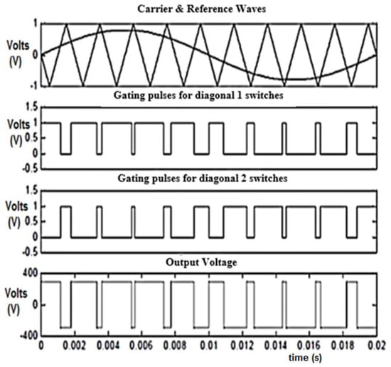
Figure 1.
Bipolar pulse width modulation (PWM).
2.5.2. Multi-Level Inverter
Multi-level inverters used to produce a low-distortion sine wave. They are used in applications that require a lot of electricity [23]. The waveform will appear to follow the sine wave as the output voltage level rises. As the amount is raised, the inverter’s power quality also increases. It also has some disadvantages. The number of components and switching losses increases as the amount rises. It has gate circuits as well.
The gate drive is a power amplifier that uses the controller I.C.’s low power input to produce high-current gate drives for power switches (MOSFETs, IGBTs, and so on). In certain situations, the PWM controller does not have enough output current to open and close the drive power supply’s capacitance. Gate drivers are often made up of transistors and transformers. Since integrated circuits have no distinct components, they are a good choice for gate drivers. As a result, the L293D integrated circuit was used in this project.
It is an integrated circuit powered by two H-bridge motors (I.C.). It performs the role of a current amplifier. It receives a low-current control signal at the input and drives the power switch with a high-current drive signal. The amplified current signal powers the motor. The pin diagram of the L293D I.C. is shown in Figure 2.
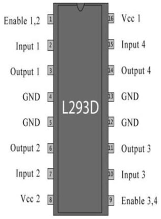
Figure 2.
Pin diagram of the L293D integrated circuit.
2.6. Filter Design
A filter is a system whose purpose is to attenuate the signal slightly in a particular group of frequencies (called the passband) and block the signal in a different group (called the stop band) [24]. A filter eliminates any additional frequency components above the predefined frequency to get a pure sine wave (cut-off frequency). Passive filters and active filters are the two types of filters. Passive filters consist only of passive components such as resistors, capacitors, and inductors. Integrated circuits, op-amps, transistors, or passive components (capacitors, resistors, and inductors) are combined in active filters.
The low-pass L.C. filter’s transfer function is as follows.
The cut-off frequency can be obtained in a few different ways.
The low and high harmonics are removed by setting the cut-off frequency as close to the 60 Hz fundamental frequency as possible.
2.7. Inverter Switching and Voltage Levels
Level and Polarity Generation
The switching table for the eight IGBTs used in the topology is included in this section [25]. This topology is made up of separate parts for generating the level and polarity. The level of the topology and polarity generation sections are shown in Figure 3.
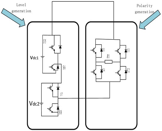
Figure 3.
Level and polarity generation.
Switches S1, S2, S3, and S4 are responsible for polarity generation, while switches S5, S6, S7, and S8 are responsible for output voltage levels. Since both Vdc1 and Vdc2 have different voltages, the topology is asymmetric.
Vdc1 is 72 volts, and Vdc2 is 144 volts. S1 and S2 only contribute when the output voltage is produced in the positive half cycle, while S3 and S4 contribute when the output voltage is generated in the negative half cycle. Below is a list of all switches and associated switching tables [26].
Table 1 depicts the flipping of the topology’s eight switches. Table 2 shows that S1 and S2 are ON during the positive half cycle, while S3 and S4 add to the voltage level during the negative half cycle. The circuit’s various operating levels are listed below.
Table 2.
Positive cycle operation of CHB MLI.
Table 2 depicts the flipping of the topology’s eight switches. It shows that S1 and S2 are ON during the positive half cycle, while S3 and S4 add to the voltage level during the negative half cycle. The circuit’s various operating modes are listed below.
Level 1: Switches 1, 2, 6, and 7 are activated in this mode. Vdc1 is the voltage that appears through the load. Figure 4 depicts the current direction.
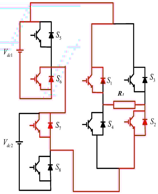
Figure 4.
Level 1 of operation.
Level 2: Switches 1, 2, 5, and 8 are activated in the second mode. Vdc2 appears to be the voltage around the load. Figure 5 depicts the direction of the current.
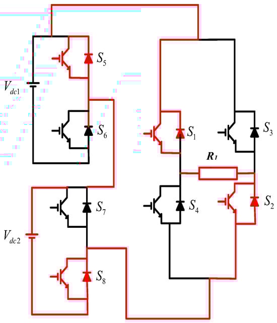
Figure 5.
Level 2 of operation.
Level 3: Switches 1, 2, 6, and 8 are activated in this mode. (Vdc1 + Vdc2) is the voltage that appears through the load. Figure 6 depicts the current course.
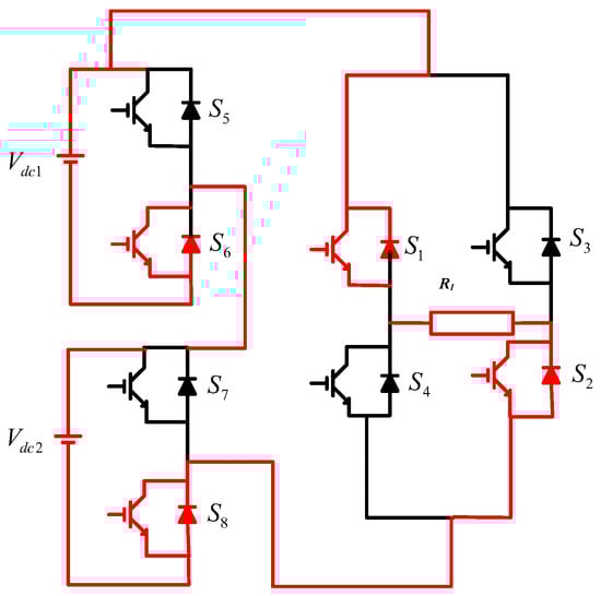
Figure 6.
Level 3 of operation.
The zero-cycle operation of CHB MLI values are given in Table 3. At the same time, the negative cycle operation of CHB MLI is shown in Table 4. Zero-cycle operation of CHB MLI are shown in Figure 7.
Table 3.
Zero-cycle operation of CHB MLI.
Table 4.
Negative cycle operation of CHB MLI.
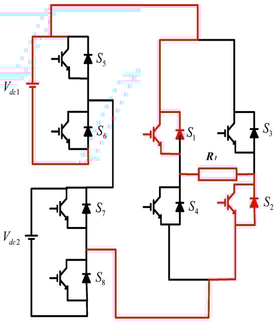
Figure 7.
Operation of zero level.
Level 5: Switches 3, 4, 6, and 7 are activated in this mode. The voltage across the load is -Vdc1, and the load current direction is shown in Figure 8.
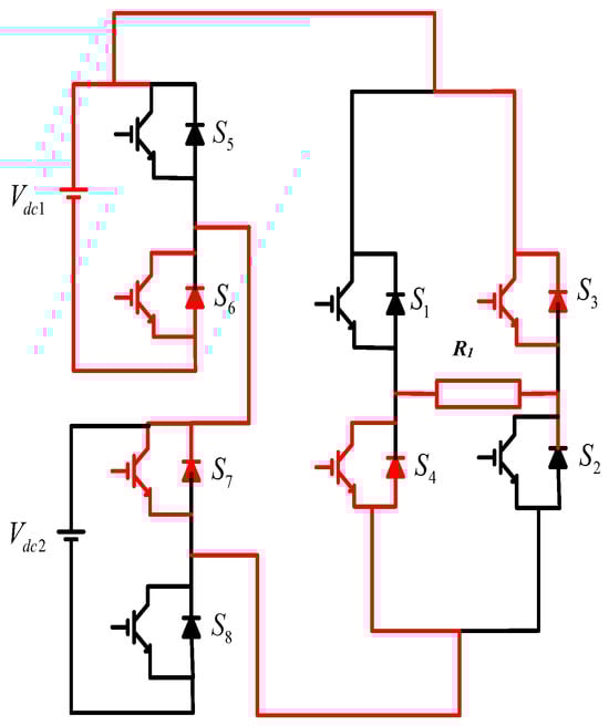
Figure 8.
Level of operation 5.
Level 6: Switches 3, 4, 5, and 8 are activated in this mode. The voltage across the load is -Vdc2, and the load current direction is shown in Figure 9.
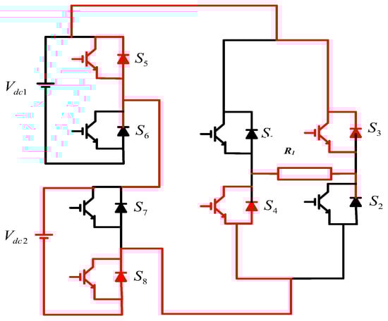
Figure 9.
Level of operation 6.
Level 7: Switches 3, 4, 6, and 8 are activated in this mode. −(Vdc1 + Vdc2) is the voltage that occurs through the load. Figure 10 depicts the current direction.
Figure 10.
Level of operation 7.
3. Sinusoidal Pulse Width Modulation (SPWM) for Multi-Level Inverter (MLI)
The traditional SPWM modulation technology generates PWM waveforms by comparing triangular carrier waves with sinusoidal modulation waves, while the multi-carrier SPWM modulation technology is based on multi-carrier sinusoidal pulse width modulation [27]. The principle of multi-carrier SPWM modulation technology is to use multiple triangular carrier signals and the same sinusoidal reference signals to generate switching signals by comparing them. The multi-carrier SPWM technology is one of the most common modulation methods for multi-level inverters. It is a direct extension of the two-stage SPWM technology used in multi-level inverters. There are two kinds of standard multi-carrier SPWM modulation techniques: SPWM based on carrier vertical phase shift and SPWM based on carrier horizontal phase shift. The modulation strategy of POD and APOD belongs to the carrier vertical phase shifting SPWM modulation strategy. Its basic principle is as follows: if the output voltage level of the inverter is n, n − 1 triangular carriers with the same frequency and phase are needed. These N − 1 carriers are placed side by side to form a carrier group, and the horizontal center line of the group is taken as the actual reference line; the carrier groups are symmetrically distributed below the reference zero line and modulated by the same sinusoidal modulation wave to obtain the corresponding switching pulse control signal.
- POD (phase opposition disposition)
The carrier signals above and below the reference/zero line are in phase. However, they become 180 degrees out of phase below and above the zero line. At the output side of the CHB multi-level inverter, the necessary output voltage waveform is obtained using the POD multi-carrier PWM technique [28].
- APOD (alternate phase opposition disposition)
Any carrier wave shape in APOD modulation is 180 degrees out of phase with its adjacent carrier. Since the APOD and POD systems are the same with three-level inverters, a seven-level inverter addresses the APOD system [29].
- Harmonic analysis of APOD and POD modulation strategies
According to the theory of bilateral Fourier transform, the harmonic expression of the output waveform of any PWM modulation technology based on carrier wave can be expressed as follows:
where, , , is the base frequency, is the carrier frequency, and the factor is .
Factor B is as follows:
Because y = ω0t, x = ωct, the harmonic form of the voltage contained in formula n can be expressed as , and there are three cases:
- When is a fundamental or harmonic wave.
- When is the carrier’s harmonic and the carrier’s multiplier.
- When is a carrier multiple of the side-band harmonics.
For the inverters with the N output level, the carrier vertical phase shifting SPWM modulation strategy requires N − 1 carrier, N’ = (N − 1)/2 carriers in positive and negative half-circles, 1 peak of the triangular carrier, 1 modulation wave, modulation degree, and the smallest integer greater than N’ M to be set. According to the above bilateral Fourier transformation theory, the harmonic analysis expression for APOD is as follows:
where, , , , is
When , the harmonic resolution expression of APOD is as follows:
where is
The formula shows that when working at [N’M] N, the output voltage of the inverter does not have carrier harmonics and carrier multiples, only side-band harmonics of carrier multiples [30]. When working at [N’M] > N, the harmonic content increases the odd times of the base wave, while the other harmonic content is the same as the linear modulation region; only the amplitude is different. It is also known from the formula that the equivalent frequency does not increase with the increase in N but remains fc; the output harmonic amplitude decreases with the rise in the number of levels.
POD modulation strategy output voltage harmonic expression is as follows:
When
When
From these formulas, it can be seen that the harmonic characteristics of the POD modulation voltage are the same as that of the APOD modulation output when working at . When working in , the odd harmonic of the base wave is increased. The equivalent carrier frequency is still fc and has not been improved [31].
4. Results and Discussions
4.1. Simulation Model
A multi-level inverter simulation was successfully built using MATLAB 2017b and eight IGBT switches were used in the MLI—the 72 V and 144 V input D.C. voltage sources, respectively. The remaining four IGBT switches are connected to the R.L. load side, which acts as a polarity generator in the MLI, and the remaining four IGBT switches are connected to a D.C. voltage source, which serves as a voltage level generator. To obtain the necessary output voltage level at the multi-level inverter’s output, PWM techniques are used: phase opposition disposition (POD), alternative phase opposition disposition (APOD), and PWM with multiple carriers. A voltage waveform with seven levels is produced via multi-carrier PWM. The FFT tool in MATLAB 2017b can be used to calculate the total harmonic distortion (THD). The logical circuit side of the simulation model’s OR, XOR, NXOR, and NOT gates regulate the switching operation (ON and OFF) in the CHB MLI, as illustrated in Figure 11. The specification of the parameters is given in Table 5.
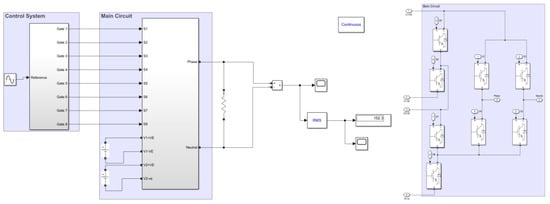
Figure 11.
Simulation model of CHB-MLI.
Table 5.
The specification of the parameters used in the simulation model.
For the control circuit, seven repeating sequences are used and compared with the sinusoidal waveform; it can be seen and analyzed with the help of scope that seven relational operators are used, which connect with the seven repeating sequences and logical gates (XOR and NXOR); the logical gates are sent signal through switching gates, which turn the IGBT in MLI ON and OFF to obtain the seven-level output voltage waveform at the export of CHB-MLI. The Control Circuit of Simulation Model is shown in Figure 12.
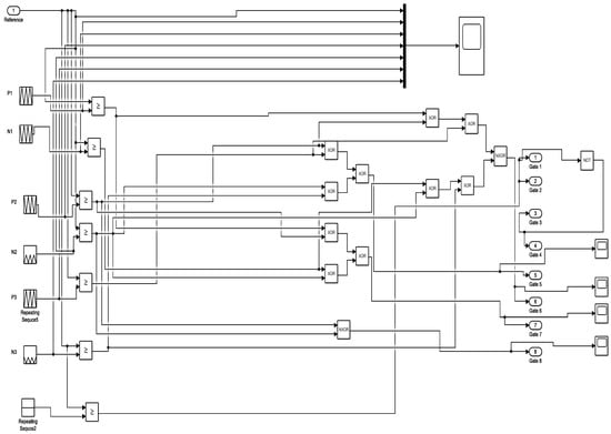
Figure 12.
Control Circuit of Simulation Model.
4.2. Simulation Results
In this section, we present the simulation results. After obtaining the harmonic analytical expression of the above multi-level modulation strategy, taking APOD and POD modulation strategy as an example, MATLAB was used for simulation to verify the harmonic characteristics indicated by the analytical expression.
4.2.1. APOD MC PWM Modulation Strategy
In this section, we present the simulation of the inverter of the APOD modulation strategy. The diagram of the simulation is shown in Figure 11. When the high voltage D.C. bus voltage is set at 144 V and the low voltage D.C. bus voltage is set at 72 V, then the output voltage levels are 216 V, 144 V, 72 V, 0 V, −72 V, −144 V, −216 V.
The APOD modulation strategy was adopted for the inverter modulation strategy, and the carrier frequency was set at 1 kHz, 5 kHz, and 10 kHz, respectively. The carrier and modulation waveforms with the carrier frequency set at 1 kHz are shown in Figure 13; the voltage simulation waveform with the carrier frequency set at 1 kHz is shown in Figure 14; and the THD analysis with the carrier frequency set at 1 kHz is shown in Figure 15.
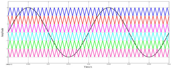
Figure 13.
Carrier and modulation of APOD MC PWM waveform with 1 kHz frequency.
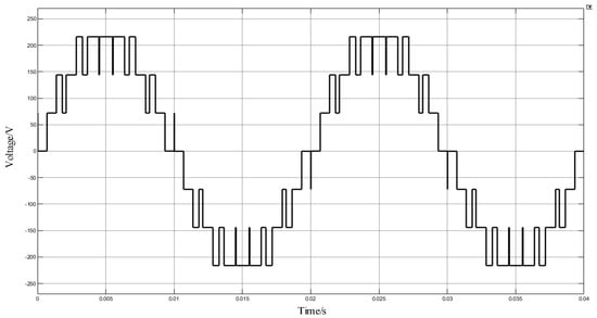
Figure 14.
Voltage waveform of APOD MC PWM with 1 kHz frequency.

Figure 15.
Total harmonic distortion of APOD MC PWM with 1 kHz frequency.
The carrier and modulation waveforms with the carrier frequency set at 5 kHz are shown in Figure 16; the voltage simulation waveform with the carrier frequency set at 5 kHz is shown in Figure 17; and the THD analysis with the carrier frequency set at 5 kHz is shown in Figure 18.
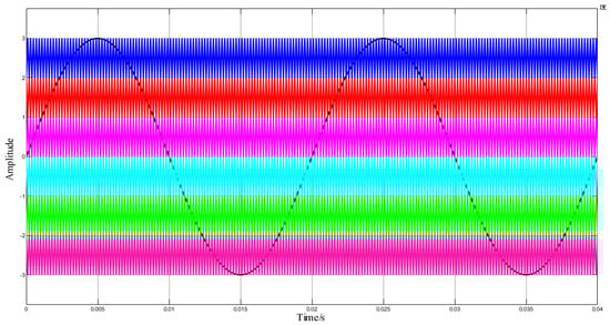
Figure 16.
Carrier and modulation of APOD MC PWM waveform with 5 kHz frequency.

Figure 17.
Voltage waveform of APOD MC PWM with 5 kHz frequency.
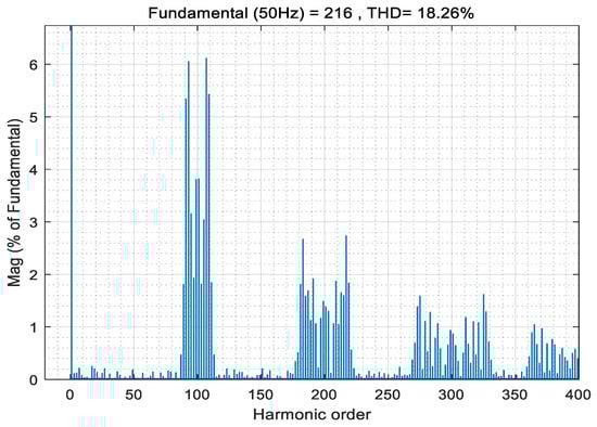
Figure 18.
Total harmonic distortion of APOD MC PWM with 5 kHz frequency.
The carrier and modulation wave waveforms with the carrier frequency set at 10 kHz are shown in Figure 19; the voltage simulation waveform with the carrier frequency set at 10 kHz is shown in Figure 20; and the THD analysis with the carrier frequency set at 10 kHz is shown in Figure 21.
Figure 19.
Carrier and modulation of APOD MC PWM waveform with 10 kHz frequency.
Figure 20.
Voltage waveform of APOD MC PWM with 10 kHz frequency.
Figure 21.
Total harmonic distortion of APOD MC PWM with 10 kHz frequency.
It can be seen from Figure 15, Figure 18 and Figure 21 that the most severe harmonic caused by the APOD modulation strategy is located at the primary carrier frequency fc, and more harmonic energy is injected into the carrier harmonic. There are carrier harmonics and carrier multiple side-band harmonics in the spectrum, and the average switching frequency of the switch device is equal to the carrier frequency. This is relevant to the theoretical analysis results of Formulas (10) and (11). At the same time, from the simulation results, simply changing the modulation frequency has little effect on the THD.
4.2.2. POD MC PWM Modulation Strategy
The POD modulation strategy was adopted for the inverter modulation strategy, and the carrier frequency was set at 1 kHz, 5 kHz, and 10 kHz, respectively. The carrier and modulation waveforms with the carrier frequency set at 1 kHz are shown in Figure 22; the voltage simulation waveform with the carrier frequency set at 1 kHz is shown in Figure 23; and the THD analysis with the carrier frequency set at 1 kHz is shown in Figure 24.
Figure 22.
Carrier and modulation waveform of POD MC PWM with 1 kHz frequency.
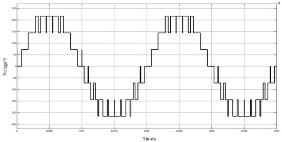
Figure 23.
Voltage waveform of POD MC PWM with 1 kHz frequency.
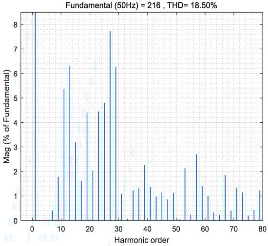
Figure 24.
Total harmonic distortion of POD MC PWM with 1 kHz frequency.
The carrier and modulation wave waveforms with the carrier frequency set at 5 kHz are shown in Figure 25; the voltage simulation waveform with the carrier frequency set at 5 kHz is shown in Figure 26; and the THD analysis with the carrier frequency set at 5 kHz is shown in Figure 27.
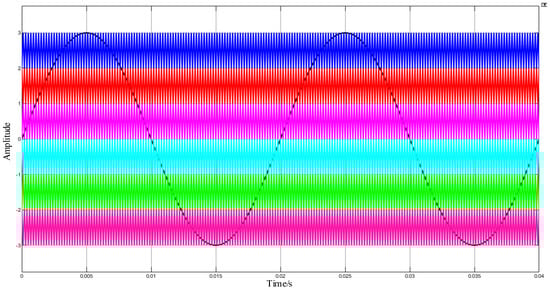
Figure 25.
Carrier and modulation waveform of POD MC PWM with 5 kHz frequency.
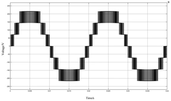
Figure 26.
Voltage waveform of POD MC PWM with 5 kHz frequency.
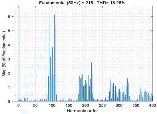
Figure 27.
Total harmonic distortion of POD MC PWM with 5 kHz frequency.
The carrier and modulation waveforms with the carrier frequency set at 10 kHz are shown in Figure 28; the voltage simulation waveform with the carrier frequency set at 10 kHz is shown in Figure 29; and the THD analysis with the carrier frequency set at 10 kHz is shown in Figure 30.
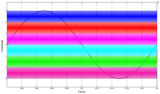
Figure 28.
Carrier and modulation waveform of POD MC PWM with 10 kHz frequency.

Figure 29.
Voltage waveform of POD MC PWM with 10 kHz frequency.
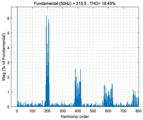
Figure 30.
Total Harmonic Distortion of POD MC PWM with 10 kHz frequency.
It can be seen from Figure 24, Figure 27 and Figure 30 that the most severe harmonic caused by the POD modulation strategy is located at the primary carrier frequency fc, and more harmonic energy is injected into the carrier harmonic. There are carrier harmonics and carrier multiple side-band harmonics in the spectrum, and the average switching frequency of the switch device is equal to the carrier frequency. This is relevant to the theoretical analysis results of Formulas (10) and (11). At the same time, from the simulation results, simply changing the modulation frequency has little effect on the THD.
4.2.3. Variable Carrier Frequency APOD Modulation Strategy
The variable carrier frequency SPWM modulation strategy can improve the equivalent carrier frequency, and the APOD modulation strategy can efficiently decrease the harmonic content of the output voltage. By combining the two, this paper proposes a variable carrier frequency APOD modulation strategy (VF-APOD).
The schematic diagram of the simulation structure is shown in Figure 11. When the high voltage D.C. bus voltage is set at 144 V and the low voltage D.C. bus voltage is set at 72 V, then the output voltage levels are 216 V, 144 V, 72 V, 0 V, −72 V, −144 V, −216 V. The variable carrier frequency VF-APOD modulation strategy is used in the inverter. The carrier frequencies are 1 kHz, 4 kHz, and 500 Hz, respectively. The carrier and modulation waveforms are shown in Figure 31; the voltage simulation waveform is shown in Figure 32; and the THD analysis is shown in Figure 33.
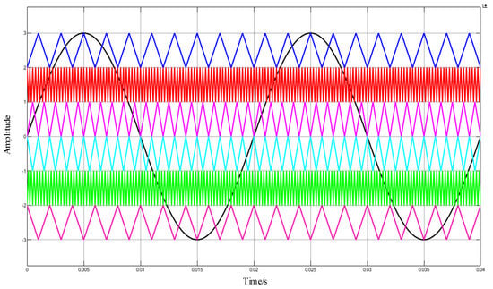
Figure 31.
Carrier and modulation waveform of VF-APOD MC PWM.
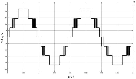
Figure 32.
Voltage simulation waveform of VF-APOD MC PWM.
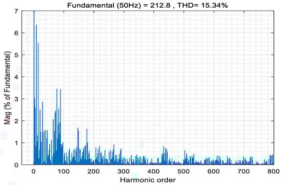
Figure 33.
Total Harmonic Distortion of VF-APOD MC PWM.
The simulation results show that the THD decreased significantly, from 18% to 15.34%. At the same time, compared with the APOD modulation strategy, the switching frequency of the VF-POD modulation strategy is much lower. Theoretically, this modulation strategy can significantly reduce the switch’s loss and performance requirements.
4.3. DSP Programming
The experiment platform uses the In TI DSP 28335 as the controller; the control strategy is programmed in C language; and the control platform is shown in Figure 34. The C code of the control strategy is shown in Figure 35.
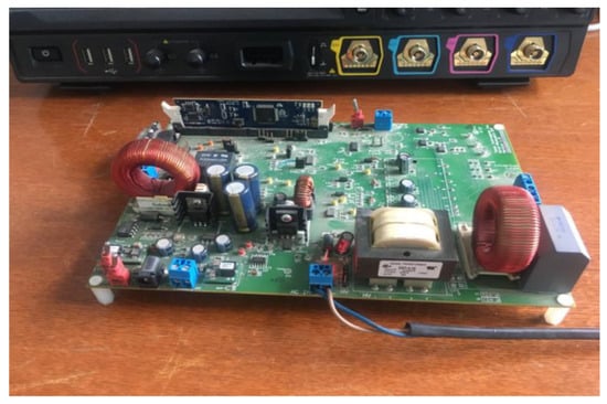
Figure 34.
DSP control platform.

Figure 35.
Code of DSP programming.
4.4. Real-Time Simulation Testing in Xsim System
To test the control function, the primary seven-level converter model is built up in the Xsim real-time simulation system. The Xsim system provides a rapid development platform from simulation to prototype and realizes the application of the simulation model in product development, simulation verification, and closed-loop testing. By adopting parallel computing and simulation technology, the Xsim system recognizes the functions of real-time simulation.
The simulation monitoring software is shown in Figure 36. The simulation model can be compiled, the code can be automatically generated and downloaded, the simulation process can be monitored, the results can be displayed, and the parameters can be adjusted online. The parallel computation of the simulation model and real-time storage of simulation data are realized. In addition, the real-time simulator with the I.O. interface board card is used to complete the analog and digital signal high-speed acquisition and output, as well as the real-time simulator and other equipment clock synchronization and data communication.
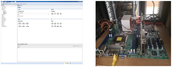
Figure 36.
Real-time hardware and software simulations of the Xsim system.
The carrier waveform and modulation based on APOD from the Xsim system are shown in Figure 37. The output voltage of the inverter from the Xsim system is shown in Figure 38.
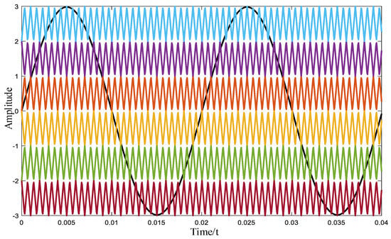
Figure 37.
Carrier and modulation waveform from the Xsim system.
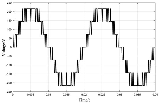
Figure 38.
Waveform of output voltage from the Xsim system.
In the above discussion, the correctness of the theoretical analysis of the APOD and POD modulation strategy is verified by the simulation of a multi-level converter at different frequencies, and a VF-APOD modulation strategy is proposed and simulated based on it, which verifies the advantage of the variable carrier VF-APOD in reducing the THD.
5. Conclusions
MATLAB successfully implemented the multi-level inverter model to generate a seven-level output voltage waveform for the CHB MLI. Two modulation techniques, APOD (alternate phase opposition disposition) MC PWM and POD (phase opposition disposition) MC PWM, were used to obtain the desired output voltage waveform. The THD (total harmonic distortion) was determined and analyzed using the FFT tool in MATLAB. The APOD technique achieved an output voltage THD of 18.27%, while the APOD PWM technique achieved an output current THD of 15.67%. On the other hand, the POD PWM technique achieved an output voltage THD of 18.06% and an output current THD of 15.45%. The results have established that the POD multi-carrier PWM produces more precise output voltage and current waveforms compared to the APOD multi-carrier pulse width modulation (PWM).
Author Contributions
Conceptualization, K.B., G.A. and P.M.; Methodology, G.A. and M.H.; Software, K.B. and A.E.; Validation, E.T.; Investigation, E.T. and A.E.; Writing—original draft, K.B. and G.A.; Writing—review & editing, K.B., M.H., E.T., A.E. and P.M.; Visualization, M.H.; Supervision, P.M., Funding acquisition, A.E. All authors have read and agreed to the published version of the manuscript.
Funding
This research was funded by Northern Border University, Arar, Saudi Arabia.
Data Availability Statement
The data presented in this study are available on request from the corresponding author.
Acknowledgments
The authors extend their appreciation to the Deanship of Scientific Research at Northern Border University, Arar, KSA for funding this research work through the project number “NBU-FPEJ-2024-2448-01”.
Conflicts of Interest
The authors declare no conflicts of interest.
References
- Wang, L.; Han, X.; Gao, Y. Research of Construction and Practice of Blended “Golden Course” Teaching Based on C language programming. In Proceedings of the 2021 2nd International Conference on Big Data and Informatization Education (ICBDIE), Hangzhou, China, 2–4 April 2021; pp. 587–590. [Google Scholar] [CrossRef]
- Xiao, M.; Xu, Q.; Ouyang, H. An Improved Modulation Strategy Combining Phase Shifted PWM and Phase Disposition PWM for Cascaded H-Bridge Inverters. Energies 2017, 10, 1327. [Google Scholar] [CrossRef]
- Sekar, R.M.; Murugesan, S.; Devadasu, G.; Salkuti, S.R. A Coyote Optimization-Based Residual Attention Echo State Reactive Controller for Improving Power Quality in Grid-PV Systems. Machines 2023, 11, 384. [Google Scholar] [CrossRef]
- Krishnamoorthy, U.; Pitchaikani, U.; Rusu, E.; Fayek, H.H. Performance Analysis of Harmonic-Reduced Modified PUC Multi-Level Inverter Based on an MPC Algorithm. Inventions 2023, 8, 90. [Google Scholar] [CrossRef]
- Babkrani, Y.; Naddami, A.; Hayani, S.; Hilal, M.; Fahli, A. Simulation of Cascaded H—Bridge Multilevel Inverter with Several Multi-carrier Waveforms and Implemented with P.D., POD and APOD Techniques. In Proceedings of the 2017 International Renewable and Sustainable Energy Conference (IRSEC), Tangier, Morocco, 4–7 December 2017; pp. 1–6. [Google Scholar] [CrossRef]
- Noman, A.M.; Al-Shamma’a, A.A.; Addoweesh, K.E.; Alabduljabbar, A.A.; Alolah, A.I. Cascaded Multilevel Inverter Topology Based on Cascaded H-Bridge Multilevel Inverter. Energies 2018, 11, 895. [Google Scholar] [CrossRef]
- Noorsal, E.; Rongi, A.; Ibrahim, I.R.; Darus, R.; Kho, D.; Setumin, S. Design of FPGA-Based SHE and SPWM Digital Switching Controllers for 21-Level Cascaded H-Bridge Multilevel Inverter Model. Micromachines 2022, 13, 179. [Google Scholar] [CrossRef] [PubMed]
- Balamurugan, S.; Palanisamy, R.; Karthikeyan, B. Experimental Investigation of Modular Multilevel Converter Using Space Vector Pulse Width Modulation. J. Electr. Eng. Technol. 2023. [Google Scholar] [CrossRef]
- Soltani, M.; Pairo, H.; Shoulaie, A. Modelling approach for multi-carrier-based pulse-width modulation techniques utilised in asymmetrical cascaded H-bridge inverters. IET Power Electron. 2019, 12, 3822–3832. [Google Scholar] [CrossRef]
- Mahmoud, M.M.; Atia, B.S.; Esmail, Y.M.; Ardjoun, S.A.E.M.; Anwer, N.; Omar, A.I.; Alsaif, F.; Alsulamy, S.; Mohamed, S.A. Application of Whale Optimization Algorithm Based FOPI Controllers for STATCOM and UPQC to Mitigate Harmonics and Voltage Instability in Modern Distribution Power Grids. Axioms 2023, 12, 420. [Google Scholar] [CrossRef]
- Rao, B.N.; Suresh, Y.; Naik, B.S.; Venkataramanaiah, J.; Aditya, K.; Panda, A.K. A novel single source multilevel inverter with hybrid switching technique. Int. J. Circuit Theory Appl. 2022, 50, 794–811. [Google Scholar] [CrossRef]
- Garcia-Reyes, L.A.; Beltrán-Telles, A.; Bañuelos-Ruedas, F.; Reta-Hernández, M.; Ramírez-Arredondo, J.M.; Silva-Casarín, R. Level-Shift PWM Control of a Single-Phase Full H-Bridge Inverter for Grid Interconnection, Applied to Ocean Current Power Generation. Energies 2022, 15, 1644. [Google Scholar] [CrossRef]
- Memon, R.; Mahar, M.A.; Larik, A.S.; Shah, S.A.A. Design and Performance Analysis of New Multilevel Inverter for PV System. Sustainability 2023, 15, 10629. [Google Scholar] [CrossRef]
- Khasim, S.R.; Dhanamjayulu, C. Design and Implementation of Asymmetrical Multilevel Inverter with Reduced Components and Low Voltage Stress. IEEE Access 2022, 10, 3495–3511. [Google Scholar] [CrossRef]
- Wang, Z.; He, Z.; Gao, C. A Systematic Study on the Harmonic Overlap Effects for DC/AC Converters under Low Switching Frequency Modulation. Energies 2021, 14, 2811. [Google Scholar] [CrossRef]
- Prasad, D.; Dhanamjayulu, C. Reduced Voltage Stress Asymmetrical Multilevel Inverter with Optimal Components. IEEE Access 2022, 10, 53546–53559. [Google Scholar] [CrossRef]
- Almakhles, D.; Jayachandran, D.N.; Anbazhagan, L.; Hannachi, M.; Mohamed Ali, J.S. Dynamic Analysis of Extendable Hybrid Voltage Lift DC–DC Converter for DC Microgrid. Processes 2022, 10, 2652. [Google Scholar] [CrossRef]
- Mohammed, M.F.; Qasim, M.A. Single Phase T-Type Multilevel Inverters for Renewable Energy Systems, Topology, Modulation, and Control Techniques: A Review. Energies 2022, 15, 8720. [Google Scholar] [CrossRef]
- Lin, B.-R.; Liu, Y.-C. Analysis of a Wide Voltage Hybrid Soft Switching Converter. Electronics 2021, 10, 473. [Google Scholar] [CrossRef]
- Odeh, C.I.; Kondratenko, D.; Lewicki, A.; Morawiec, M.; Jąderko, A.; Baran, J. Pulse-Width Modulation Template for Five-Level Switch-Clamped H-Bridge-Based Cascaded Multilevel Inverter. Energies 2021, 14, 7726. [Google Scholar] [CrossRef]
- Smadi, I.A.; Albatran, S.; Alsyouf, M.A. Optimal Control of a Compact Converter in an AC Microgrid. Electronics 2018, 7, 102. [Google Scholar] [CrossRef]
- Zhao, L.; Xu, C.; Zheng, X.; Li, H. A Dual Half-Bridge Converter with Adaptive Energy Storage to Achieve ZVS over Full Range of Operation Conditions. Energies 2017, 10, 444. [Google Scholar] [CrossRef]
- Habib, S.; Abbas, G.; Jumani, T.A.; Bhutto, A.A.; Mirsaeidi, S.; Ahmed, E.M. Improved Whale Optimization Algorithm for Transient Response, Robustness, and Stability Enhancement of an Automatic Voltage Regulator System. Energies 2022, 15, 14. [Google Scholar] [CrossRef]
- Das, B.; Bhattacharya, A.; Chatterjee, D.; Kasari, P.R. Development of modified cascaded multilevel inverter configuration with less number of switches. In Proceedings of the TENCON 2017—2017 IEEE Region 10 Conference, Penang, Malaysia, 5–8 November 2017; pp. 1550–1555. [Google Scholar] [CrossRef]
- Rawa, M.; Mohamed Ali, J.S.; Siddique, M.D.; Mekhilef, S.; Wahyudie, A.; Seyedmahmoudian, M.; Stojcevski, A. A New Multilevel Inverter Topology with Reduced DC Sources. Energies 2021, 14, 4709. [Google Scholar] [CrossRef]
- Wang, H.; Yang, G.; Kang, W.; Zhang, X.; Fan, X.; Xiao, F. Minimum-Output-Current-Ripple Control of Current-Fed Three-Level Phase-Shift Full-Bridge Converter. Energies 2022, 15, 6444. [Google Scholar] [CrossRef]
- Ch, L.R. Analysis of THD for Multilevel Inverters with Novel Pulse Width Modulation Techniques. In Proceedings of the 2021 IEEE International Conference on Intelligent Systems, Smart and Green Technologies (ICISSGT), Visakhapatnam, India, 13–14 November 2021; pp. 150–155. [Google Scholar] [CrossRef]
- Paramasivan, M.; Eswaramoorthy, K.; Muniraj, R.; Kanthan, P.L.; Babu, T.S.; Jeevananthan, S.; Alhelou, H.H. An Alternative Level Enhanced Switching Angle Modulation Schemes for Cascaded H Bridge Multilevel Inverters. IEEE Access 2023, 11, 57365–57382. [Google Scholar] [CrossRef]
- Aljafari, B.; Rameshkumar, K.; Indragandhi, V.; Ramachandran, S. A Novel Single-Phase Shunt Active Power Filter with a Cost Function Based Model Predictive Current Control Technique. Energies 2022, 15, 4531. [Google Scholar] [CrossRef]
- Sunddararaj, S.P.; Srinivasarangan Rangarajan, S. An Extensive Review of Multilevel Inverters Based on Their Multifaceted Structural Configuration, Triggering Methods and Applications. Electronics 2020, 9, 433. [Google Scholar] [CrossRef]
- Siddique, M.D.; Mekhilef, S.; Shah, N.M.; Ali, J.S.M.; Meraj, M.; Iqbal, A.; Al-Hitmi, M.A. A New Single Phase Single Switched-Capacitor Based Nine-Level Boost Inverter Topology With Reduced Switch Count and Voltage Stress. IEEE Access 2019, 7, 174178–174188. [Google Scholar] [CrossRef]
Disclaimer/Publisher’s Note: The statements, opinions and data contained in all publications are solely those of the individual author(s) and contributor(s) and not of MDPI and/or the editor(s). MDPI and/or the editor(s) disclaim responsibility for any injury to people or property resulting from any ideas, methods, instructions or products referred to in the content. |
© 2024 by the authors. Licensee MDPI, Basel, Switzerland. This article is an open access article distributed under the terms and conditions of the Creative Commons Attribution (CC BY) license (https://creativecommons.org/licenses/by/4.0/).