1. Introduction
It is well known that processes involving metallic and semiconductor nanoparticles are at the base of many phenomena of both academic and practical interest. Their understanding is required for the investigation and utilization of conduction, sensor, photoelectric, catalytic, magnetic and other properties of nanocomposite materials [
1,
2,
3,
4,
5,
6,
7,
8,
9]. It is clear that any investigation into the processes occurring in nanoparticles must focus on their charge structure.
The distribution of conduction electrons along the particle radius may be considered, due to their very high density, uniform for metallic nanoparticles. For semiconductor nanoparticles, however, the situation is drastically different. One should distinguish between semiconductor nanoparticles with low cm and high – cm conduction electron densities. In both cases, the density is quite strongly temperature dependent.
Semiconductors with low conduction electron densities have less than one electron in the nanoparticle of the radius
R = 50 nm (nanoparticles of
and
may serve as such an examples). It makes no sense, therefore, to speak about the electron structure of the nanoparticle in this case. In the case of the high conduction electron density (for example,
nanoparticles), the particle of the same size contains from
to
electrons [
10,
11]. It is then possible, with good reason, to consider the concept of the charge or electronic structure of a nanoparticle. At such numbers, electrons form a definitive distribution along the radius, with part of them being pushed to the surface where they form a negatively charged surface layer (see, for example, [
12,
13]).
The choice of
nanoparticles as the object of study is due to several reasons. As is well known, nanostructured indium is widely used in microelectronics in the production of solar cells and phosphors, as well as high-temperature thermoelectric material [
14]. The possibility of using indium in these areas is largely determined by the high concentration of conduction electrons, and especially by its concentration in the near-surface region of nanoparticles. Therefore, the elucidation of the distribution of electrons over the volume of nanoparticles is an extremely important task. Note also that a comparison of the theory with experimental data proposed in this article will be carried out for the sensor effect, for which the near-surface electron concentration is the determining factor.
The calculation of the electron distribution along the radius reduces to the problem of finding a minimum of the free energy (F). From the mathematical point of view, this is a problem of calculus of variations. Furthermore, conservation laws dictate some additional restrictions that must be imposed. Specifics of the functionals (F), considered in the present paper, are their rather complicated form. For this reason, the application of the theory developed in the present study to the functionals of the type (F) is a non-trivial task. The calculation of the variation of the functional is presented in a separate appendix of the paper. Conservation restrictions, upon the calculation of the variation, are being taken into account directly, without involving Lagrange multipliers. While canonical functionals give rise to a differential equation for the extremal, the corresponding equation in the present case is formally a nonlinear integro-differential.
This paper provides a detailed iterative solution process of the equation for the extremal. In order for discussion to be easily understandable, it is illustrated using the problem of calculation of a sensor effect. Sensors are devices that allows the detection of various substances, in particular gases, in different media. An example of such an application is a detection in the atmosphere of substances carrying fire and explosion hazards, as well as other gases having adverse effects on human health. The sensor effect manifests itself as a change in the conductance of the sensitive layer of a detector upon the action of gases that are being traced. As shown in the investigations [
15,
16], the conductance of a nano-structured sensitive layer depends on the electron distribution within the nanoparticle. The sensitivity of the detector is defined as a ratio of film conductance in the presence of hydrogen with the pressure
to conductance in its absence. This corresponds to the ratio of respective near-surface densities of conduction electrons in nanoparticles
, where
R is the nanoparticle radius.
There is a significant number of studies devoted to the mechanism of the sensor effect; their detailed discussion is available in the review [
17]. Equally, there are many studies discussing relevant calculation methodologies, for example, [
18,
19]. These papers consider the solution of Poisson’s equation for spherical nanocrystal of a variable radius only. They consider neither the set of kinetic equations on the surface of the nanoparticle or the problem of minimization of free energy in the presence of restrictions. It is also worth while to mention the studies [
15,
20], which do consider, in some form, such formulations, but with a major emphasis on physics. Related essential techniques of the computational mathematics are not discussed in sufficient detail in these papers. The present paper aims at comprehensive discussion of mathematical problems, related to quantification of the sensor effect, such as minimization of free energy (i.e., calculation of variation), description of processes in negatively charged surface layer, and consideration of more complicated kinetics.
The present paper uses the following approach. The set of kinetic equations, describing various physico-chemical processes occurring on the surface of nanoparticle, is being developed. The solution of this set of equations determines the density of surface charges uniquely. Further, this set of equations is solved together with the problem of minimization of free energy. The solution of the set of kinetic equations, corresponding to the processes on the surface of the nanoparticle, provides the boundary condition for the Poisson’s equation.
2. Mathematical Formulation
The formalisation of the problem under consideration is reduced to the solution of two mathematical problems. The first is the location of stationary points of the set of kinetic equations describing the physico-chemical processes on the surface of the nanoparticle of a given material, for example, .
The chemical processes that take place on the surface of a nanoparticle are complicated and multistep, consisting of a large number of reactions. Let us consider only the most important reactions that take place on the surface of an indium oxide nanoparticle in the atmosphere:
Reaction (I) corresponds to the adsorption and desorption of molecular oxygen on the surface of a nanoparticle. Reaction (II) describes the dissociation of oxygen to atomic forms, as well as the reverse process. Reaction (III) corresponds to a conduction electron captured by an adsorbed atom of oxygen, and to the process of an electron returning to the volume of the nanoparticle [
21]. Reaction (IV) describes the recombination of neutral and charged atoms of oxygen. The key role in the calculation of the sensor effect belongs to reaction (V). Here, as a result of the reaction between gaseous hydrogen and adsorbed oxygen ions, a molecule of water is formed, while the released electron migrates to the interior of the particle, thus increasing electron conductance. This change of electron conductance in the presence of hydrogen, compared to its value in the absence of hydrogen, is known as a sensor effect. The following set of kinetic equations represents the chemical reactions (I)–(V):
In the following analysis, the steady-state form of the set of Equation (
1) is considered, since the sensor response time is much longer than the time constants of chemical reactions (I)–(V). Therefore, over the time comparable with the time constants, Equation (
1) reaches the equilibrium. The reaction rate constants are considered as known functions of temperature (see
Section 4). The unknowns are the surface density of the oxygen molecules
, the total surface density of all adsorbed forms of oxygen atoms (both neutral and negatively charged,
O and
)
, and the surface density
of negative ions
All of these variables have dimension [cm
. The set of Equation (
1) corresponds to the reaction scheme (I)–(V) and satisfies the laws of both the chemical kinetics and the theory of adsorption [
22,
23]. Various negatively charged forms of oxygen may adsorb on the surface of the nanoparticle. In the range of sensor work temperatures (
200–400 °C)
is the major form of adsorbed oxygen [
24].
The set of Equation (
1) is solved easily using, for example, the computational package Wolfram Mathematica. Note that the calculation of sensitivity to hydrogen requires the set of Equation (
1) to be solved twice (see flowchart), the first time in the absence of hydrogen
, and the second time with its presence
.
For a different nanostructured system, for example, with a large family of different nanoparticles, this system will be of much higher order, and inevitably more complicated. It may have multiple solutions, including complex ones. In any case, though, this will be the set of nonlinear algebraic equations. Since
includes densities of both the neutral and the charged O atoms, the solution satisfying the condition
must be singled out. In the case of an increased order, this set of steady-state equations is replaced by the set of nonsteady differential equations of chemical kinetics. Equilibrium points of the latter are solutions of the set of steady-state equations. Therefore, in the limit
, the solution of set of the nonsteady equations approaches the required steady-state solution. It is known [
25] that for the set of differential equations of chemical kinetics (in gaseous phase), the solution remains positive at any point in time if initial densities are non-negative. In particular, all the densities are positive at the equilibrium point. Moreover, such an equilibrium point is unique. As soon as the value
is found, the total charge on the nanoparticle’s surface
(used at the second step of solution) may be determined, along with the value
.
The following is the algorithm flowchart.

The second stage of the solution is much more demanding computationally. Here, it is necessary to find the electron density
and the density of positive ions
inside the nanoparticle, which provide the free energy minimum. At the same time, the balance between the total numbers of positive and negative charges
and
must be carried out. Negative oxygen atoms, located on the surface of nanoparticles, have also to be taken into account. All the variables
are dimensionless, i.e., just real numbers. From a mathematical point of view, this is the problem of calculus of variations with additional restriction [
26].
Let us present free energy of the nanoparticle as a sum of free energies of the interacting charges [
15,
27,
28].
Here
is the free energy of conduction electrons [
27]
where density of free energy
and
Here,
is the chemical potential,
is the effective mass of the electron, and
is the distribution of electron density over the radius inside of nanoparticles [
27]. The Formula (
4), as well as all subsequent formulae, are written in atomic units [
29].
Let us write down the potential energy of the interaction between positive and negative charges of the nanoparticle [
28].
where
is the binding energy of electrons on donors [
30] and
is the donor density within nanoparticles.
Free energy of positively charged donors has the form [
28]
where
is electrostatic potential within a semiconductor nanoparticle,
is the relative dielectric permittivity, and the function
satisfied the relationship
Formally, this relationship is not an equation since its left-hand side depends on the unknown function
, while the right-hand side depends on the unknown functions
and
.
The last term in the expression (
2) represents the free energy of negatively charged adsorbed ions of oxygen [
15]:
Here
is the binding energy of an electron with the adsorbed atom of oxygen.
It is necessary to find the functions
and
, which provide the minimum of free energy
F. For this purpose, it is necessary to calculate the variation of the functional (
2). Equating the variation to zero, we obtain relations that will be satisfied along the extremals (see
Appendix A)
is an arbitrary constant.
It follows from (
10) that
and
on the extremals are functions of
, and the electron density
is also a function of
Here, the polylogarithm special function
is defined as an infinite power
. The Wolfram Mathematica package calculates the function PolyLog[
s,
z] explicitly.
Positive charges are located within the internal region of the nanoparticle
only, and their number is
As for the negative particles (i.e., electrons), some of them can migrate to the surface of a nanoparticle and then be captured by adsorbed oxygen atoms. As a result of such a process, negatively charged oxygen ions
are being formed. The surface layer of the thickness
d, containing
electrons (
is the number of electrons that have appeared on the surface) emerges. Therefore, the radius of the ball containing such electrons is
. Let us assume that electrons are distributed uniformly within the interval
and their total number may be written in the form
Due to expressions (
10) and (
11), the relationship (
8) becomes a sterling equation, depending on the parameter
, for the unknown function
. As a result, a boundary value problem for this function on the interval
is defined. It is formally an integro-differential (see expression (
11)) Poisson’s equation
with the boundary conditions at the ends of the interval
Here,
d is thickness of the layer with oxygen traps,
is the volume of the spherical layer between
R and
, and
is the constant corresponding to uniform distribution of anions within the layer. The boundary value problems (
14) and (
15) must be solved under the balance restriction
As noted above, (Formulas (
10) and (
11)), the functions
,
depend on the arbitrary constant
. This constant is chosen in such a way that the balance restriction (
16) is fulfilled.
Integrating Equation (
14) over the interval
, and taking into account restriction (
16), we obtain
Consider Equation (
14) on the interval
. It admits analytical solution. Moreover, the potential
is defined up to an arbitrary constant. The solution that satisfies both the boundary condition (
15) and the condition
is
A comparison of expressions (
17) and (
18) shows that, provided fulfillment of the balance and adopted choice of
, left and right derivatives at the point
coincide. Thus, the second stage is being reduced to a solution of Equation (
14) within the nanoparticle
only, but with the boundary conditions
In this case, continuity of the solution of Equation (
14) and its derivatives at
(i.e., at the point of discontinuity of the right-hand side
would be warranted.
3. Numerical Method
The boundary value problem for Equation (
14) with the conditions (
19) on the interval
was solved numerically by the method of time development [
31]. According to this method, the solution of the steady-state equation is obtained as the limit at
of the solution of the nonsteady equation
Here
t is a false time, formally introduced into the problem. The method of time development may be interpreted as an iteration process. The initial distribution at
serves as a zeroth-order approximation. The solution at the next time layer corresponds to current iteration. The main advantage of the method of time development is a very weak dependence of the convergence on the initial distribution.
Equation (
20) was solved by the finite difference method, using the following implicit scheme:
The integrals on the right side of were calculated using the polylogarithm function, as mentioned earlier. Tables of the required functions , in a wide range of the argument z were created in advance using the Wolfram Mathematica package. Interpolation within these tables was then used to calculate the values of the integrals.
As the function
is nonlinear, its preliminary linearization was necessary. The derivative
was calculated using the relationship
. Due to nonlinearity of the problem, internal iterations (where
s is iteration number) were performed at each time layer. The solution from the previous layer was used as the first internal iteration. The set of linear equations, emerging at the upper layer, was solved by the Thomas algorithm. A variable time step was used. In the case of quick (in less than three) internal iterations convergence, the time step was doubled. Naturally, the convergence rate increased upon approaching the steady-state solution, and so did the time step
. The solution process stopped once the time step became very large (
). The implicit finite difference scheme (
21) is stable for any relation between time and spatial discretizations. Due to this fact, iterations were performed with a larger time step upon approaching the steady-state solution. It should be emphasized that fulfillment of the balance condition (
16), which is equivalent to the adjustment of the constant
in (
10), requires the steady-state solution of Equation (
21) to be obtained repetitively.
The described methodology was implemented into the in-house computational code developed at the N.N. Semenov Federal Research Centre of Chemical Physics, Russian Academy of Sciences. The code was written in C++ using Microsoft Visual Studio 2008.
4. Results and Comparison with the Experimental Data
The free energy minimization method and consideration of the chemical system on the surface of a nanoparticle have been used extensively for comparison between the theory and experiment by investigating the infrared radiation absorption and sensor effect (see, for example, [
15,
20]). The results for the case of the sensing layer consisting solely of the oxide
nanoparticles are presented below. The set of Equation (
1) corresponds exactly to this case. All the calculations, with adjustment of parameters, were performed using Atomic System Units (ASU) [
29]. The relationship between the main units in the ASU and the SI system is given below (
Table 1).
Table 2 and
Table 3 provide the expressions for reaction rate constants as functions of temperature. The values of the parameters are given in
Table 4. See also the short discussion at the end of the
Section 4.
The parameters in
Table 4 correspond to the rate constants of the surface reactions included in system 1 (see also reactions (I)–(V)). Therefore, they were selected for the fitting procedure. Obtaining a fitting procedure with physical reasonable values of parameters allows us to consider the constructed model as adequate. So, the following values of parameters were used in calculations.
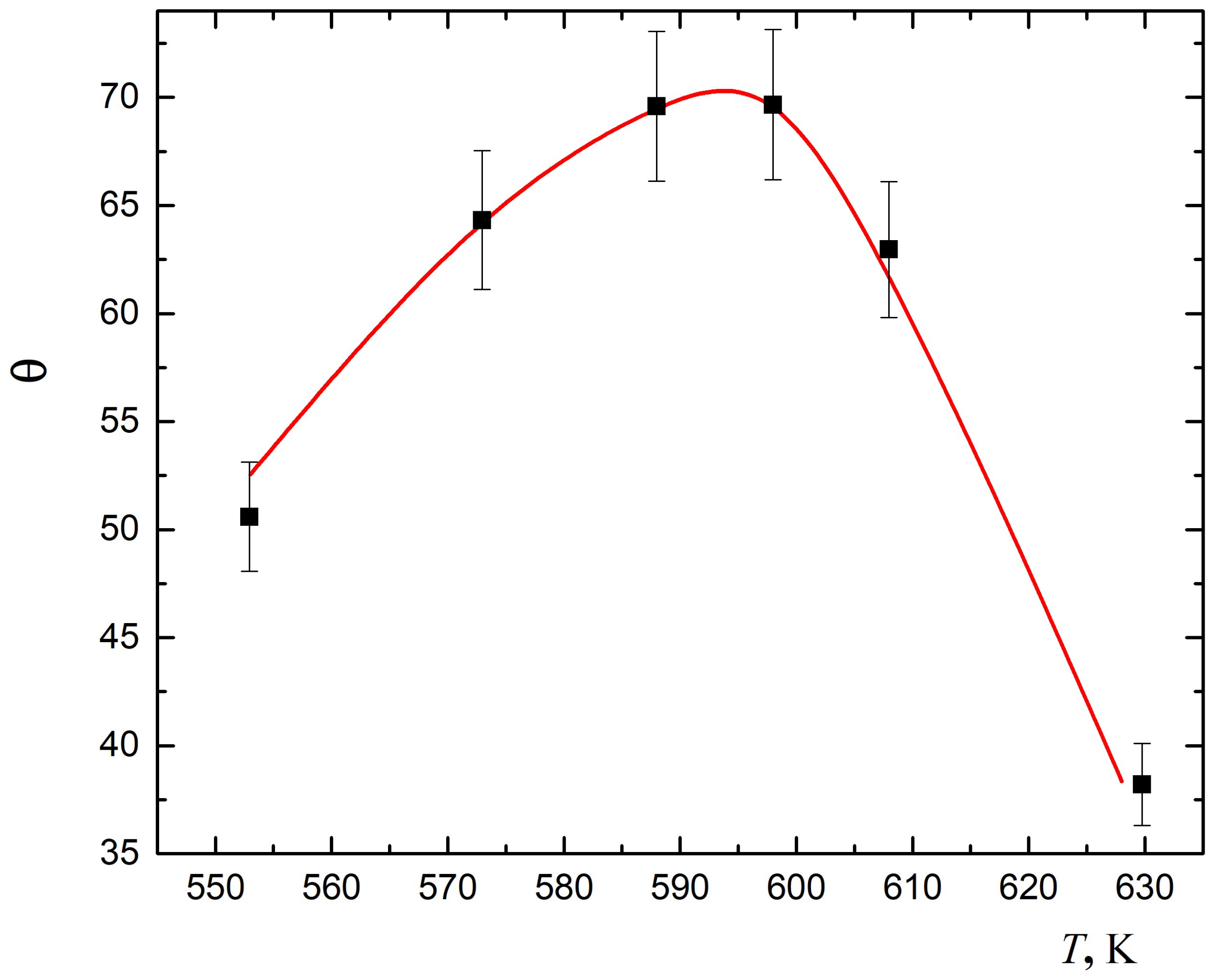
Figure 1 demonstrates good performance of the developed model for interpretation of experimental data on the dependence of the sensor effect (
) on temperature (
T). Details of the experiment are available in [
38]. The resistance of the film of
, laid over a dielectric substrate, was measured for the two cases: (i) in the stream of air, and (ii) in the stream of air with addition of
. The sensor effect is a ratio of these resistances. The measurements were conducted at various temperatures. The results were verified using five different samples of the film. The maximum error in resistance measurement was 2.5%.
Numerical experiments were conducted in order to achieve the best agreement with the experimental data. The values of the parameters delivering the best agreement are reported in
Table 4. These values have been partly extracted from existing publications, in particular, the measured values of the following: dielectric permittivity of nanoparticle material
, energy of donor level in the indium oxide
, density of donors
in the volume of a semiconductor nanoparticle, volume density of oxygen in the air
, frequency of stretching vibrations of atoms in adsorbed oxygen molecule
(of the order of
–
), and the energy required to tear off the molecule of oxygen from the surface of indium oxide
. Constants of the rate of the electron capture by the oxygen atom
and the reaction of hydrogen with adsorbed oxygen ions
were estimated directly from the experiments on kinetics of resistance variation upon the injection of hydrogen and oxygen. The rest of the parameter values were adopted based on the best agreement with the experimental data on the sensor effect to hydrogen.
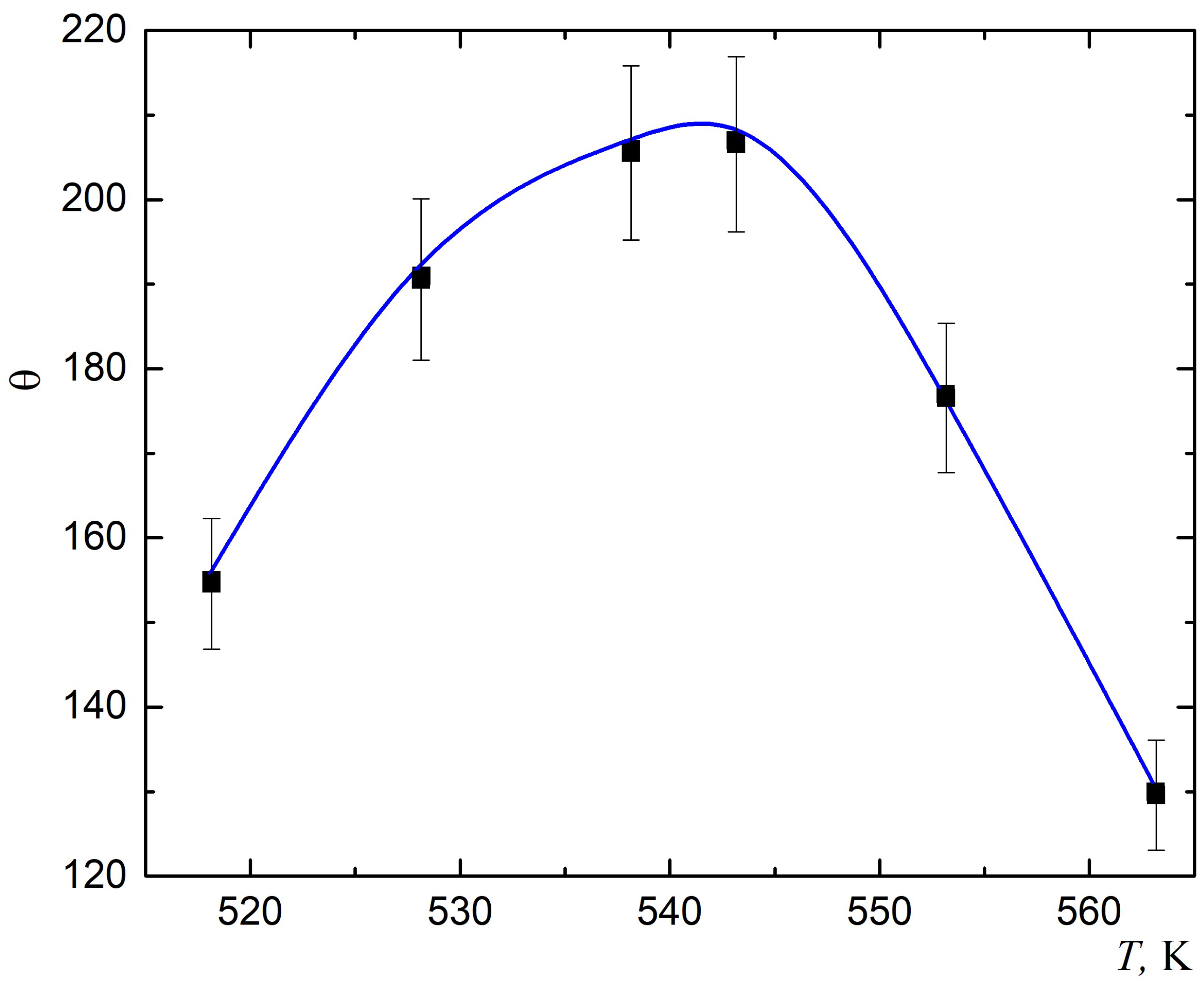
The developed technique for describing processes occurring in simple nanostructured materials also works in more complex cases. So, for illustration, in
Figure 2, the recently obtained results of comparing the theory with experimental data for the mixed system
-
[
39] is presented. The fitting procedure is slightly more complicated; along with processes (I)–(V), the chemical reactions on the surface of
nanoclusters and the transfer of reaction products to
nanoparticles should be taken into account. Accordingly, the system of kinetic equations will also change, but there are no fundamental innovations.


 ,
, 


