Article

Chaotic States of Transistor-Based Tuned-Collector Oscillator

Department of Radio Electronics, Faculty of Electrical Engineering and Communication, Brno University of Technology, Technicka 12, 616 00 Brno, Czech Republic
Mathematics 2023, 11(9), 2213; https://doi.org/10.3390/math11092213
Submission received: 16 April 2023 / Revised: 3 May 2023 / Accepted: 5 May 2023 / Published: 8 May 2023
(This article belongs to the Special Issue Mathematical Modeling and Simulation of Oscillatory Phenomena)

Abstract

:
This brief paper shows that robust chaotic behavior can be detected within a tuned-collector single-stage transistor-based oscillator. The content of this work also contributes to the problem of chaos localization in simplified mathematical model of standard analog building block. Searching for chaos is performed via numerical optimization routine applied onto the principal schematic of oscillator where generalized bipolar transistor is modelled as a two-port described by impedance as well as admittance matrix. In both cases, the presence of dense chaotic attractor is proved via calculation of the largest Lyapunov exponent, while its structural stability is validated by real measurement, i.e., visualization of captured oscilloscope screenshots.

1. Introduction

Chaos is a term that has many different interpretations based on the physical subject that generates it. If it relates to mathematical model expressed in the form of the ordinary differential equations, chaos can be understood as a long-term unpredictable evolution caused by the specific formation of vector field. The solution of chaotic system is very sensitive to small changes in initial conditions due to the exponential divergence of two neighboring state orbits. This feature of vector field is commonly denoted as stretching, while trajectory folding answers to intrinsic system nonlinearity and is responsible for strange attractor boundedness. The term strange attractor is also related to the subject of nonlinear dynamics, that is, we are speaking about the ω-limit set that comprises density and mixing.
Chaos belongs to a complex motion that can be revealed within very simple circuits, both autonomous and driven. To mention the famous example, isolated Chua’s oscillator contains only four linear passive components and one piecewise-linear [1] or cubic polynomial [2] active resistor. The same number of the passive elements and active two-port working in the trans-admittance mode with quadratic polynomial transfer function can lead to the steady state chaotic oscillations as well, as indicated in the paper [3]. These circuits belong to those that are deliberately constructed, with the knowledge of describing sets of ordinary differential equations as the robust chaos generators. However, chaos can be observed in the conventional non-chaotic building blocks dedicated for analogue signal processing. To find this kind of behavior, the initial step covers mathematical modeling of inspected dynamical system, considering an appropriately high level of abstraction. After that, elimination of nonessential parameters from the viewpoint of chaos evolution could be done. For example, fingerprints of deterministic chaos were reported in phase-locked loops [4], power converters [5], dc-dc converters [6], switching regulators [7], multi-state static memory cells [8], switched capacitor circuits [9], analog representation of simplified abandoned neuron [10], and many others.
This paper extends a list of typical sinusoidal oscillators forced into chaotic steady state, such as Colpitts [11], Hartley [12], or Wien bridge-based [13], Clapp [14], RC phase shift [15], by one additional case: single-stage tuned collector oscillator. Further text is organized as follows. The next section deals with numerical analysis of derived mathematical model which is, after removing parasitic properties of the generalized bipolar transistor, a third-order autonomous dynamical system in the dimensionless form. An active three-port, biased into hypothetical operating point, undergoes a multi-objective optimization routine. This results in a few sets of numerical values of internal parameters for which the oscillator becomes chaotic for all common perspectives: the positive largest Lyapunov exponent (LE), sensitivity to small changes of initial conditions, broad-band frequency spectrum, increased entropy of produced waveform, etc. Experimental construction and verification of flow-equivalent chaotic oscillator demonstrates, at least from the most interesting set of internal parameters, that chaos is neither a numerical artifact nor long transient behavior.

2. Mathematical Model of Single Transistor-Based Tuned-Collector Oscillator

The derivation process starts with a complete circuitry of this famous analog building block as depicted in Figure 1a. After removing parts dedicated to setup and stabilize bias point, we reached the most simplified structure in Figure 1b where only principal accumulation elements are presented. As a third step, assume the lossless transformer with voltage-current relations, namely
v C v X = L 1 d d t M d d t M d d t L 2 d d t · i 1 i 2 ,
where M is a mutual inductance of transformer and determines the coupling constant of transformer via formula k = M / L 1 · L 2 0 , 1 . Even though M is related to the physical construction of the feedback transformer, mutual inductance enters the optimization routine as a free parameter; how it works will be clarified later. Unfortunately, in practice, it is very difficult (almost impossible for hand-made realizations of transformers) to reach the exact value of M defined up to two decimal places.

2.1. Two-Port Model of Transistor Described by Impedance Parameters

If considered as two-port, a generalized bipolar transistor can be modelled by two-port impedance parameters, i.e., by following a pair of the algebraic equations
v b e = z 11 · i b + z 12 · i c , v c e = α · i b 3 + β · i b + z 22 · i c ,
where vbe and vce are base-emitter and collector-emitter voltages and ib and ic are the base and collector current, respectively. Forward trans-resistance is defined as a cubic polynomial function having odd symmetry z 21 i b = z 21 i b , without offset, and saturation shape is characterized by relation α < 0 , β > 0 . The circuit configuration depicted in Figure 1c) will be denoted as case Z, the state vector consists of circuit variables x = v C i 1 i 2 T , and can be described by the following system of first-order ordinary differential equations
d d t v C = 1 C · v C z 22 i 1 1 z 22 · α · i 2 3 + β · i 2 , d d t i 1 = 1 L 1 · v C + L 1 · M L 1 · L 2 M 2 · M L 1 + z 12 z 22 · v C z 11 · i 2 + z 12 z 22 · α · i 2 3 + β · i 2 , d d t i 2 = L 1 L 1 · L 2 M 2 · M L 1 + z 12 z 22 · v C z 11 · i 2 + z 12 z 22 · α · i 2 3 + β · i 2 ,
where M L 1 · L 2 is a mandatory condition. It should be noted that transformer’s full decoupling (value M = 0 H ) does not completely prevent the System (3) to behave chaotically since the accumulation elements are still coupled via forward and backward trans-impedance of the bipolar transistors. Regardless of the values of impedance parameters, state space origin is always the equilibrium point of this dynamical system. System (3) can possess two additional equilibrium points located symmetrically with respect to origin, namely in the following positions
z 0 = ± 1 a · z 12 · α · z 12 β · z 12 z 11 · z 22 , x 0 = L 1 z 12 α · z 0 3 + β · z 0 z 11 · z 22 · z 0 L 1 · z 12 + M · z 22 , y 0 = 1 z 22 x 0 + α · z 0 3 + β · z 0
The stability of fixed point located at the origin of the state space is determined by the eigenvalues, i.e., roots of characteristic polynomial
d e t λ · E J = λ 3 + 1 C · z 22 + L 1 z 22 · β · z 12 z 11 · z 22 M 2 L 1 · L 2 · λ 2 β · M + L 1 · z 11 + L 2 · z 22 + M · z 12 C · z 22 M 2 L 1 · L 2 · λ + β · z 12 z 11 · z 22 C · z 22 M 2 L 1 · L 2 = 0 ,
where E is unity matrix and J is Jacobi matrix. Since unstable equilibrium of any type is needed, polynomial (5) should be non-Hurwitz. Of course, in an optimization routine itself, numerical calculations are considered rather than symbolic calculations. For this dynamical system, the divergence of the vector field is also a watched function and can be established as
F = 1 C · z 22 + L 1 M 2 L 1 · L 2 z 11 z 12 z 22 · 3 · α · i 2 2 + β ,
i.e., calculated impedance parameters depend only on the state variable i2(t).

2.2. Two-Port Model of Transistor Described by Admittance Parameters

In this case, the global behavior of transistor is modelled by using admittance parameters calculated for the biasing point, that is, by two nonlinear equations
i b = y 11 · v b e + y 12 · v c e ,         i c = α · v b e 3 + β · v b e + y 22 · v c e .
Similarly, as it is for the previous case Z of the tuned-collector oscillator simplified schematic, the vector field is symmetrical with respect to origin and inequalities α < 0 , β > 0 applies. The circuit structure depicted in Figure 1d will be marked in further text as case Y, transistor part being dual to case Z dynamical system, state vector stands x = v C i 1 i 2 T , and can be described by the following system of ordinary differential equations
d d t v C = 1 C · y 22 · v C i 1 + α · y 12 · v C + i 2 y 11 3 + β · y 12 · v C + i 2 y 11 , d d t i 1 = L 1 · L 2 L 1 · L 2 M 2 · 1 L 1 M · y 12 L 1 · L 2 · y 11 · v C M y 11 · L 1 · L 2 · i 2 , d d t i 2 = L 1 · L 2 L 1 · L 2 M 2 · M L 1 · L 2 y 12 L 2 · y 11 · v C 1 L 2 · y 11 · i 2 .
This dynamical system always has equilibrium point located at the origin of the state space. It is also the only fixed point this system possesses. The stability of this fixed point and local geometry of neighborhood vector field is uniquely determined by eigenvalues, i.e., roots of characteristic polynomial
d e t λ · E J = λ 3 L 1 y 11 M 2 L 1 · L 2 + β · y 12 y 11 · y 22 C · y 11 · λ 2 β · M + L 2 · y 11 L 1 · y 22 + M · y 12 C · y 11 M 2 L 1 · L 2 · λ 1 C · y 11 M 2 L 1 · L 2 = 0 ,
During the search for chaos process, the numerical calculation of eigenvalues was preferred over the test if the polynomial (9) belonged to non-Hurwitz. At this point, continuation in symbolic calculations can be discontinued, as formulas for the eigenvalues are overly complicated long expressions. Note that attractors excited by fixed point at origin are sought after. Therefore, it is supposed that parameter values give rise to unstable equilibrium, having any type of local geometry and index of stability less than three. Speaking in terms of the optimization routine, the divergence of the vector field associated with this dynamical system also belongs to an important function. It can be calculated as
F = 1 C β · y 12 y 11 y 22 + 3 · α · y 12 i 2 + v C · y 12 2 y 11 3 + L 1 y 11 M 2 L 1 · L 2 ,
and generally depends on the state variables vC(t) and i2(t). However, for transistor without backward trans-conductance, function F is constant throughout state space and, as such, needs to be negative.

3. Searching for Chaos and Numerical Analysis

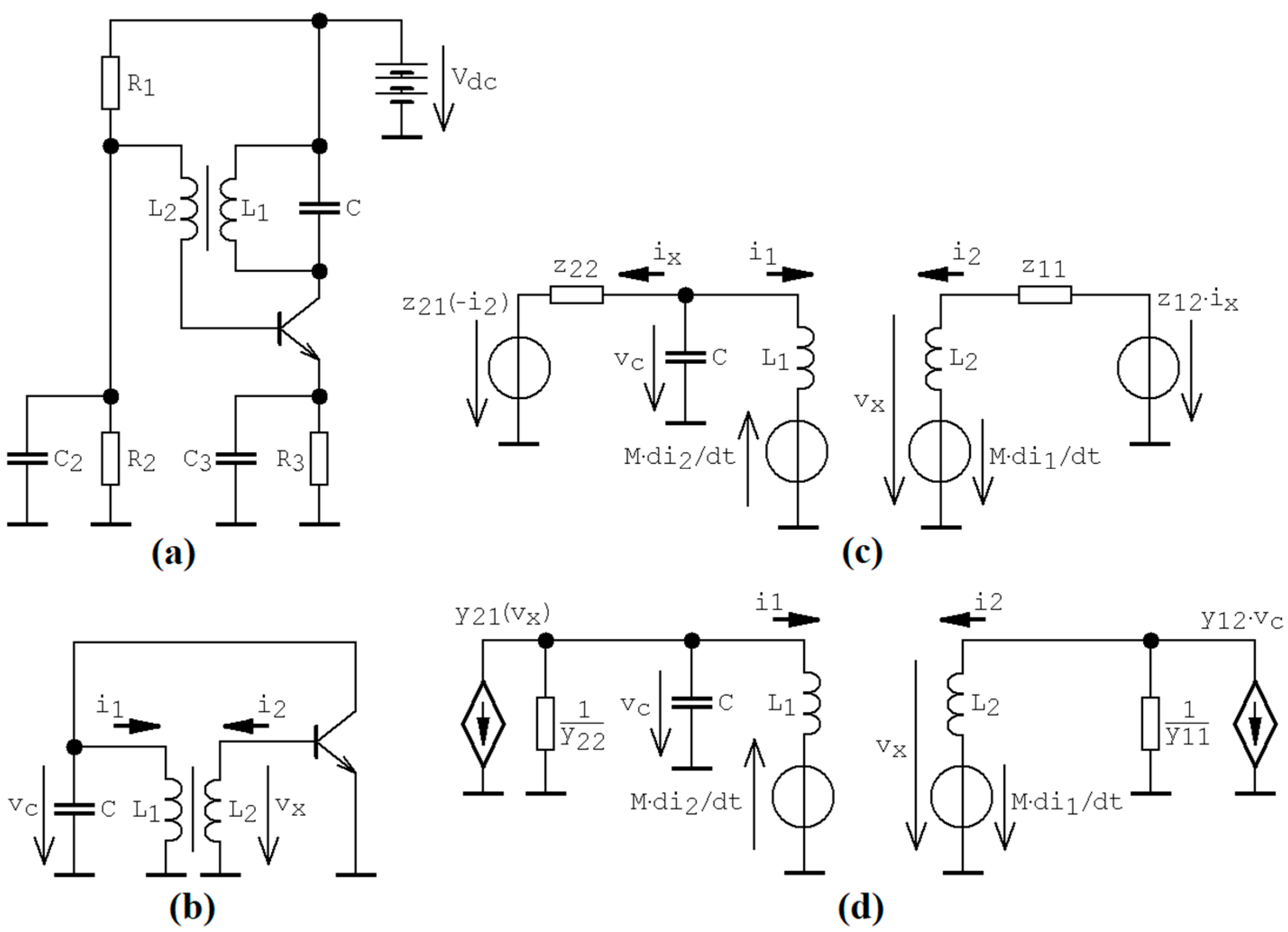
For further numerical analysis, the parameter constraints that reflect the conventional operational state of the sinusoidal oscillator should be considered. First of all, input and output impedance (case Z), as well as input and output admittance (case Y), will be positive numbers (zeroes are not excluded). Simultaneously, the backward trans-resistance (trans-conductance) should be as low as possible for case Z (case Y) dynamical system. Thanks to impedance and frequency rescaling, normalized values of all accumulation elements can be removed from the hyperspace of system parameters dedicated for optimization, i.e., we can keep them unified L 1 = L 2 = 1 H , C = 1 F . Additionally, it is quite complicated to realize the coupling coefficient k of a feedback transformer close to unity. Since k M , high values of the mutual inductance are penalized during optimization. Because of the nature of the search engine, where the initial conditions in each optimization step are chosen randomly in the vicinity of the state space, all strange attractors discovered and mentioned in this paper belong to the group of the self-excited attractors. Therefore, the existence of the so-called hidden attractors is not excluded.
As pointed out in papers [16,17,18,19,20], searching for the chaos process can be transformed into an optimization problem. In doing so, robust chaos was detected within the analyzed model of the tuned collector oscillator for the following mutual inductance and hypothetical bias point of the transistor modeled by impedance parameters
M = 0.75   H , z 11 = 0.33   Ω , z 12 = 0.3   Ω , z 22 = 1.45   Ω , α = 1   V 3 A 1 , β = 4.3   Ω .
For these values, the fixed point located at origin is a full repeller with a stability index of zero, characterized by the following eigenvalues λ 1,2 = 0.217 ± 2.851 j , λ 3 = 0.156 .
Within many runs of the search for chaos algorithm, another set of “chaotic system parameters” leading to geometrically different strange attractor was revealed, namely
M = 0.86   H , z 11 = 0.12   Ω , z 12 = 0.08   Ω , z 22 = 1.42   Ω , α = 1   V 3 A 1 , β = 4.1   Ω .
In this case, origin is a fixed point with stability index two, i.e., different local vector field geometry if compared to system with parameter set (8). Eigenvalues can be established as λ 1,2 = 0.154 ± 3.7251 j , λ 3 = 0.031 .
For transistor modeled using admittance parameters, the following group of the internal system parameters that leads to robust chaos was discovered
M = 0.49   H , y 11 = 3.3   S , y 12 = y 22 = 0   S , α = 10   A 3 V 1 , β = 15   S .
Note that, in this case, the transistor behaves close to an ideal current source without backward trans-conductance. This is an interesting situation since it is rather close to the conventional operation regime of sinusoidal oscillator. Sinusoidal oscillations with quite low harmonic distortion can be excited if forward transconductance of generalized transistor β < 10 S .
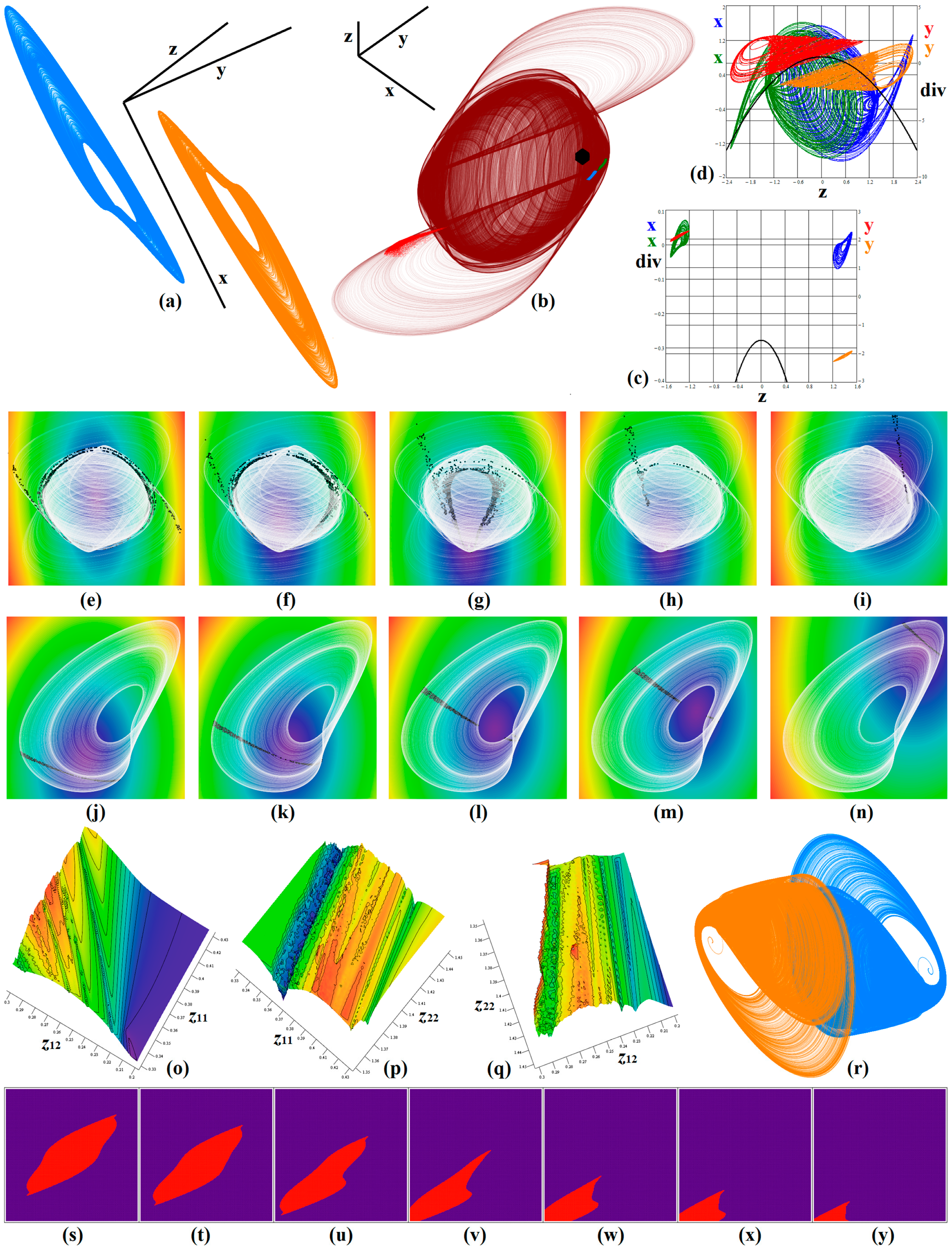
In the upcoming two figures, numerical integration results were obtained by using a fourth order Runge–Kutta method with final time 10,000 s and step size 10 ms. Note that step size is much smaller than the time constant of dynamical system expressed in terms of the eigenvalues [21]. Figure 2 brings selected results coming from the numerical analysis of case Z dynamical system. Namely, Figure 2a shows the typical shape of a strange attractor generated by parameter set (12) in full 3D perspective. The sets of initial conditions leading to proposed chaotic motions are x 0 = ± 0 2 1.5 T for orange and blue trajectory respectively. Figure 2b provides a typical strange attractor for parameter case (11). This plot also demonstrates the sensitive dependance of the solution to small perturbations of initial conditions. Small cubes with an edge of 0.01 (uniform distribution) containing 104 initial states were randomly generated (black dots). Following that, final states were stored after 2 s short-time evolution (blue dots), about 4 s average time evolution (green dots), and 10 s long-time evolution (red dots). Figure 2c,d show all plane projections of the typical strange attractor, together with a one-dimensional curve of divergence of the vector field as a function of state variable z(t). Figure 2d–m provide rainbow-scaled contour graphs of distribution of kinetic energy over the state space, calculated for time instance 100 ms and time step 1 ms. Cross-sections of generated attractors with individual horizontal planes of the state space were provided as well. Two-dimensional rainbow-scaled surface plots of the largest LE as function of bias point of the generalized transistor were provided via Figure 2n–p. There, strong chaos is marked by red color, weak chaos by yellow, a limit cycle using a green color, and the blue area corresponds to the trivial solution. Each high-resolution plot contains 101 × 101 = 10,201 points. Of course, only a very small fragment of hyperspace of the system parameters investigated by an optimization routine is visualized here. For a slightly increased normalized value of the input impedance, z11 = 0.33 Ω → 0.35 Ω of generalized transistor large attractor becomes separated into two funnel strange attractor, as illustrated in Figure 2q. Finally, Figure 2r,x provide basins of attraction for attractor generated by system (3) with parameter set (11). Each subplot represents horizontal planes where voltage across capacitor is constant, i1∈(–10, 10) A and i2∈(–10, 10) A. All initial states that eventually end up on the strange attractor are marked by red color, and the only other solution is unbounded (purple areas). Note that the basin for chaotic attractor fills an interestingly-shaped connected three-dimensional object in the state space.
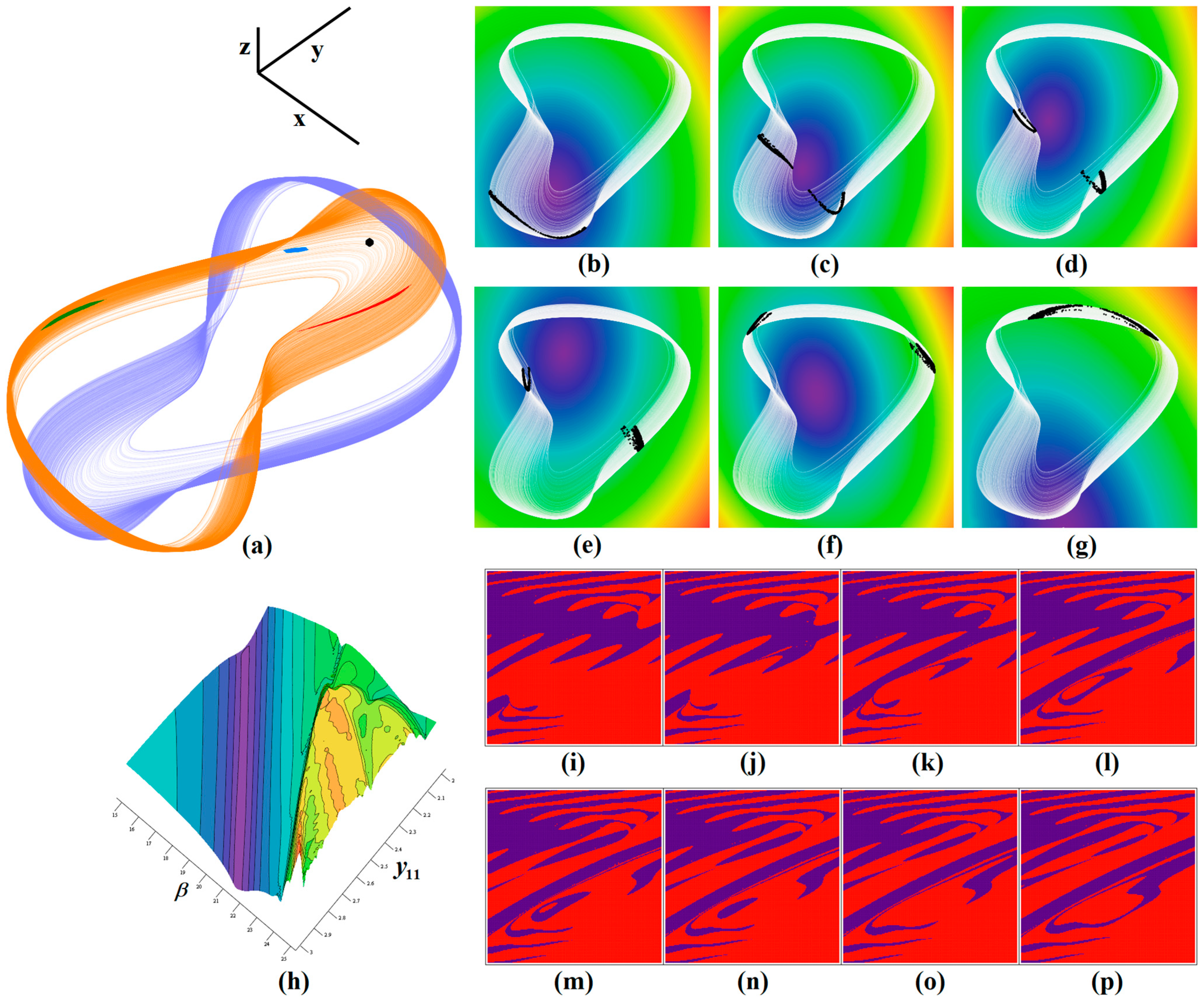
Figure 3 provides selected results coming from the numerical analysis of case Y dynamical system. The figure begins by showing two mirrored typical strange attractors obtained for initial conditions x 0 = 1.2 1 0 T for purple trajectory and x 0 = 1.2 1 0 T , leading to state attractor plotted using an orange color. This subplot also demonstrates the sensitivity of system solution to small differences in initial conditions. In the beginning, a group of 104 initial conditions with uniform distribution were placed about origin, forming a cube with an edge size of 0.01 (black points). After 2 s short-time evolution (blue dots), 4 s evolution (green dots), and 10 s long-time evolution (red dots), the final states were visualized. Figure 3b,g provide rainbow-scaled contour graphs showing distribution of kinetic energy over the state space, calculated for time instance 100 ms and time step 1 ms. Figure 3h shows the colored plot of the largest LE as a two-dimensional function of two system parameters. The area visualized here represents only a tiny fragment of hyperspace investigated by an optimization routine. Strong chaos is marked by a red color, weak chaos is marked by yellow, limit cycle uses a green color, and the blue area corresponds to the trivial solution. Each high-resolution plot contains 101 × 101 = 10,201 points.
Adopting “the most chaotic” numerical values revealed, the Kaplan–Yorke dimension of corresponding strange attractor approximately equals D K Y = 2.156 . The composition of plots in Figure 3i,p can be understood as slices of the state space, showing interesting geometric structure of basins of attraction that lead to the chaotic (red area) or unbounded (purple region) behavior. Each subplot represents horizontal planes where voltage across capacitor is constant, i1∈(–10, 10) A and i2∈(–10, 10) A. Note that only slices for positive values of voltage vC are provided. Because of vector field symmetry, the geometrical structure will be repeated for negative values.

4. Experimental Verification via Construction of Flow-Equivalent Oscillator

For research papers that present a new chaotic dynamical system, practical construction followed by experimental verification became the common standard long ago [22]. There are several reasons for this:
  • The trajectory that originates in numerical integration is subject to inevitable errors and represents only an approximation of real behavior, regardless of the method chosen.
  • A smooth integration process instead of problem discretization is performed using an electronic circuit.
  • With a suitable choice of time constant, we can easily decide if observed motion is a long transient or a robust, structurally stable solution.
  • Since individual bifurcation parameters can be associated with variable resistors, a smooth and wide change of its value can reveal dynamical phenomena unobserved during the numerical analysis, i.e., the behavior of chaotic circuit can be thoroughly studied without time-consuming re-simulations.
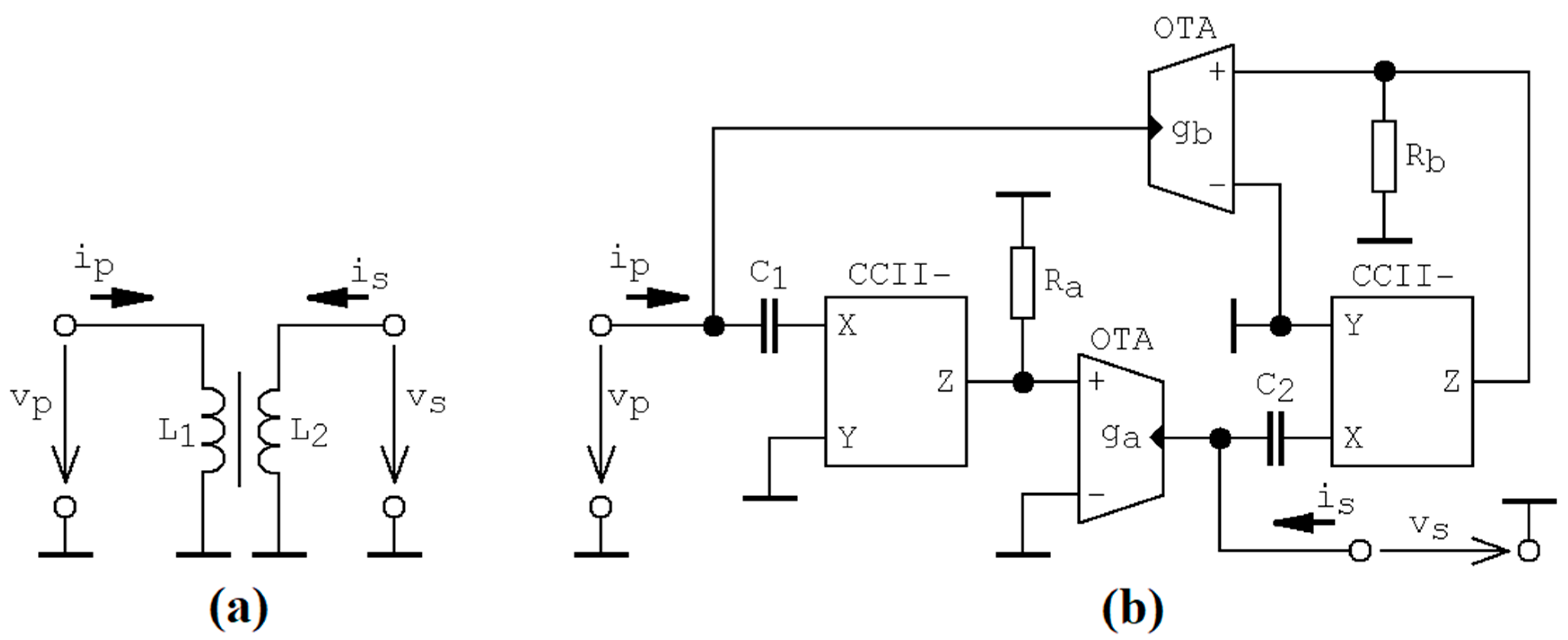
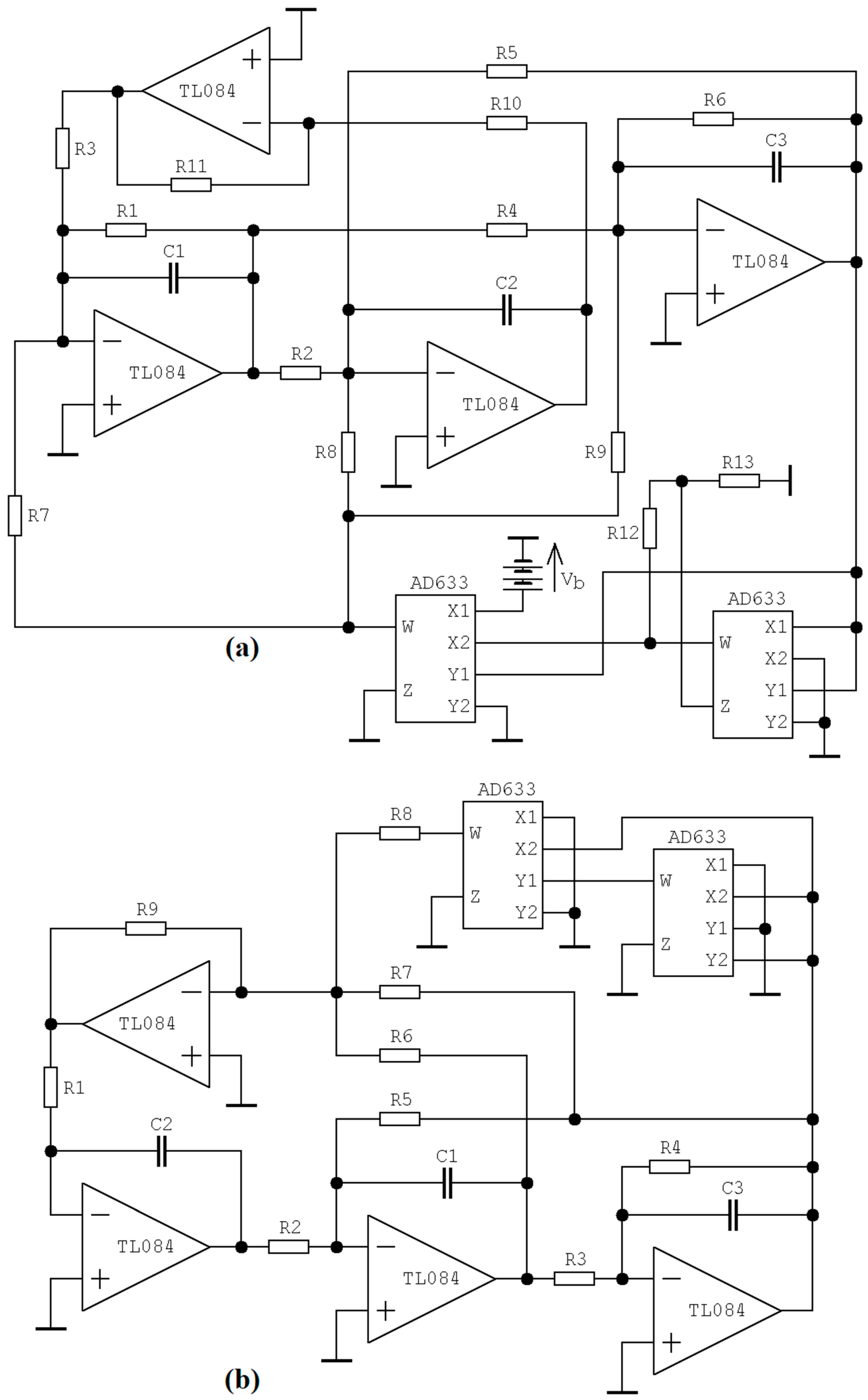
There are drawbacks that suggest that practical construction of transformer should be avoided: cumbersome realization of large values of self- and mutual inductances, hardly defined coupling coefficient, nonzero losses that can neither be precisely described nor included into the mathematical model. Assuming matrix Equation (1), the synthetic transformer suitable for our purposes can be designed, not directly, but considering ideal transformer´s dual circuit. Figure 4 shows two port circuit that behaves close to ideal transformer´s dual circuit. Moreover, the coupling coefficient is adjustable (or even electronically tunable using external DC voltage) via the main transfer constant of both operational trans-conductance amplifiers (OTA). Since admittance and impedance two-port models of transistor are dual by definition, synthetic transformer could be connected directly between the base and collector of modeled bipolar transistor. Accordingly, to a given schematic, this active device can be described by the following port equations
i p i s = d d t · C 1 d d t · C 2 · R b · g b · α 2 d d t · C 1 · R a · g a · α 1 d d t · C 2 · v p v s ,
where α1,2 are the current tracking errors of second-generation current conveyors (CCII–), ga and gb are trans-conductance of first and second OTA, respectively.
Although a synthetic ideal transformer with arbitrary mutual inductances can be designed as mentioned above, the necessity of four active devices appears to be an overly complicated circuit solution. For both Z and Y cases of analyzed dynamical system, a more promising way to model associated dynamics using lumped electronic circuits is the so-called analog computer concept [23,24]. This universal method is based on the complete knowledge of differential equations, i.e., including numerical values of the internal parameters. Only three basic building blocks are required for design: lossless inverting integrator, inverting summation amplifier and two-port with prescribed nonlinear transfer function: polynomial, piecewise-linear, or digitally synthesized [25]. For curious readers and design engineers, the latter publication source can be recommended; the cookbook is supported by complete documentation toward hybrid analog computer. Moreover, the time constant of the final circuit can be easily rescaled via simultaneous change of all capacitors.
A mathematical model (3) with numerical values (8) can be represented by a circuit provided in Figure 5a. The behavior of this oscillator is uniquely determined by the following set of ordinary differential equations
d d t v 1 = v 1 R 1 · C 1 + R 11 R 10 · R 3 · C 1 · v 2 K R 7 · C 1 · v 3 · V b K · v 3 2 , d d t v 2 = v 1 R 2 · C 2 v 3 R 5 · C 2 + K R 8 · C 2 · v 3 · V b K · v 3 2 , d d t v 3 = v 1 R 4 · C 3 v 3 R 6 · C 3 K R 9 · C 3 · v 3 · V b K · v 3 2 .
where K = 1/10 is internally trimmed transfer constant of the analog multiplier. State vector is composed by voltages measured at the outputs of inverting integrators. By comparing system (15) with model (3), together with parameters (11) and considering time constant τ = 100   μ s , we can establish numerical values of passive circuit components as
C 1 = C 2 = C 3 = 10   n F , R 1 = 14.3   k Ω , R 2 = 3.9   k Ω , R 3 = 10   k Ω , R 4 = 4.6   k Ω , R 5 = 18   k Ω , R 6 = 13.2   k Ω , R 7 = 143   Ω , R 8 = 278   Ω , R 9 = 208   Ω , R 10 = R 11 = 10   k Ω , R 12 = 1   k Ω , R 13 = 9   k Ω , V b = 430   m V .
Note that resistors R12 and R13 do not appear in differential equations since their purpose is compensation of transfer constant of first analog multiplier in cascade. When choosing time constant, the frequency limitations described in [26] associated with used active elements need to be considered.
Similarly, case Y dynamical system can be modeled by electronic network given in Figure 5b, and the corresponding system of ordinary differential equations is
d d t v 1 = v 2 R 1 · C 1 v 3 R 2 · C 1 + K 2 R 9 · C 1 · v 3 3 ,         d d t v 2 = R 5 R 6 · C 2 · v 1 R 3 + v 2 R 2 + v 3 R 4 ,         d d t v 3 = v 1 R 7 · C 3 v 3 R 8 · C 3
Numerical values of circuit elements can be calculated using direct comparison between system (17), with its mathematical model (8) having parameters (13) and considering the time scale τ = 100   μ s as follows
C 1 = C 2 = C 3 = 10   n F , R 1 = R 2 = 1   k Ω , R 3 = 15.5   k Ω , R 4 = 25   k Ω , R 5 = 2.2   k Ω , R 6 = 7.6   k Ω , R 7 = 51   k Ω , R 8 = 360   Ω , R 9 = 10   k Ω .
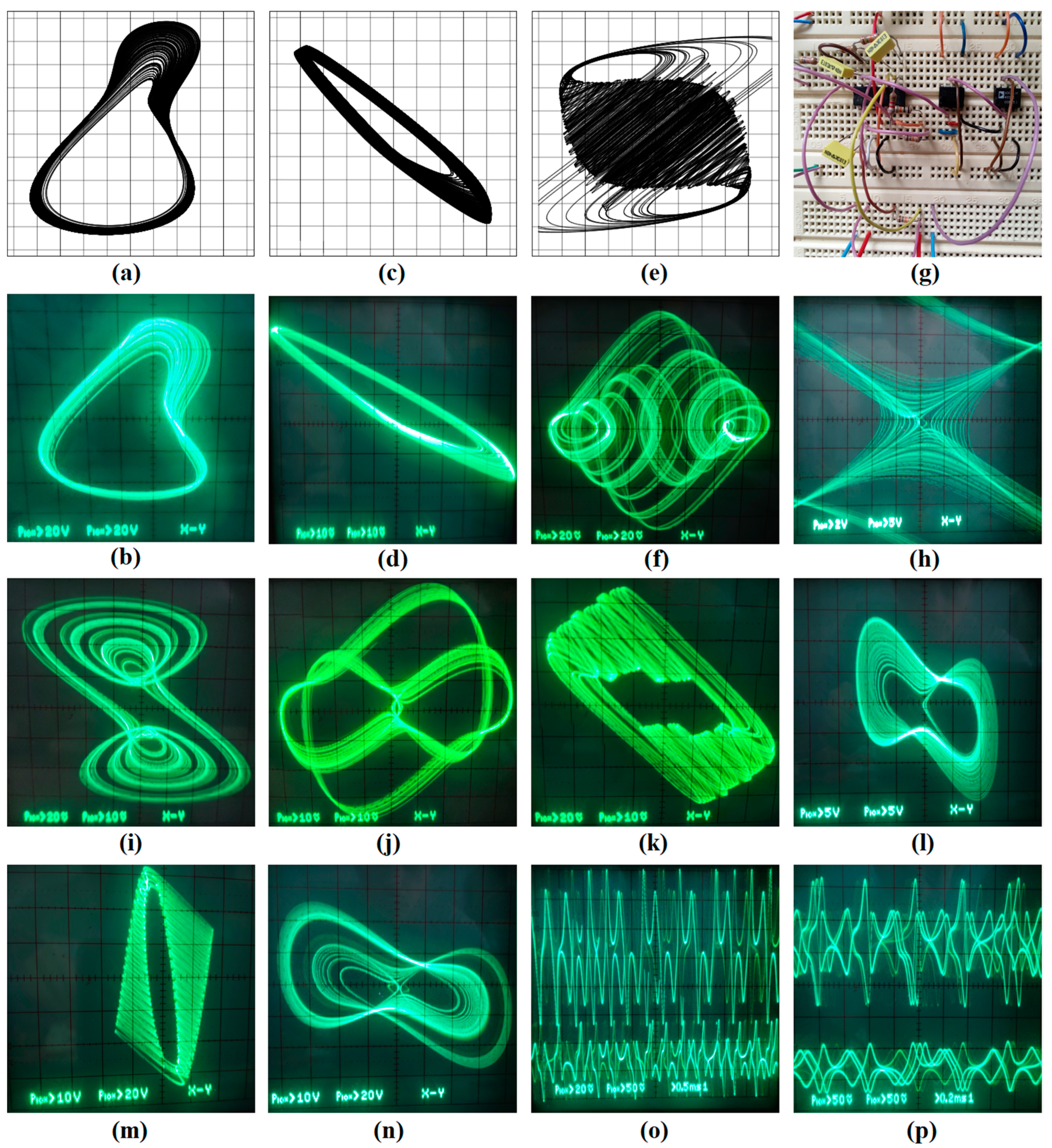
Note that both oscillators are quite simple, with only three integrated circuits fed by the symmetrical ±15 V supply voltage. A few examples coming from laboratory experiments can be found in Figure 6, including breadboard photo (Figure 6g) and waveforms captured in time domain (Figure 6o,p). Designed chaotic oscillators proves useful for finding strange attractors that were unnoticed during numerical analysis (Figure 6i–n).

5. Discussion

The importance of this paper is to show that the circuitry realization of tuned collector sinusoidal oscillator could be the subject of robust chaotic dynamics. Chaos can be observed both numerically and experimentally for an oscillator that has transistor modeled by impedance or admittance two-port parameters. For chaotic regimes, system parameters have physically reasonable numerical values that are not far away from some application-specific operational states. However, specific biasing of bipolar transistor (and utilization of transistor itself) is avoided by the circuit synthesis method based on an integrator block schematic associated with the mathematical model. Several interestingly-shaped strange attractors were discovered and captured using an oscilloscope.

6. Conclusions

Modern personal computers provide high computational power allow chaos (and hyperchaos) localization within the lower-dimensional dynamical system. However, when investigating real signal processing functional blocks, the number of “unknown parameters” needs to be reduced to maintain solvability of this problem. Search routine optimization with respect to parallel processing is a good idea when working toward significant reduction of time demands. When “chaotic parameters” are found, detailed numerical analysis is still needed to confirm robust chaos and recognize its properties.
This paper contributes to this issue with another successive chaos localization—inside tuned collector transistor-based oscillator. The list of chaotic oscillators that originate in the mathematical model of simplified electronic systems will undoubtedly grow in the near future. Considering the fractional-order nature of some accumulation elements (with transformer being a nice challenge) represents an area for further research.

Funding

This research was funded by Brno University of Technology, specific research grant number FEKT-S-23-8191.

Data Availability Statement

No data were created in the frame of this paper.

Acknowledgments

I would like to thank my student, Miroslav Rujzl, for his assistance during experimental verification of chaotic oscillators designed as analog computers.

Conflicts of Interest

The author declares no conflict of interest.

References

  1. Matsumoto, T. A chaotic attractor from Chua’s circuit. IEEE Trans. Circuits Syst. 1984, 31, 1055–1058. [Google Scholar] [CrossRef]
  2. Zhong, G.Q. Implementation of Chua’s circuit with a cubic nonlinearity. IEEE Trans. Circuits Syst. I Fundam. Theory Appl. 1994, 41, 934–941. [Google Scholar] [CrossRef]
  3. Petrzela, J.; Polak, L. Minimal realizations of autonomous chaotic oscillators based on trans-immittance filters. IEEE Access 2019, 7, 17561–17577. [Google Scholar] [CrossRef]
  4. Endo, T.; Chua, L.O. Chaos from phase-locked loops. IEEE Trans. Circuits Syst. 1988, 35, 987–1003. [Google Scholar] [CrossRef]
  5. Hamill, D.C.; Jeffries, D.J. Subharmonics and chaos in a controlled switched-mode power converter. IEEE Trans. Circuits Syst. 1988, 35, 1059–1061. [Google Scholar] [CrossRef]
  6. Deane, J. Chaos in a current-mode controlled boost DC-DC converter. IEEE Trans. Circuits Syst. I Fundam. Theory Appl. 1992, 39, 680–683. [Google Scholar] [CrossRef]
  7. Tse, C.K. Flip bifurcation and chaos in three-state boost switching regulators. IEEE Trans. Circuits Syst. I Fundam. Theory Appl. 1994, 41, 16–23. [Google Scholar] [CrossRef]
  8. Petrzela, J. Multi-valued static memory with resonant tunneling diodes as natural source of chaos. Nonlinear Dyn. 2018, 94, 1867–1887. [Google Scholar] [CrossRef]
  9. Rodriguez-Vazquez, A.; Huertas, J.; Chua, L.O. Chaos in switched-capacitor circuit. IEEE Trans. Circuits Syst. 1985, 32, 1083–1085. [Google Scholar] [CrossRef]
  10. Petrzela, J.; Hrubos, Z.; Gotthans, T. Modeling deterministic chaos using electronic circuits. Radioengineering 2011, 20, 438–444. [Google Scholar]
  11. Kennedy, M.P. Chaos in the Colpitts oscillator. IEEE Trans. Circuits Syst. I Fundam. Theory Appl. 1994, 41, 771–774. [Google Scholar] [CrossRef]
  12. Kvarda, P. Chaos in Hartley’s oscillator. Int. J. Bifurc. Chaos 2011, 12, 2229–2232. [Google Scholar]
  13. Elwakil, A.S.; Kennedy, M.P. A family of Wien-type oscillators modified for chaos. Int. J. Circuit Theory Appl. 1997, 25, 561–579. [Google Scholar] [CrossRef]
  14. Petrzela, J. Chaotic and hyperchaotic dynamics of a Clapp oscillator. Mathematics 2022, 10, 1868. [Google Scholar] [CrossRef]
  15. Hosokawa, Y.; Nishio, Y.; Ushida, A. Analysis of chaotic phenomena in two RC phase shift oscillators coupled by a diode. IEICE Trans. Fundam. 2001, E84-A, 2288–2295. [Google Scholar]
  16. Jafari, S.; Sprott, J.C.; Pham, V.-T.; Golpayegani, S.M.R.H. A new cost function for parameter estimation of chaotic systems using return maps as fingerprints. Int. J. Bifurc. Chaos 2014, 24, 1567–1580. [Google Scholar] [CrossRef]
  17. Nuñez-Perez, J.-C.; Adeyemi, V.-A.; Sandoval-Ibarra, Y.; Perez-Pinal, F.-J.; Tlelo-Cuautle, E. Maximizing the chaotic behavior of fractional order Chen system by evolutionary algorithms. Mathematics 2021, 9, 1194. [Google Scholar] [CrossRef]
  18. Adeyemi, V.-A.; Tlelo-Cuautle, E.; Perez-Pinal, F.-J.; Nuñez-Perez, J.-C. Optimizing the maximum Lyapunov exponent of fractional order chaotic spherical system by evolutionary algorithms. Fractal Fract. 2022, 6, 448. [Google Scholar] [CrossRef]
  19. Petrzela, J. Optimal piecewise-linear approximation of the quadratic chaotic dynamics. Radioengineering 2012, 21, 20–28. [Google Scholar]
  20. Silva-Juarez, A.; Tlelo-Cuautle, E.; Gerardo de la Fraga, L.; Li, R. Optimization of the Kaplan-Yorke dimension in fractional-order chaotic oscillators by metaheuristics. Appl. Math. Comput. 2021, 394, 125831. [Google Scholar] [CrossRef]
  21. Valencia-Ponce, M.A.; Tlelo-Cuautle, E.; Gerardo de la Fraga, L. Estimating the highest time-step in numerical methods to enhance the optimization of chaotic oscillators. Mathematics 2021, 9, 1938. [Google Scholar] [CrossRef]
  22. Sprott, J.C. A proposed standard for the publication of new chaotic systems. Int. J. Bifurc. Chaos 2011, 21, 2391–2394. [Google Scholar] [CrossRef]
  23. Itoh, M. Synthesis of electronic circuits for simulating nonlinear dynamics. Int. J. Bifurc. Chaos 2001, 11, 605–653. [Google Scholar] [CrossRef]
  24. Petrzela, J.; Gotthans, T.; Guzan, M. Current-mode network structures dedicated for simulation of dynamical systems with plane continuum of equilibrium. J. Circuits Syst. Comput. 2018, 27, 1830004. [Google Scholar] [CrossRef]
  25. Rujzl, M.; Polak, L.; Petrzela, J. Hybrid analog computer for modeling nonlinear dynamical systems: The complete cookbook. Sensors 2023, 23, 3539. [Google Scholar] [CrossRef]
  26. Munoz-Pacheco, J.M.; Tlelo-Cuautle, E.; Toxqui-Toxqui, I.; Sanchez-Lopez, C.; Trejo-Guerra, R. Frequency limitations in generating multi-scroll chaotic attractors using CFOAs. Int. J. Electron. 2014, 101, 1559–1569. [Google Scholar] [CrossRef]
Figure 1. Single transistor-based tuned-collector oscillator: (a) network ready for practical application, (b) simplified calculation schematic, (c) calculation model with transistor modeled by impedance parameters, (d) calculation schematic considering two-port admittance parameters. Open arrow marks orientation of voltage, short thick arrow represents orientation of current.
Mathematics 11 02213 g001
Figure 2. Numerical integration process using: (a) parameters (12), (b) parameters (11), and showing sensitive dependance on the initial conditions. Plane projections of generated strange attractor and divergence of vector field (black curve) plotted for: (c) parameters (12), (d) parameters (11). Distribution of kinetic energy over state space and Poincaré return maps for parameter set (11) and planes: (e) i2 = 0 A, (f) i2 = 500 mA, (g) i2 = 1 A, (h) i2 = 1.5 A, (i) i2 = 2.3 A. Poincaré sections for parameter set (12) and planes: (j) i2 = 1.25 A, (k) i2 = 1.3 A, (l) i2 = 1.36 A, (m) i2 = 1.45 A, (n) i2 = 1.5 A. Surface plots of the largest LE as function of bias point: (o) z11 vs. z12, (p) z11 vs. z22, (q) z12 vs. z22. Plot (r) shows structure of two unmerged strange attractors for slightly increased input impedance z11 = 0.35 Ω excited by external fixed points. Basin of attraction for: (s) vC = 0 V, (t) vC = 2 V, (u) vC = 4 V, (v) vC = 6 V, (w) vC = 8 V, (x) vC = 10 V, (y) vC = 12 V.
Mathematics 11 02213 g002
Figure 3. Numerical integration procedure: (a) evolution of two chaotic attractors symmetrical with respect to origin. Distribution of kinetic energy over the state space and Poicaré sections for planes: (b) i2 = –3 A, (c) i2 = –1 A, (d) i2 = 0 A, (e) i2 = 1 A, (f) i2 = 4 A, (g) i2 = 5 A. Subplot (h) shows rainbow-scaled surface plot of the largest LE as function of transistor´s bias point plotted with respect to y11 vs β. Basins of attraction calculated for planes: (i) vC = 0 V, (j) vC = 2 V, (k) vC = 4 V, (l) vC = 6 V, (m) vC = 7 V, (n) vC = 8 V, (o) vC = 9 V, (p) vC = 10 V.
Mathematics 11 02213 g003
Figure 4. Feedback transformer: (a) original conventional realization, (b) dynamically equivalent dual two-port network with electronically reconfigurable parameters of admittance matrix.
Mathematics 11 02213 g004
Figure 5. Analog computer-based lumped circuitry realizations of discovered chaotic dynamical systems: (a) case Z, (b) case Y.
Mathematics 11 02213 g005
Figure 6. Selected results coming from detailed experimental verification through measurement. Dynamical system case Y: (a) numerical integration of the typical strange attractor, (b) corresponding measurement in the same plane projection. Dynamical system case Z: (c,d) numerical integration of typical chaotic attractor visualized using different plane projections, (e,f) corresponding captured oscilloscope screenshots using the same state space planes, (g) breadboard realization showing great simplicity of final chaotic oscillator, (h) state trajectories zoomed near the unstable fixed point located at origin, (in) observed robust chaotic attractors that were unnoticed during numerical analysis, (o,p) chaotic waveform in time domain captured in different time intervals.
Mathematics 11 02213 g006
Disclaimer/Publisher’s Note: The statements, opinions and data contained in all publications are solely those of the individual author(s) and contributor(s) and not of MDPI and/or the editor(s). MDPI and/or the editor(s) disclaim responsibility for any injury to people or property resulting from any ideas, methods, instructions or products referred to in the content.

