Article

Adaptive Controller for Bus Voltage Regulation on a DC Microgrid Using a Sepic/Zeta Battery Charger/Discharger

by
Jhoan Alejandro Montenegro-Oviedo
1,
Carlos Andres Ramos-Paja
2,
Martha Lucia Orozco-Gutierrez
1,*,
Edinson Franco-Mejía
1 and
Sergio Ignacio Serna-Garcés
3
1
Escuela de Ingeniería Eléctrica y Electrónica, Universidad del Valle de Colombia, Cali 760042, Colombia
2
Facultad de Minas, Universidad Nacional de Colombia, Medellin 050041, Colombia
3
Departamento de Electrónica y Telecomunicaciones, Instituto Tecnológico Metropolitano, Medellin 050013, Colombia
*
Author to whom correspondence should be addressed.
Mathematics 2023, 11(4), 793; https://doi.org/10.3390/math11040793
Submission received: 27 December 2022 / Revised: 27 January 2023 / Accepted: 3 February 2023 / Published: 4 February 2023
(This article belongs to the Special Issue Analysis and Control of Dynamical Systems)

Abstract

:
In a DC microgrid that involves a battery storage system, the primary energy management is performed by a battery charger/discharger based on a dc/dc power converter. Moreover, the battery charger/discharger is also used to regulate the voltage of the dc bus. One of the challenges at the control level is to regulate the DC bus voltage under battery charge and discharge conditions but also under different relations between the battery and bus voltages. For this reason, this paper proposes a battery charger/discharger based on the Sepic/Zeta converter and an adaptive controller, which provides bidirectional current flow, stable bus voltage, and satisfactory electrical characteristics. The main advantage of the proposed control system is the capability to adapt the controller parameters to any operation condition, which provides a general solution to interface any battery to any bus voltage. This study is focused on the design procedure of both the power converter and the controller, where a detailed mathematical analysis is performed to ensure the system performance and stability. Finally, the proposed solution is validated using an experimental prototype and a practical application case.

1. Introduction

There is a fast growth of renewable energy installations due to increased energy demand and the need to reduce the use of fossil fuels [1]. However, the intermittent nature of renewable energy, for instance, solar and wind power, does not allow these installations to provide energy continuously for 24 h a day and it is necessary to store it for later use. Therefore, an energy storage system (ESS) widely used is the battery (BESS) [2,3,4], which, due to its high energy density, can store the energy of the distributed energy sources (DES) and deliver it to the loads, thus forming a microgrid (MG) [5]. These microgrids increase the reliability and controllability of the electrical system [6].
The fluctuations of the MGs due to the generation and the demand should be compensated, and it is here where the BESS plays an important role. The interface between the BESS and the system bus is a power converter, which manages the missing energy or surplus of sources concerning demand [7]. If the bus is a DC bus, then a DC/DC power converter with bidirectional power flow that can guarantee the polarity of both battery and DC bus and that offers conversion rates that allow a step-down and step-up of the voltage will be used. Different power converter topologies, such as buck/boost, Sepic, flyback, and Zeta, have been used to connect BESSs to DC buses. These power converters aim to charge and discharge the BESS and control characteristics such as voltage, current ripple, current increase rate, and more. For example, a regulated DC bus voltage facilitates the source’s power extraction and guarantees a high-quality power to the loads along with the low current ripple. Likewise, low current ripple and low current increase rates augment the battery lifetime.
Many works about bidirectional converters have been found during a state-of-the-art review. For example, ref. [8] provided a survey from the point of view of the topology and control scheme. This work divided the converters into nonisolated and isolated bidirectional converters, but the analyses did not show their use as an interface between BESS and DC buses.
The most common bidirectional converter is the buck/boost type. It is used for MPPTs (maximum power point trackers) in solar systems [9] and DC bus regulation in MGs with a sliding-mode controller (SMC) [10,11], with a PI classical controller [12], or with a model predictive control (MPC) using a dynamic reference [13]. Similarly, such a solution was also implemented with a hybrid energy storage system using a sliding-mode current controller on a fifth-order averaged model as reported in [14]. Moreover, the work reported in [15] developed a high-gain sliding controller acting on a supercapacitor, and in [16], a sliding-mode controller of the electromechanical actuator’s (EMA) current of an aircraft powered by a supercapacitor was discussed. Other works have been based on sliding-mode current controllers operating with supervisory strategies to act on the state-of-charge (SOC) of the battery, its charge/discharge current, the regulation of the high-voltage side, or to maximize the generator current [17,18,19,20,21,22]. Moreover, some variants exist. First, ref. [23] introduced a bidirectional converter with a coupled inductor used to charge/discharge an EV (electrical vehicle) battery and regulate the DC bus voltage together with fuzzy control. The second was a variant integrated by two buck/boost converters in cascade and an auxiliary capacitor that reduced the output current ripple and increased the efficiency, which used a PI controller to regulate the output voltage in a photovoltaic and energy storage system [24]. The third was a bidirectional converter for the DC bus and battery bank interface in a UPS (uninterruptible power supply) with an auxiliary commutation circuit [25,26]. The control system was composed of four independent controllers (classical P, PI, and average current), which had to control the charge of the battery bank, regulate the output voltage, and ensure the unitary input power factor.
On the other hand, Cuk bidirectional converters have been used to charge/discharge batteries with a PI controller for an average inductor current in [27] and DC bus voltage regulation with limiters of current and voltage in [28].
Moreover, the bidirectional flyback dc–dc converter is frequently used to interface BESSs and DC links. Ref. [29] presented a multiport flyback with a simple hysteresis voltage control to regulate the DC link voltage of an EV, and ref. [30] showed a flyback converter for use as a mobile phone charger with current and voltage regulation using a classical PI controller. Moreover, refs. [31,32] used the bidirectional flyback converter as a Li-ion battery cell current equalizer.
This manuscript deals with the Sepic/Zeta bidirectional converter and its use as a power manager between a BESS and the DC bus of an MG. This converter is used in different applications, for example, to interface PEVs (plug-in electric vehicles) to a charger station and to charge/discharge an ESD (energy storage device) in an MG. Nevertheless, there are few works on the Sepic/Zeta bidirectional converter as charger/discharger of BESSs.
Ref. [33] proposed an ESDs charging/discharging system designed to regulate the voltage of a DC bus using an SMC controller on a switched model of a Sepic/Zeta bidirectional converter. The DC bus voltage error and the currents of both converter inductors formed the switching function, guaranteeing a state–stable voltage error of zero and the global stability of the system. One of the three switching function parameters was calculated online for stability proposes. The other two were calculated offline according to closed-loop dynamics to provide a null voltage overshoot and a fast bus voltage restoration after transients.
Ref. [34] presented a DC–DC bidirectional Sepic/Zeta converter with a model of the averaged state space. The converter managed the power interchange between a BESS and a DC bus, and it was controlled by an adaptive SMC to improve the transient and steady-state behavior. The DC bus voltage error and the currents of both the battery side capacitor and the DC bus side capacitor formed the switching function. The results were compared against a PID classical controller, and the overall dynamic performance was significantly improved, guaranteeing the system’s global stability.
Ref. [35] presented a bidirectional converter in a PEV working in three modes: plug-in charging, propulsion, and regenerative. The control system consisted of three classical PI controllers: two to regulate the input and battery currents and one to regulate the motor voltage.
Ref. [36] showed a charging/discharging system for a BESS using a bidirectional DC–DC Sepic/Zeta converter with a PID (proportional–integral–derivative) controller for the voltage management of a DC bus. The converter’s state-space circuit-averaged-modeling-based transfer function approach was presented to control the switching pulses in both Sepic and Zeta modes. The classical Ziegler–Nichols method was used to design the controller, and a PSO (particle swarm optimization) tool was used to tune it. However, this work did not use robust adaptative control or perform any experimental validation.
Some works showed a variant of the Sepic/Zeta bidirectional converter with advantages such as low switching and conduction losses [37,38] and low-ripple currents [39]. However, they did not provide any evidence of their application as the interface between a BESS and DC bus with an adaptive control scheme.
This article proposes a state feedback linear quadratic Gaussian (LQG) adaptative strategy, which aims to regulate the MG’s DC bus voltage in any system operating conditions. For example, the battery can be in charge, discharge, or standby mode (when there is no interchange energy between the battery and the DC bus), and the Sepic/Zeta bidirectional converter can be a step-down (buck mode), a step-up (boost mode), or with a unitary conversion relation (unitary gain mode). The strategy above is applied to the charger/discharger Sepic/Zeta bidirectional converter, which is modeled with an averaged state-space small-signal model. This model is necessary since the LQG controller requires a linearized model. For this, three control blocks are used: a linear quadratic integral (LQI) controller to regulate the DC bus voltage, an optimal observer to estimate the system states, and an adaptive law to adjust the LQI parameters. Experimental validation only requires the measurement of two voltages: the DC bus and battery voltages.
The works in [33,34] are similar to the one presented here; however, ref. [33] introduced a system with a switched model and a sliding-mode controller, and its implementation required the measurement of two voltages, the DC bus and battery voltages, and the currents of both inductors. While the authors in [34] proposed a system with a state-space averaged modeling and an adaptive SMC. Their implementation required the measurement of two voltages, the DC bus and battery voltages, and four currents, the DC bus current, battery current, and capacitors current of both sides of the DC bus and the battery.
This work is split into six sections: the control-oriented modeling and design of the Sepic/Zeta converter, the design of the state-observer and the adaptive LQI controller, a test case with simulation results that include all operating modes of the battery and Sepic/Zeta converter, an experimental validation with all simulated cases, and finally the conclusions.

2. Modeling and Design of the Power Stage

This section describes the power stage circuit, the mathematical model and the design procedure of the electrical elements.

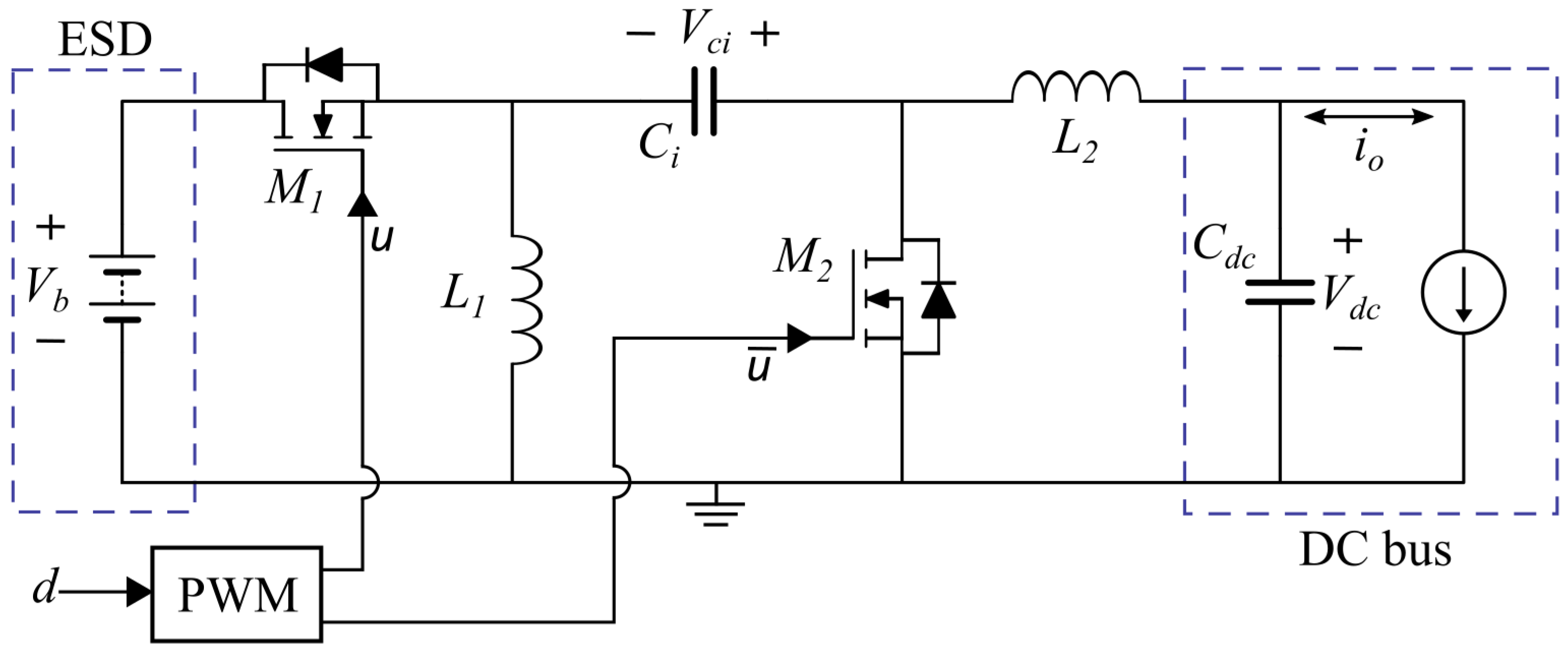
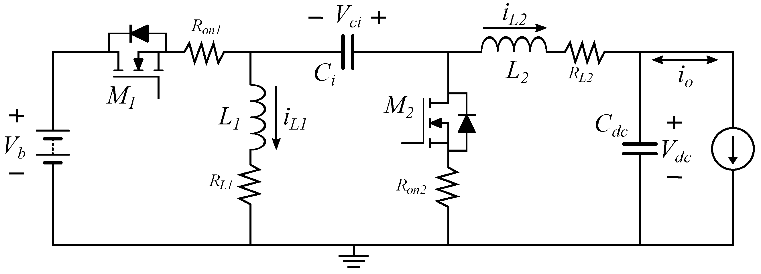
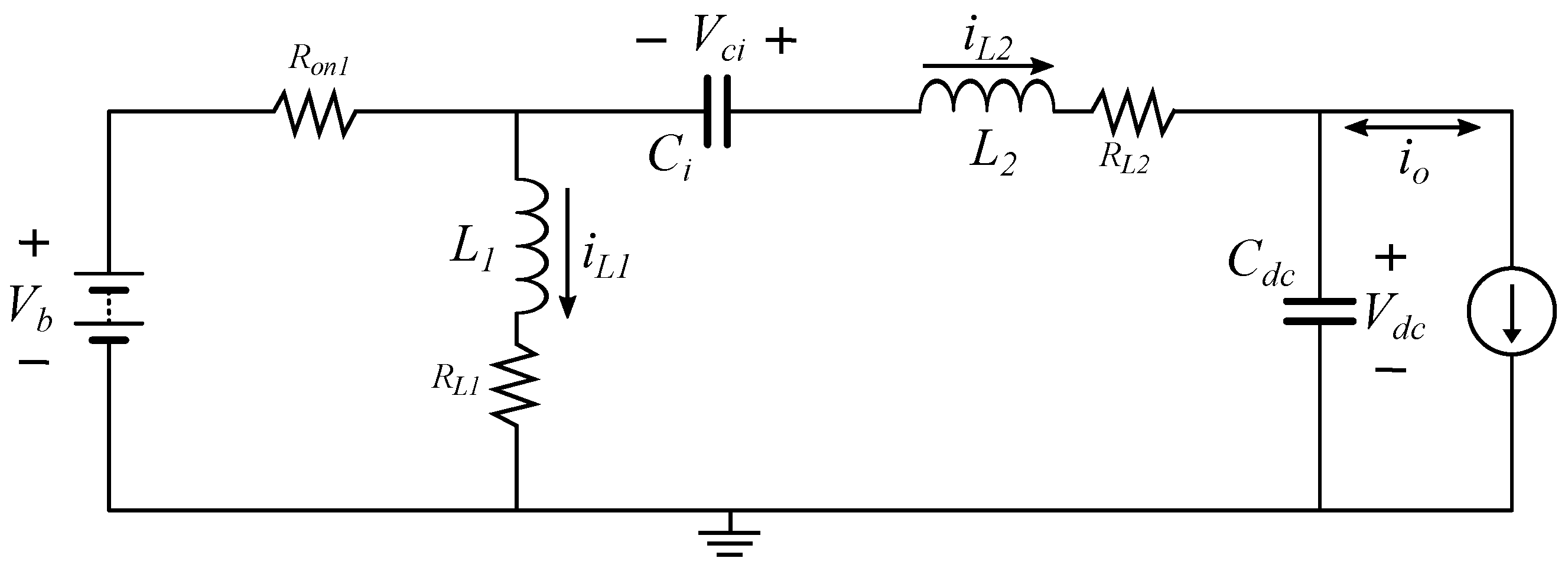
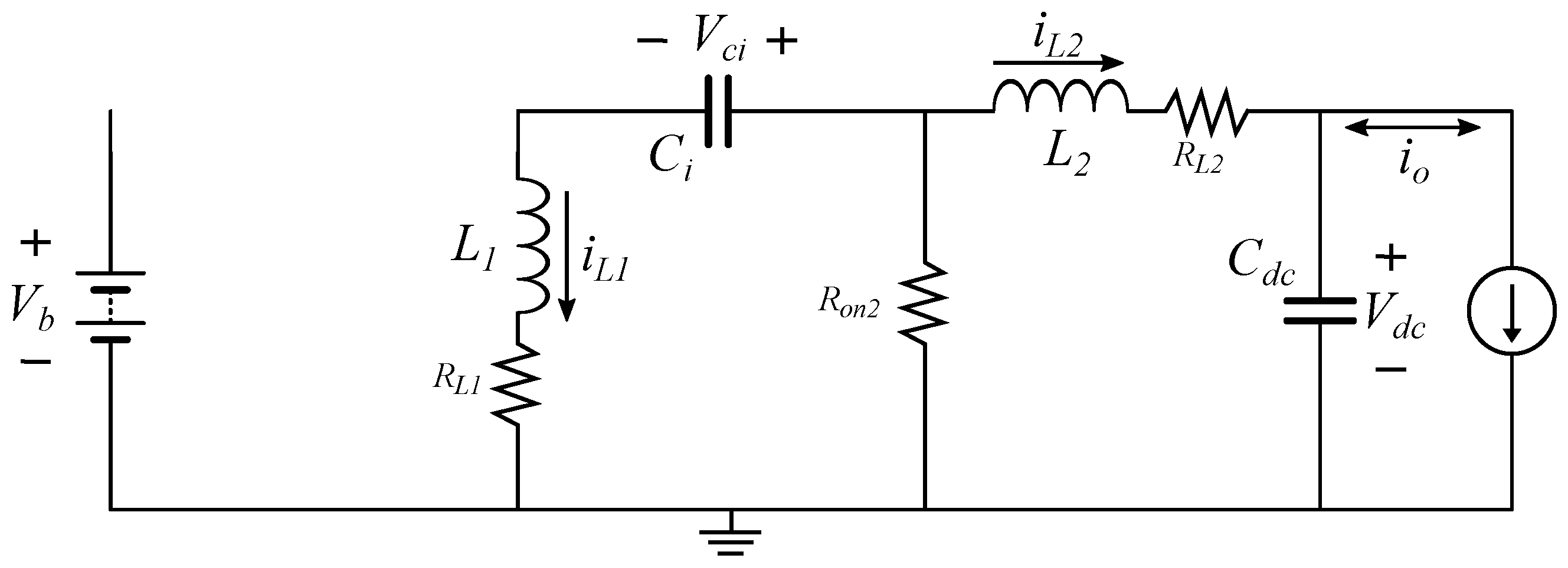
2.1. Circuital Interface

The battery charger/discharger is based on the bidirectional Sepic/Zeta topology, which is reported in Figure 1. Such a topology was selected to enable the connection of batteries with any voltage relation with the microgrid bus; thus, the battery charger/discharger could be used to connect any commercial battery to any microgrid bus. Figure 1 models the battery using a voltage source V b , while the dc bus (of the microgrid) is modeled using the bus capacitance C d c and the bus current i o . In such a dc bus model, the bus capacitance is formed by the output capacitances of the sources and the input capacitances of the loads connected to the bus. Similarly, the bus current is the result of the current balance in the bus, hence i o could be positive (the loads require a higher current than the current provided by the sources), negative (the loads require a lower current than the current provided by the sources), or zero (the loads require the same current provided by the sources). Finally, the charger/discharger must regulate the bus voltage V d c , which is needed to provide a safe operation condition to both sources and loads forming the microgrid.
The Sepic/Zeta bidirectional topology is formed by two MOSFETs ( M 1 and M 2 ) which are complementarily activated, two inductors L 1 and L 2 , and an intermediate capacitor C i . Finally, the circuital interface includes a PWM circuit to produce the complementary activation signals of the MOSFETs (u and u ¯ = 1 u ) from the desired duty cycle d.

2.2. Control-Oriented Model

This subsection provides a realistic control-oriented model of the circuital interface, which takes into account the parasitic resistances in both the MOSFETs and inductors as depicted in Figure 2.
The first step to develop a usable control-oriented model is to obtain the differential equations of both inductor currents and capacitor voltages for each possible state of the activation signal u. The circuit obtained from u = 1 is depicted in Figure 3, where the differential equations are:
d i L 1 d t = V b ( i L 1 + i L 2 ) · R o n 1 i L 1 · R L 1 L 1
d i L 2 d t = V c i ( i L 1 + i L 2 ) · R o n 1 + V b V d c i L 2 · R L 2 L 2
d V c i d t = i L 2 C i
d V d c d t = i L 2 i o C d c
Similarly, the circuit obtained from u = 0 is depicted in Figure 4, where the differential equations are:
d i L 1 d t = V c i ( i L 1 + i L 2 ) · R o n 2 i L 1 · R L 1 L 1
d i L 2 d t = V d c ( i L 1 + i L 2 ) · R o n 2 i L 2 · R L 2 L 2
d V c i d t = i L 1 C i
d V d c d t = i L 2 i o C d c
From the previous differential equations, the switched model is formed, which describes the dynamic behavior of the inductor currents and capacitor voltages depending on the activation signal u:
d i L 1 d t = ( V b ( i L 1 + i L 2 ) · R o n 1 ) · u + ( V c i ( i L 1 + i L 2 ) · R o n 2 ) · u ¯ i L 1 · R L 1 L 1
d i L 2 d t = ( V c i ( i L 1 + i L 2 ) · R o n 1 + V b ) · u ( i L 1 + i L 2 ) · R o n 2 u ¯ V d c i L 2 · R L 2 L 2
d V c i d t = i L 1 · u ¯ i L 2 · u C i
d V d c d t = i L 2 i o C d c
The previous model accurately describes the behavior of the bidirectional Sepic/Zeta structure, but this model does not includes the PWM circuit. Taking into account that the duty cycle corresponds to the averaged value of the activation signal u inside the switching period T s w , as given in (13), a new modeling approach including the PWM operation is obtained by averaging the switched differential equations within the switching period.
d = 1 T s w · 0 T s w u d t
Such an averaged model is obtained by replacing the binary signal u with the continuous duty cycle d. Taking into account that both MOSFETs supports the same current, the ON resistances of the MOSFETs are considered with the same value ( R o n 1 = R o n 2 = R o n ), which leads to the following averaged state-space system:
x ˙ 1 x ˙ 2 x ˙ 3 x ˙ 4 = R o n + R L 1 L 1 R o n L 1 ( 1 d ) L 1 0 R o n L 2 R o n + R L 2 L 2 d L 2 1 L 2 ( 1 d ) C i d C i 0 0 0 1 C d c 0 0 · x 1 x 2 x 3 x 4 + V b L 1 V b L 2 0 0 · d + 0 0 0 1 C d c · i o
y = 0 0 0 1 · x 1 x 2 x 3 x 4
where the states are:
x 1 = i L 1 x 2 = i L 2 x 3 = V c i x 4 = V d c
Figure 5 presents a comparison between the previous averaged nonlinear model and the circuital (switched) simulation performed in MATLAB. The magnitude and phase of the bode diagrams confirm the high accuracy provided by the averaged model in the reproduction of the circuit behavior. Moreover, the right side of the figure shows the dynamic response of both model and circuit to a step from d = 0.5 to d = 0.6 , where the main difference is the ripple oscillations present in the circuital (switched) simulation, which are not present in the averaged model. Therefore, for control-oriented purposes, the averaged model provides a satisfactory representation of the real circuit, including the parasitic losses.
In steady-state conditions, the derivatives of the state-space model are equal to zero, which leads to the steady-state conditions reported in (17)–(20); those equations consider equal the ON resistances of both MOSFETs, which is realistic since both MOSFETs support the same peak current.
V d c e = V b · d e 1 d e i o · R L 1 · d e 2 ( 1 d e ) 2 + R L 2 + R o n ( 1 d e ) 2
V c i e = V b · d e 1 d e i o · R L 1 · d e + R o n ( 1 d e ) 2
i L 1 e = i L 2 e · d e 1 d e
i L 2 e = i o
It is observed that the averaged model is a nonlinear system (14)–(16), thus it can be used to design linear controllers by obtaining the small-signal representation given in (21) and (22), where A m and B m are the matrices of (14) evaluated at the steady-state conditions, C m is the vector of (15), and D m = 0 . Finally, x ˜ , y ˜ and d ˜ are the small-signal changes on the state vector, output, and duty cycle, respectively.
x ˜ ˙ = R o n + R L 1 L 1 R o n L 1 ( 1 d e ) L 1 0 R o n L 2 R o n + R L 2 L 2 d e L 2 1 L 2 ( 1 d e ) C i d e C i 0 0 0 1 C d c 0 0 A m · x ˜ + V b + V c i e L 1 V b + V c i e L 2 i L 1 e i L 2 e C i 0 B m · d ˜
y ˜ = 0 0 0 1 C m · x ˜
where the states are:
x ˜ 1 = i ˜ L 1 x ˜ 2 = i ˜ L 2 x ˜ 3 = V ˜ c i x ˜ 4 = V ˜ d c

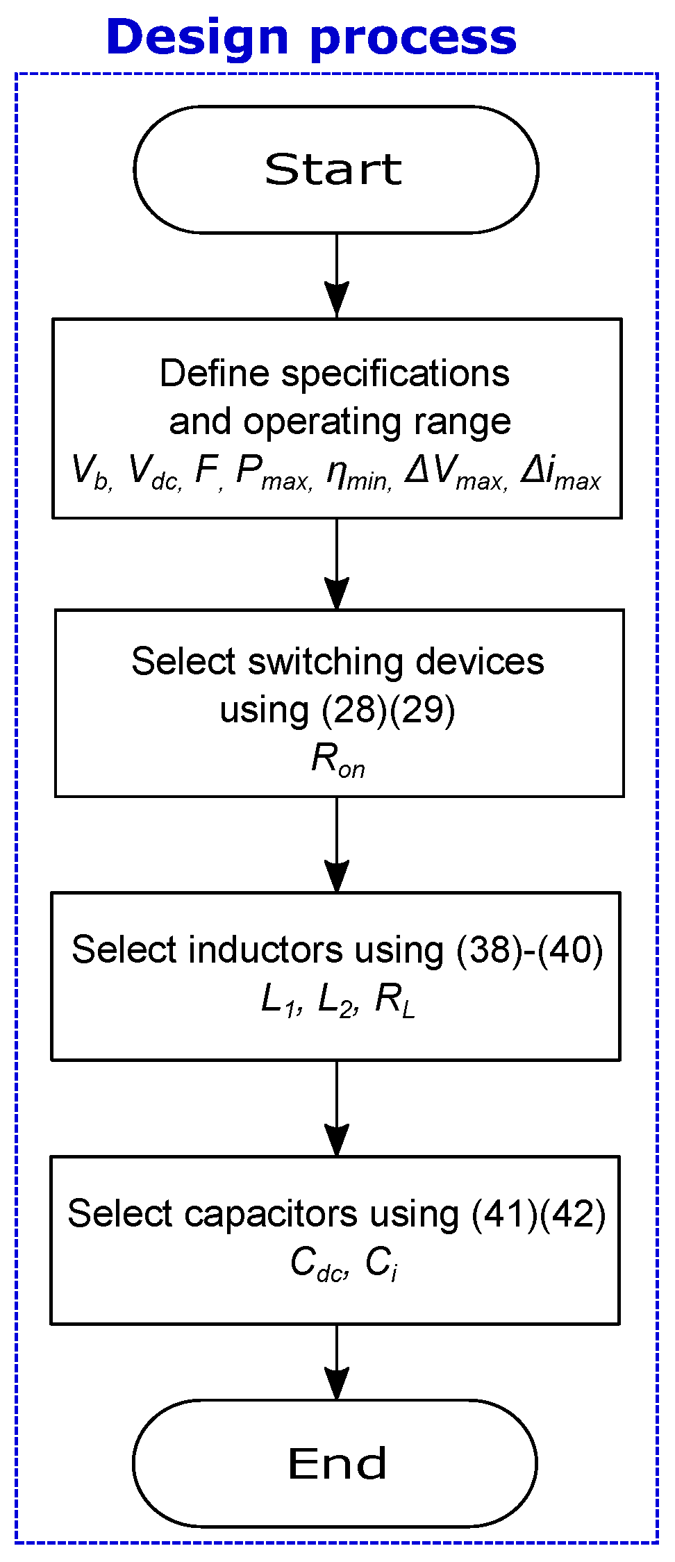
2.3. Design of the Power Stage

The design of the charger/discharger converter is performed based on the following criteria:
  • Range of dc bus voltage;
  • Maximum voltage ripple accepted in the dc bus;
  • Maximum power exchange with the dc bus;
  • Range of the battery voltage;
  • Maximum current ripple accepted in the converter inductors;
  • Minimum efficiency accepted for the charger/discharger.
From steady-state Equations (17)–(20), the averaged input current is calculated:
i i n t = ( i L 1 e + i L 2 e ) · d = d 1 d · i o
Then, the electrical efficiencies in discharge ( η d ) and charge ( η c ) conditions are calculated from Equations (17) and (23) as follows:
η d = 1 i o V b · R L 1 · d ( 1 d ) + R L 2 · ( 1 d ) d + R o n · 1 d · ( 1 d )
η c = 1 1 i o V b · R L 1 · d ( 1 d ) + R L 2 · ( 1 d ) d + R o n · 1 d · ( 1 d )
The previous equations relate the efficiency of the converter, the operation conditions, and the parasitic resistances in both inductors and MOSFETs. From those equations, it is observed that by increasing the bus current i o and operating with a bus voltage lower than the battery voltage, the converter efficiency is decreased. Therefore, the worst-case scenario for the converter efficiency is given in (26):
η d M i n = 1 i o M a x V b M i n · R L 1 · d ( 1 d ) + R L 2 · ( 1 d ) d + R o n · 1 d · ( 1 d )
Based on the previous equation, the maximum parasitic resistance allowed in the inductors is given in (27). Such an expression considers R L 1 = R L 2 , which is fair since both inductors support similar currents. In conclusion, the inductors must be selected with a maximum parasitic resistances R L M a x to ensure the desired efficiency is achieved.
R L M a x = ( 1 η r e q ) · V b M i n i o M a x R o n · 1 d · ( 1 d ) · d · ( 1 d ) 1 2 d + 2 d 2
The parasitic resistance of the MOSFETs R o n depend on the semiconductor characteristics. For this power interface, the maximum current and voltage that must be supported by both MOSFETs are given in (28) and (29), which are used to select the commercial MOSFETs for the charger/discharger, thus also helping to obtain the R o n value from the manufacturer’s datasheet.
i M m a x = i L 1 m a x + i L 2 m a x
V M m a x = V b m a x + V c i m a x
The peak values of the ripples in the inductor currents and capacitor voltages are obtained from differential Equations (1)–(4), respectively. Such a calculation is performed by applying the volt-second balance in the inductors and the charge balance in the capacitors [33]. Since the differential equations for i L 1 , i L 2 , and V c i are different in u = 0 and u = 1 , those ripples correspond to triangular waveforms, thus the peak values are calculated from (1)–(3) for the first section of the switching period, which has a duration of d · T s w : the peak ripple magnitude is calculated by multiplying the derivative of the state by d · T s w and dividing such a result by 2. On the other hand, the differential equations for V d c in u = 0 and u = 1 are equal, hence the ripple has a second-order waveform: in this case the voltage ripple is calculated by integrating the capacitor ripple ( Δ i L 2 i o ) within the complete switching period T s w = 1 / F , where F is the switching frequency. The resulting ripple equations are:
Δ i L 1 = ( V b ( i L 1 e + i L 2 e ) · R o n i L 1 e · R L 1 ) · d 2 · L 1 · F
Δ i L 2 = ( V c i e + V b V d c e ( i L 1 e + i L 2 e ) · R o n i L 2 e · R L 2 ) · d 2 · L 2 · F
Δ V c i = i o · d 2 · C i · F
Δ V d c = Δ i L 2 8 · F · C d c = ( V c i e + V b V d c e ( i L 1 e + i L 2 e ) · R o n i L 2 e · R L 2 ) · d 16 · C d c · L 2 · F 2
As in the efficiency criterion, the worst-case scenario is used to calculate the passive elements. From ripple Equations (30)–(33), it is observed that the parasitic resistances ( R o n , R L 1 , and R L 2 ) reduce the ripple magnitude, thus the worst-case scenario corresponds to a lossless device, which leads to the following minimum inductance and capacitance values:
L 1 M i n = V b M a x · d 2 · Δ i L 1 · F
L 2 M i n = V b M a x · d 2 · Δ i L 2 · F
C i M i n = i o · d 2 · Δ c i · F
C d c M i n = V b M a x · d 16 · Δ i L 2 · L 2 · F 2
Finally, the elements selection must include a safe margin to account for manufacturing tolerances. In this work, we adopted a 50% safe margin, but any other margin can be adopted:
L 1 > 1.5 · L 1 M i n
L 2 > 1.5 · L 2 M i n
R L < 0.9 · R L M a x
It must be noted that a large inductor could also exhibit large parasitic resistances, thus degrading the efficiency. Therefore, a proper balance must be found between inductance size and losses of the commercial devices. Then, using the selected inductances, the converter capacitances are selected using Equations (36) and (37) as follows:
C d c > 1.5 · C d c M i n
C i > 1.5 · C i M i n
Finally, Figure 6 summarizes the design process using a systematic flowchart.

3. Adaptive LQG Voltage Controller

The charger/discharger must regulate the bus voltage, which is needed to ensure the correct operation of the microgrid. Such a bus voltage regulation must be performed in any operation conditions, i.e., charge, discharge, and stand-by mode (null current exchange). Moreover, the controller must be stable in all the operation range, i.e., boosting and reducing voltage, hence the controller parameters must be adapted to the operation conditions. This process was performed by designing a linear quadratic Gaussian (LQG) controller with adaptive parameters. Therefore, three control blocks were designed: a linear quadratic integral (LQI) controller designed to regulate the bus voltage, an optimal observer to estimate the system states, and an adaptive law to adjust the LQI parameters depending on changes of the operation point.

3.1. LQI Controller Design
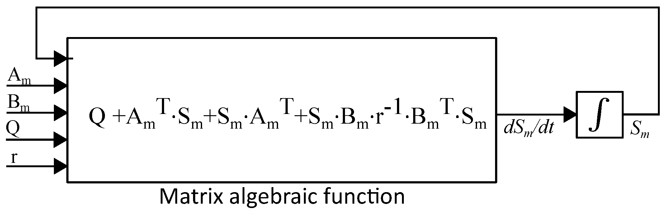
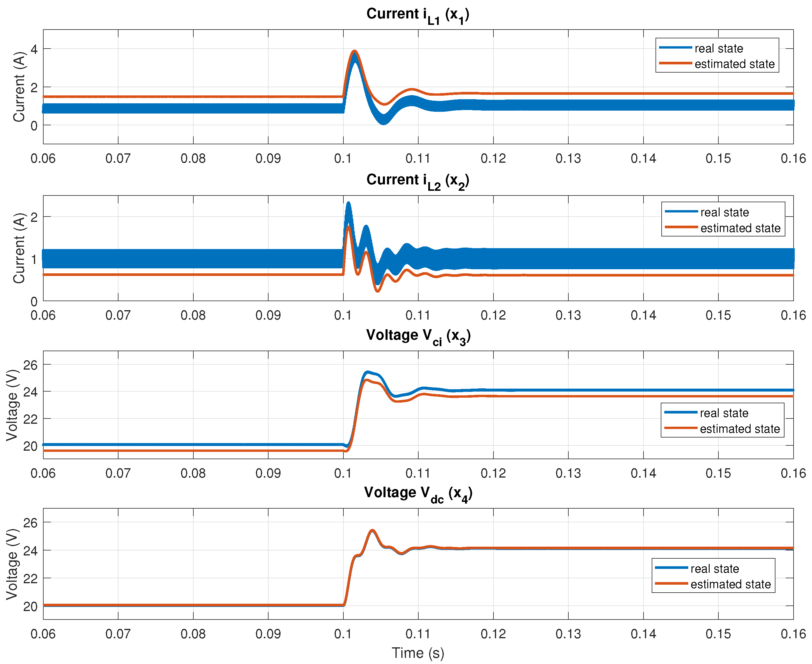
The bus voltage regulation is described as an optimal control problem, thus it is needed to define a cost function based on a quadratic expression, which is solved using the LQR paradigm [40]. However, in order to ensure a null steady-state error, the integral of the error is included into the system, which results in the problem known as LQI [41]. The formalization of the previous problem is as follows: find the optimal duty cycle value d ˜ ( t ) that minimizes expression (43).
J = 0 t f 1 2 · ( z ˜ T Q z + r d ˜ 2 ) · d t
The previous expression represents the quadratic cost functional from the initial time to the final time t f , where r is a positive scalar value and Q is a 5 × 5 positive matrix (size imposed by the states x ˜ defined in (16), plus the integral of the error):
Q = Q T > 0 r > 0
In addition, z ˜ is the extended state vector resulting from the inclusion of the error integral, named x ˜ i . Then, the state feedback law is imposed as given in (44), where K x is a gain vector that multiplies the states x ˜ , and K i is a scalar that multiplies the error integral.
d ˜ = K · z ˜ = K x K i · x ˜ x ˜ i
The inclusion of the error integral produces the following extended system, where C m has a negative sign due to the negative feedback of x ˜ 4 = V ˜ d c into the small-signal control system:
z ˜ ˙ = x ˜ ˙ x ˜ ˙ i = A m 0 C m 0 A w · x ˜ x ˜ i z + B m 0 B w · d ˜
Then, the optimization problem solution is calculated using the Hamiltonian matrix H ( z ˜ , d ˜ , P , t ) given in (46), where the state equations are reported in (47), the costate equations are given in (48), and the steady-state conditions are given in (49).
H ( z ˜ , d ˜ , P , t ) = 1 2 · ( z ˜ T · Q · z ˜ + r · d ˜ 2 ) + P T · ( A w · z ˜ + B w · d ˜ )
z ˜ ˙ ( t ) = A w · z ˜ + B w · d ˜
P ˙ ( t ) = Q · z ˜ + A w T · P
0 = r · d ˜ + B w T · P
In order to guarantee that the solution corresponds to the global optimal, the second-order optimality condition given in (50) must fulfilled:
2 H d 2 ( z ˜ , d ˜ , P , t ) = 2 · r > 0
Since r is defined as a positive value, H is a convex function, thus d ˜ corresponds to the minimum condition of H and it is the optimal solution around the operating point. The optimal value d ˜ is obtained from Equation (49) as follows:
d ˜ = r 1 · B w T · P
where P is defined as P = S m · z ˜
In the previous expression, S m is a 5 × 5 matrix, which is required to calculated the stage-feedback vector gain K, and it is discussed in Section 3.3. Replacing state-space Equation (47) into costate Equation (48), and considering that such an expression must be valid for all z conditions, the following restriction is obtained:
Q + A w T · S m + S m · A w S m · B w · r 1 · B w T · S m + S m ˙ = 0
The previous equation corresponds to the Riccati differential equation. Taking into account the control law defined in (51) and including the optimal duty cycle condition defined in (44), K is calculated as follows:
K = r 1 · B w T · S m
where S m is the solution of differential Equation (53). This problem is then formulated as an optimal regulator of infinite time, i.e., t f . In this case, the Riccati differential equation is solved backwards starting from t = t f , thus the initial condition is S m ( t f ) . The variable S m ( t ) has two components: a transient component and a steady-state one. Therefore, for t < < t f , the value of S m ( t ) corresponds to the steady-state solution of the Riccati equation S m e , which can be calculated by making the derivative S m ˙ ( t ) equal to zero in expression (53), which leads to:
S m e = lim t S m ( t )
Based on the previous solution, the controller is implemented using the following time-invariant feedback law:
d ˜ = r 1 · B w T · S m e · z ˜

3.2. State Observer

One of the main drawbacks of a feedback state controller is the requirement to measure all the states of the system; thus, several sensing circuits are required for the experimental implementation, which increases the implementation cost and complexity. This drawback is addressed for the proposed solution by designing a state observer, which only requires us to measure the dc bus voltage V d c .
The structure of the observer is presented in Figure 7, which corresponds to a full-state observer because all the states of the system are estimated. The inputs of the state observer are the measured voltage V d c and the duty cycle d, which are known. The output of the observer is the vector of estimated states, which are the inductor currents and capacitor voltages, as they were defined in Equation (16).
Considering the small-signal approximation of the system given in (21) and (22) and the feedback state law defined in (56) [42], the state observer is formalized as follows:
x ^ ˙ = A m · x ^ + B m · d · ( y y ^ ) = ( A m + · C m ) · x ^ + B m · d · y
y ^ = C m · x ^
where y corresponds to V d c as shown in Figure 7. Equation (57) shows that the observer gain vector defines the dynamic of the error estimation, such that the observer states converge to the states of the system. For determining , an optimization problem is defined to ensure the best estimation of the states are reached, and at the same time, the effect of the measurement noise in V d c is minimized. Similarly to the calculation of the feedback state vector K, the observer gain vector is determined in Equation (60), which requires to solve the Riccati differential equation given in Equation (59) [43]. In such an expression, S o corresponds to the optimal error covariance matrix of the state observer, and γ is a scalar to adjust the convergence speed of the observer states [44].
A m · S o + S o · A m T S o · C m T · γ 1 · C m · S o + B m · B m T + S o ˙ = 0
= S o · C m T · γ

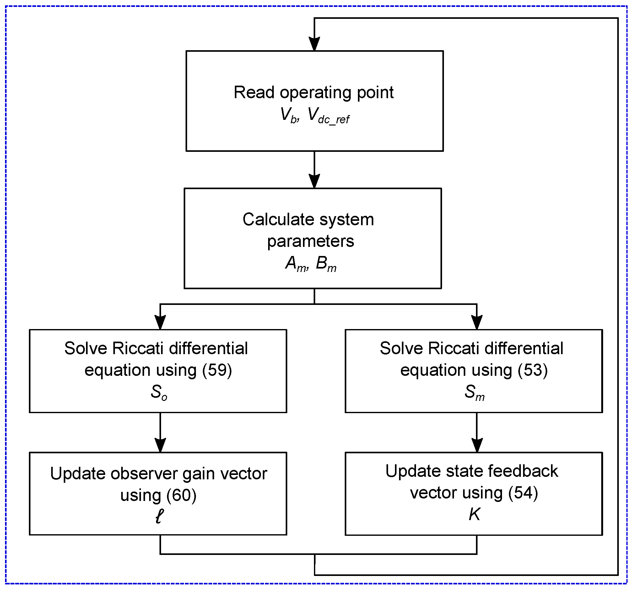
3.3. Adaptive Parameters of the LQI Controller

In order to guarantee a correct dynamic behavior of the charger/discharger in any operating conditions, an adaptive process to ensure the stability of the LQI controller is proposed. This means that the state feedback vector K is dynamically calculated depending on the operating condition. Such an adaptation is performed by continuously calculating the A m and B m matrices and continuously solving the Riccati differential equation.
The Riccati differential equation is solved online by the iterative procedure shown in Figure 8, which provides d S m d t . This value is integrated to obtain the matrix S m , which is used to determine the value of K from Equation (54). The same procedure is used to solve the differential Riccati equation given in (59), which provides S o to determine the observer state gain using expression (60). Both S m and S o matrices can exhibit positive and negative values; hence, those matrices are initialized with zeros to provide a homogeneous excursion of both positive and negative possibilities. This problem is defined as an infinite-time regulator, therefore the final S m and S o must be obtained in steady-state (derivates S m ˙ and S o ˙ equal to zero) for each operation point. The previous condition requires that the state observer calculations be performed fast, which is needed to ensure that the estimated states are available prior to the calculation of the optimal value d; such a procedure is discussed in Section 5. Finally, Figure 9 reports the procedure used to calculate the adaptive parameters of the LQI controller.

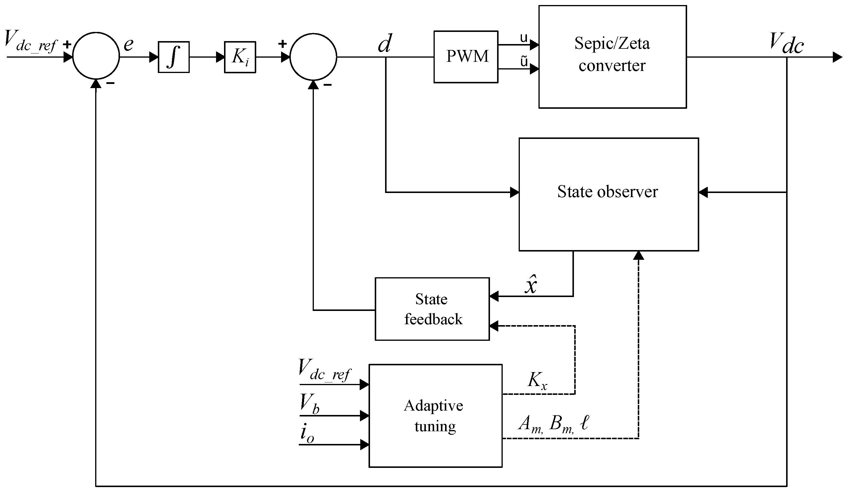
3.4. Structure of the Adaptive LQI Voltage Controller

The structure of the complete control system requires the interaction of the state observer, the state feedback (LQI) controller, and the adaptive tuning of the parameters. Such a structure is observed in Figure 10, where the LQI feedback is divided into the vector K x and the scalar K i , the last one processing the integral of the error. The adaptive tuning block produces the adaptive feedback vector K x and the matrices used to process the state observer ( A m , B m , ), which depend on the operating point defined by both the battery and the reference voltages. The real-time implementation of such a control system is described in Section 5.

4. Design Example and Simulation Results

This section illustrates the design process proposed in the flowchart of Figure 6 based on the realistic requirements reported in Table 1. This application case was defined to provide a realistic design, which is experimentally verified in Section 5. This proof-of-concept design considered a maximum battery power of 26 W, and the switching frequency F was chosen as 40 kHz due to the low requirements imposed to the PWM generator. The design example was developed in three phases: the calculation of the Sepic/Zeta converter parameters, the online calculation of the controller parameters, and the verification of the design using circuital simulations.
First, applying the design process of Figure 6, the commercial devices of Table 2 were selected.
Second, the controller parameters K and were calculated online following the procedure of Figure 9. Due to the low complexity implementation requirements, the Euler numerical integration method was selected to solve d S m d t .
Concerning the state penalty matrix Q and the control penalty scalar r [45], those parameters were determined using an iterative process to ensure a performance of the controlled system with a maximum overshoot of 10% and a stabilization time lower than 10 ms. Moreover, K i was defined as a constant because it did not depend on the operating point. The final values of the controller parameters were:
Q = 1 0 0 0 0 0 1 0 0 0 0 0 1 0 0 0 0 0 5 0 0 0 0 0 1 r = 1000 K i = 16
The designed battery charger/discharger was implemented in Simulink from Matlab [46] using the Simscape library and the Specialized Power Systems tools [47]. Such a library enabled us to model the power devices considering the parasitic resistances, voltage, and inductance of the diode, and the on-resistance of the transistor. In addition, the functions already built into Simulink were used to implement the proposed control scheme. The performance of the controlled system was tested for two goals: dc bus regulation and reference tracking, each one of them at different operating points.

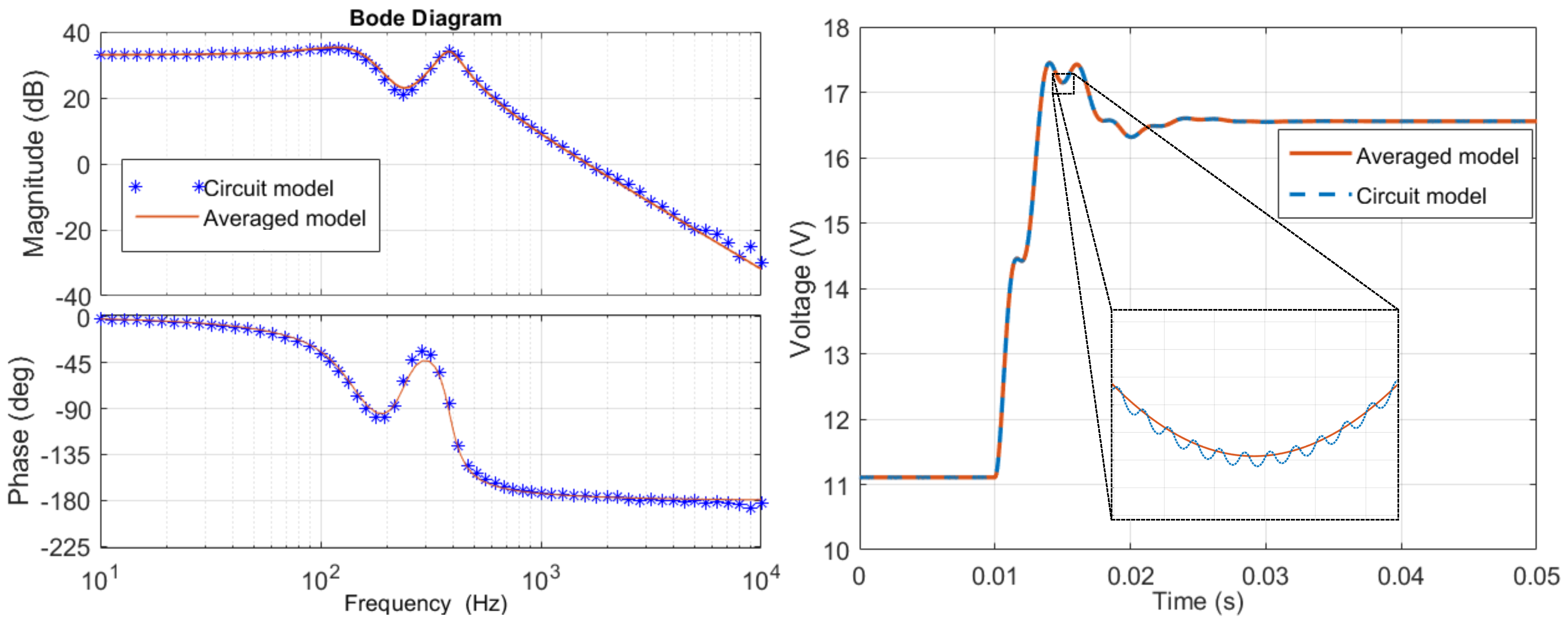
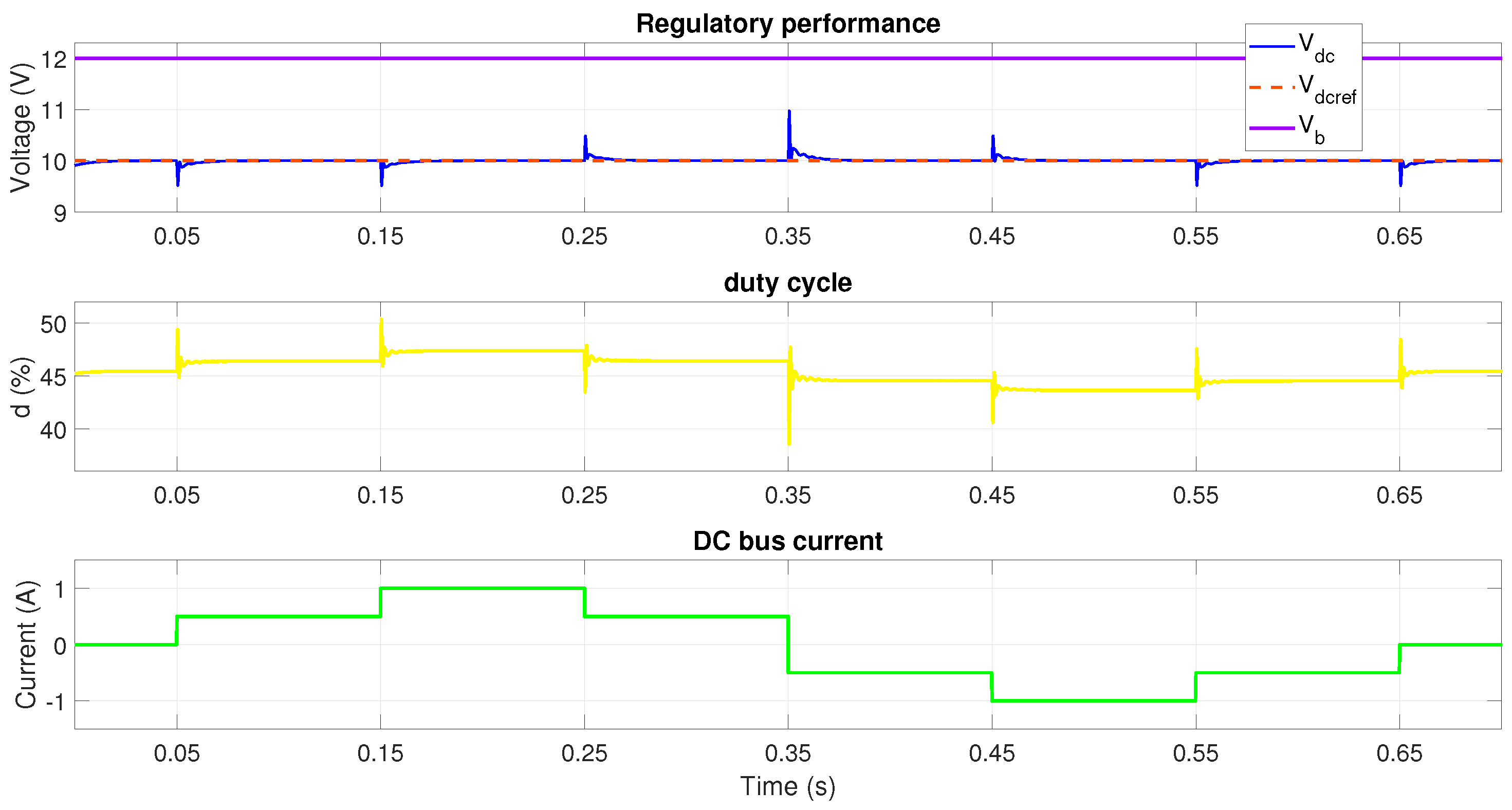
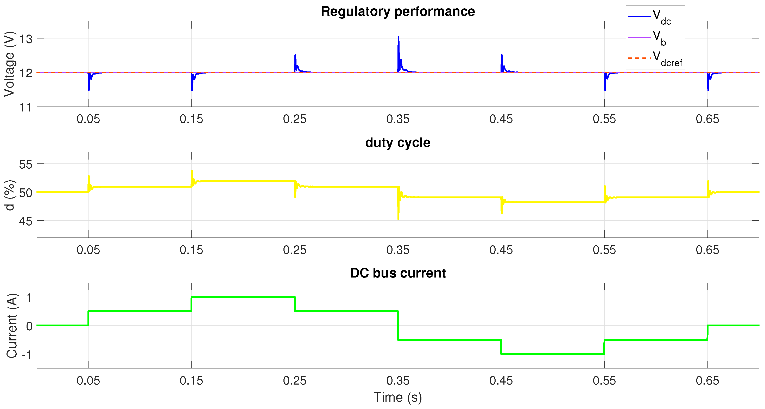
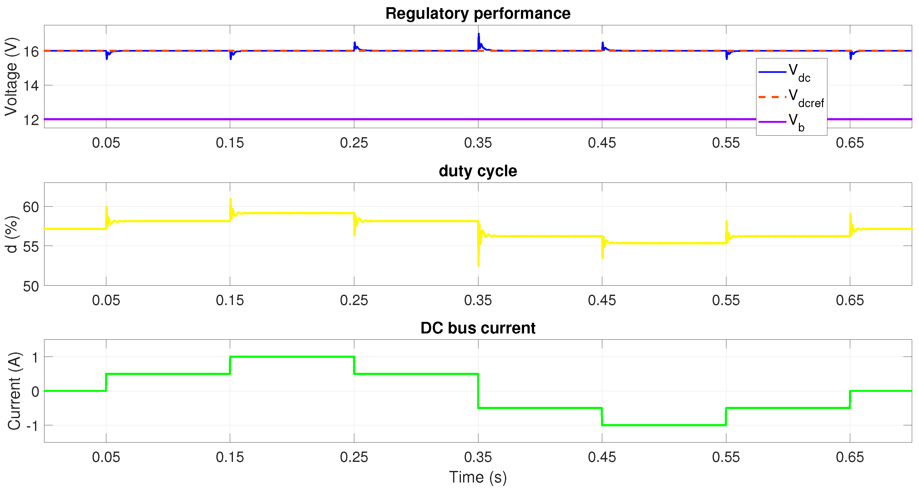
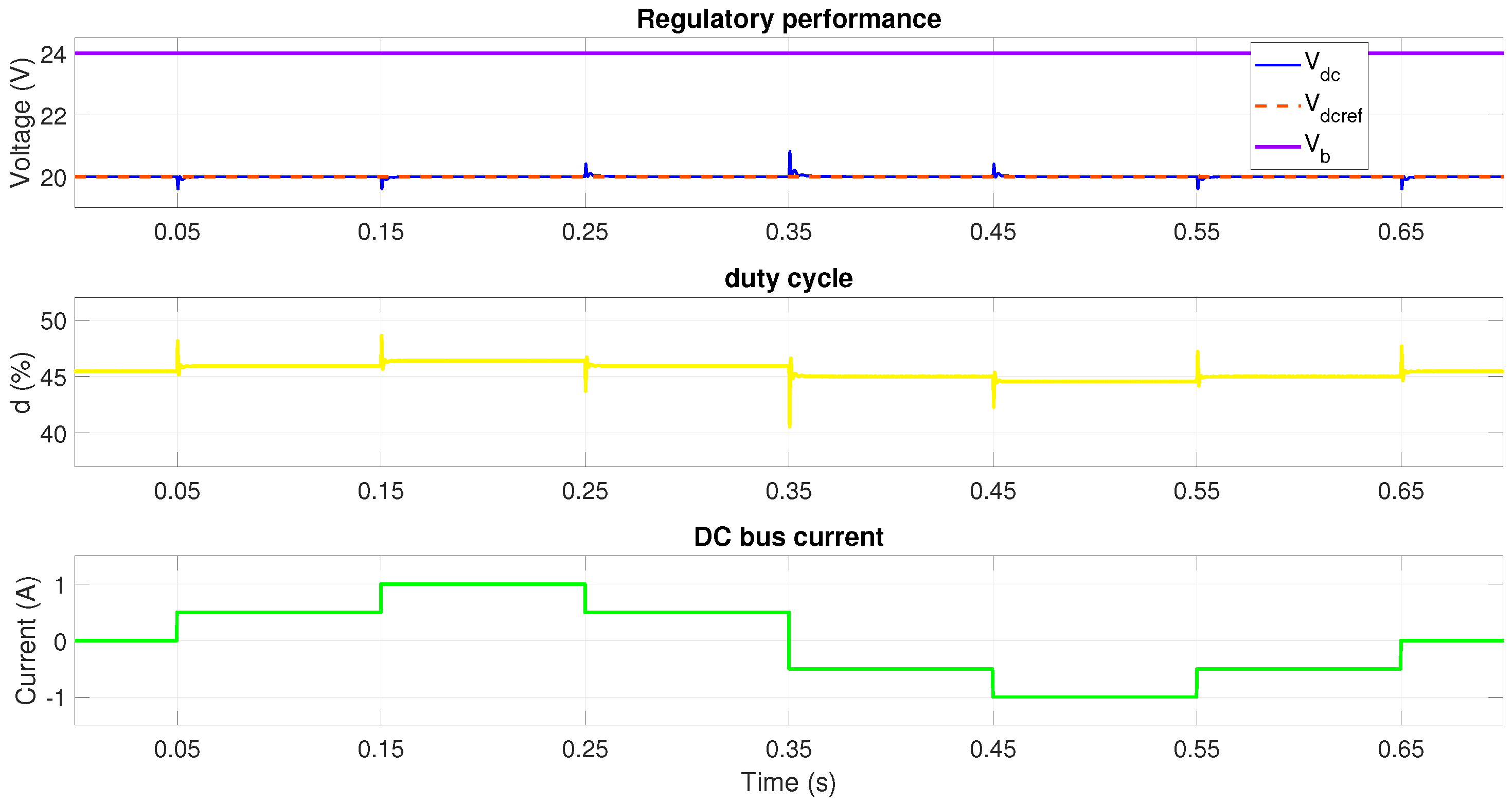
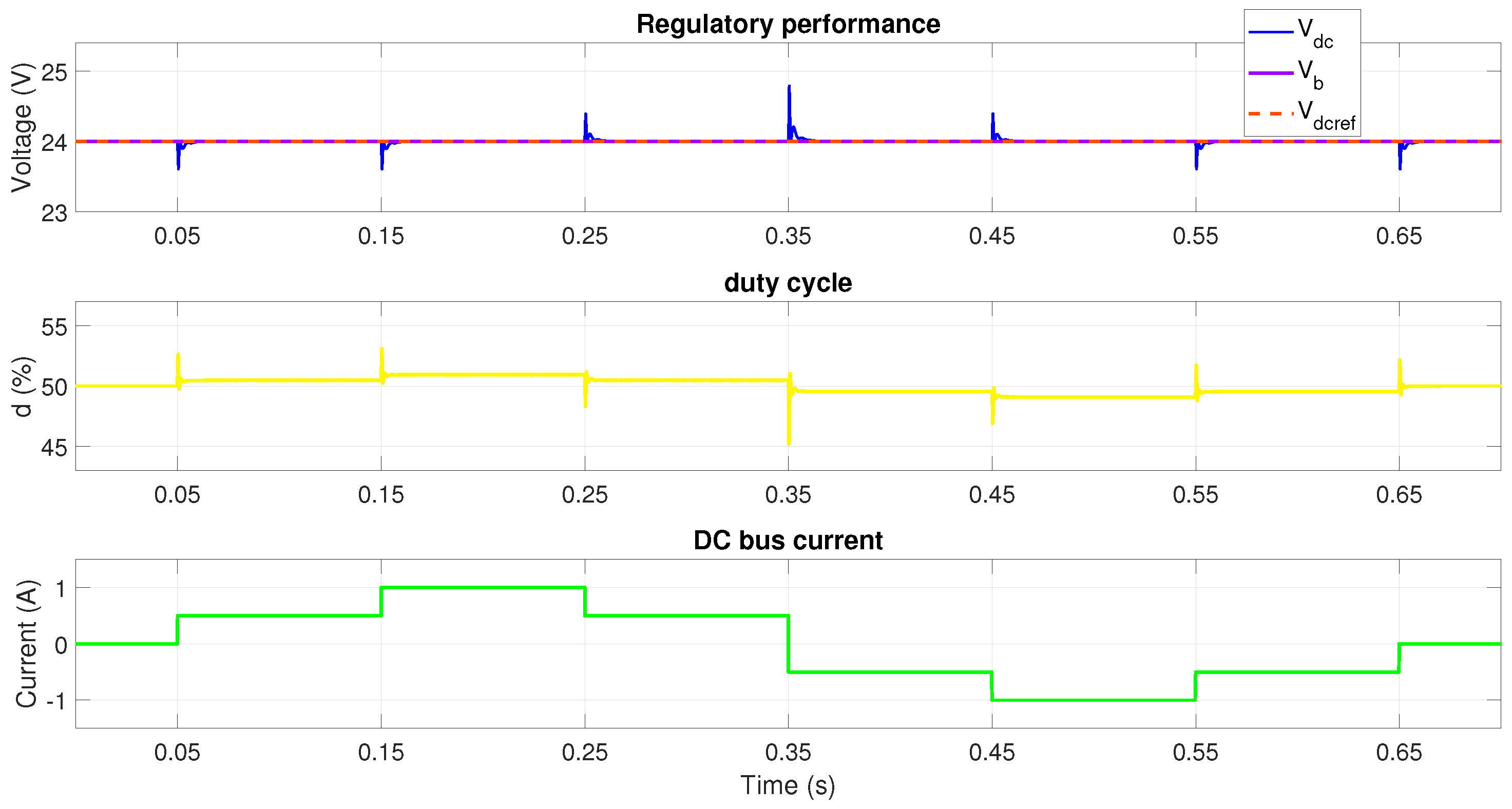
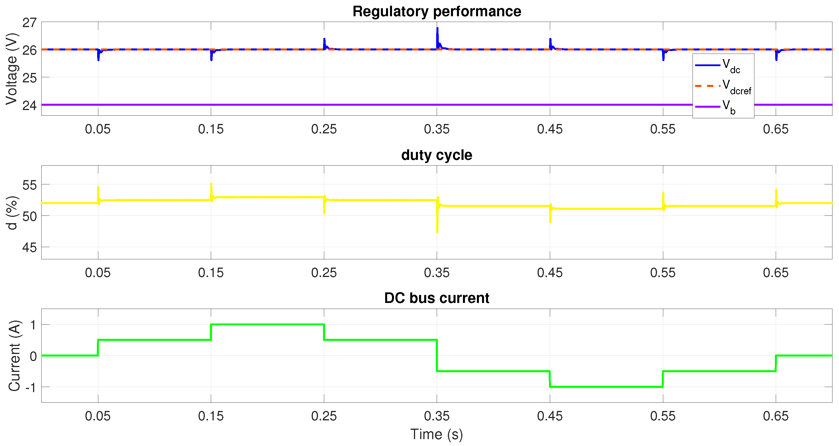
4.1. Simulations Results for Bus Voltage Regulation

The first objective was to regulate the bus voltage V d c under the presence of bus current disturbances ( i o ), which occurred due to changes of the power balance between the loads and sources of the microgrid. The microgrid bus current was defined to impose different operating modes to the battery, i.e., charge, discharge, and stand-by, all of them occurring in real situations. Moreover, some converter modes were also tested: buck (low bus voltage), boost (high bus voltage) and unitary gain.
Figure 11, Figure 12 and Figure 13 show the performance of the charger/discharger considering a 12 V battery. All the simulations started in stand-by mode, that is, i d c = 0 A . At 50 ms the bus current changed to 0.5 A, hence the battery entered the discharge mode ( i d c > 0 A ), and the battery had to supply the power required by the bus. At 150 ms and 250 ms, the bus current was increased to 1 A and decreased to 0.5 A, respectively. Then, at 350 ms, the bus current changed to −0.5 A, thus the battery entered the charge mode ( i d c < 0 A ), and the battery had to absorb the power excess present in the dc bus. An additional decrement of the bus current was applied at 450 ms, reaching a value of −1 A and returning to −0.5 A at 550 ms. Finally, at 650 ms, the battery reached the stand-by mode again. The same test was performed for bus voltages equal to 10 V (Figure 11, buck mode), 12 V (Figure 12, unitary gain mode), and 16 V (Figure 13, boost mode). The simulations confirmed the correct regulation of the bus voltage on any operation conditions of the battery, thus the bus voltage was stable under any microgrid conditions. Moreover, the controller adaptability was demonstrated since the change on the converter mode (buck, boost, unitary gain) was automatically compensated, hence it could be used to interface any commercial battery with any bus voltage level. Finally, the simulations also showed the duty cycle, which was never saturated, thus confirming the correct operation of both the observer and adaptive stage.
The same previous test was conducted while considering two batteries in a series connection, i.e., V b = 24 V , which enabled us to test the adaptability of the control system to changes on the battery voltage. The simulation results with such a new battery voltage are reported in Figure 14 (buck mode), Figure 15 (unitary gain mode), and Figure 16 (boost mode). In this case the bus voltage was set to 20, 24, and 26 V, respectively. As in the previous tests, the microgrid bus was successfully regulated for any operation conditions, and without any modification to the proposed control system.
Table 3 summarizes the performance of the charger/discharger under the different operating conditions and modes considered in this subsection. The results pointed out that the maximum overshoot was 9.7%, and the settling time was under 10 ms in all cases, hence the design requirements were fulfilled.

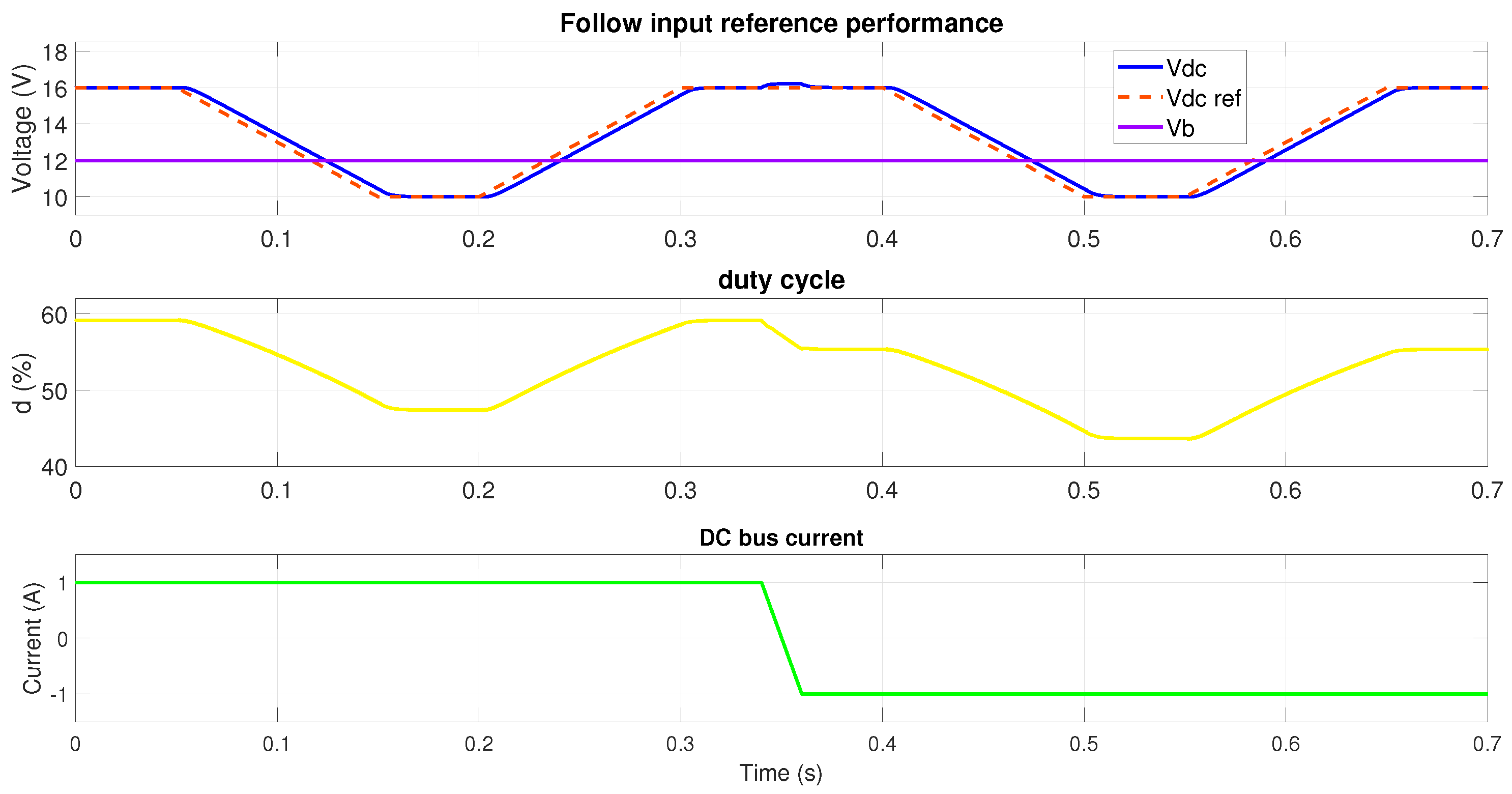
4.2. Simulations for Reference Tracking

Two simulation cases were conducted to evaluate the controller performance for reference tracking. In these tests, the bus voltage reference changed at 60 V/s around the battery voltage, which also forced the charger/discharger to enter in boost, buck, and unitary gain modes. Figure 17 shows the simulation results considering a battery voltage equal to 12 V, where the reference profile changed between V d c = 16 V and V d c = 10 V . In addition, the bus current changed from 1 A to −1 A, which set the battery in both charge and discharge modes. Therefore, the battery charger/discharger had to follow the reference profile when both charging and discharging the battery. As in the previous tests, the controller ensured the correct operation of the system, which in this case corresponded to a satisfactory reference tracking in any operation conditions.
The second test considered two batteries in a series connection, i.e., V b = 24 V . Those simulation results are reported in Figure 18, In this case, for evaluating the buck and boost modes of the converter, the reference changed between V d c = 20 V and V d c = 26 V , and the bus current set the battery in both charge and discharge modes. As in the previous case, the controller ensured a satisfactory tracking of the reference in any conditions.
The simulation results reported in Figure 17 and Figure 18 demonstrate the correct operation of the proposed solution under charge and discharges modes and reference tracking. The results showed a delay of 7 ms between the bus voltage change and the reference signal, which was lower than the settling time defined for the controller design (10 ms). Moreover, the simulations also confirmed that the control signal d was always far from the saturation limits. Therefore, the proposed adaptive controller ensured the global stability of the Sepic/Zeta converter in a large operation range and achieved the desired performance for any commercial battery and microgrid requirements.
Figure 19 reports the performance of the state observer under a step change on the reference at V b = 24 V . In this case, the duty cycle d changed by 10% around the steady state value (0.464), and the estimated states converged to conditions close to the real values. The results showed small steady-state errors, which did not significantly affect the controller performance as observed in both the simulations and experimental results of the complete system.

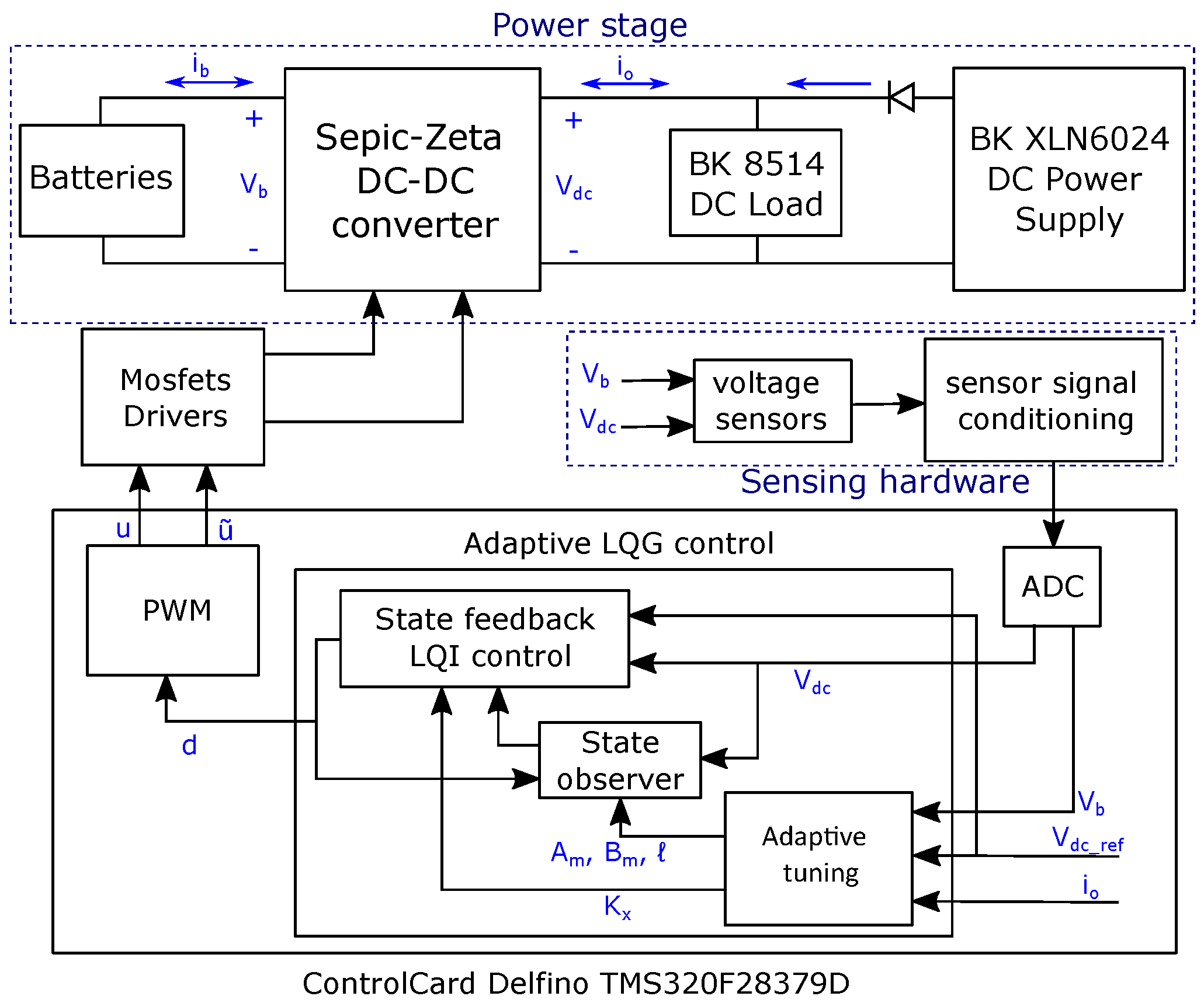
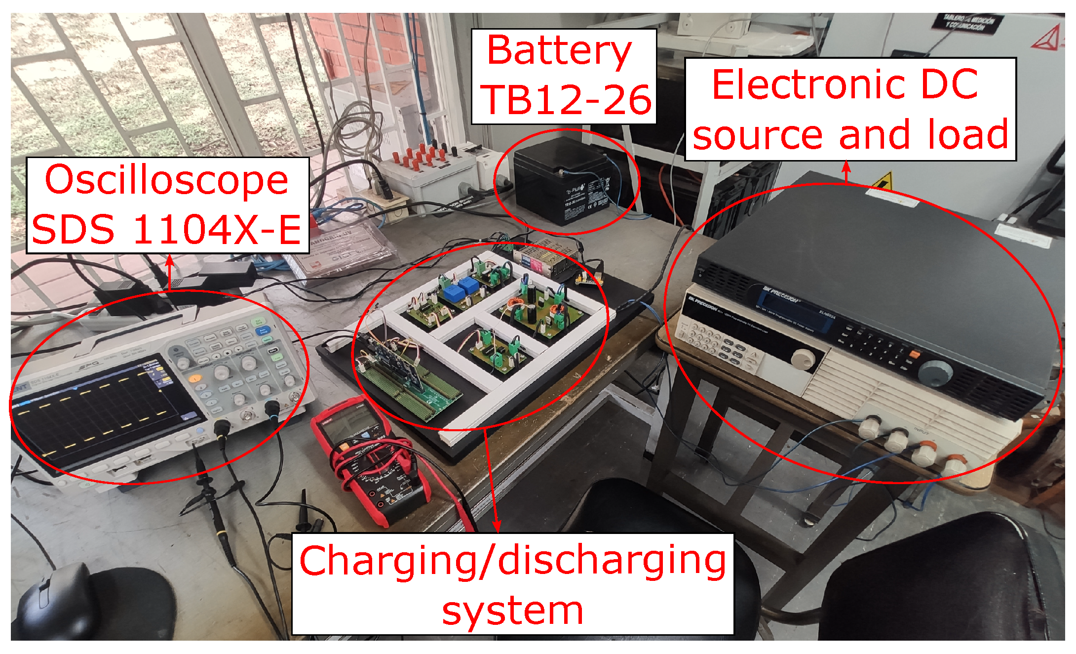
5. Experimental Validation

The battery charger/discharger designed in the previous section was experimentally implemented. Figure 20 shows the scheme of the test bench designed to validate the battery charger/discharger, which had the following blocks:
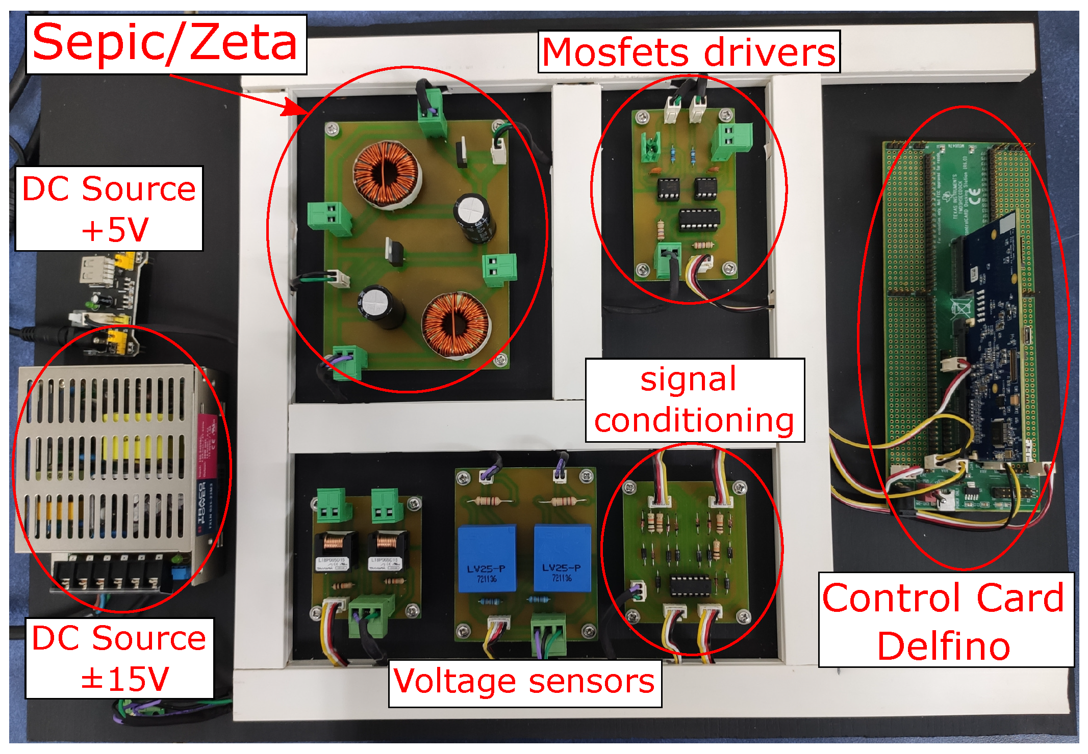
  • Power stage: it consisted of a 12 V battery, the bidirectional Sepic/Zeta converter, and the DC bus. A connection of the commercial electronic load (BK 8514) and the commercial source (BK XLN6024), using rectifier diodes in parallel to avoid reverse currents, was used to emulate a controllable dc bus.
  • Sensing hardware: LV25P voltage sensors were used to measure both the bus and battery voltages. The outputs of those sensors were isolated and scaled to the levels required by the control card.
  • Control card: the Texas Instruments Delfino TMS320F28379D control card was used to implement the adaptive controller and state observer. This control card has a 32-bit double core processor of the C2000 series at 200 MHz, four analog-to-digital converters (ADC), three 12-bit buffered digital-to-analog (DAC) outputs, 24 pulse width modulator (PWM) channels, input/output digital signals, among other features. In this experimental validation, a PWM module was used to generate the gate signals of the MOSFETs M1 and M2, also introducing the dead time required between both MOSFETs according to the datasheet. The control signal d was extracted from the control card using a DAC channel, for monitoring purposes, and the V d c and V b values were acquired using two ADC channels. In terms of software, the adaptive controller was implemented using the Embedded Coder Support Package for Texas Instruments C2000 Processor available in Matlab, which allowed us to generate C code from a Simulink model.
  • MOSFET drivers: two opto-coupled HCPL 3120 drivers were used to generate the isolated gate voltages for each MOSFET.
The experimental prototype is shown in Figure 21, where the power stage, sensors, and control card are observed. Figure 22 shows the complete experimental setup, which includes both the battery and the emulated microgrid bus. Such an experimental prototype was subjected to the same test conditions previously defined for the simulations, including multiple battery modes and converter operation conditions.

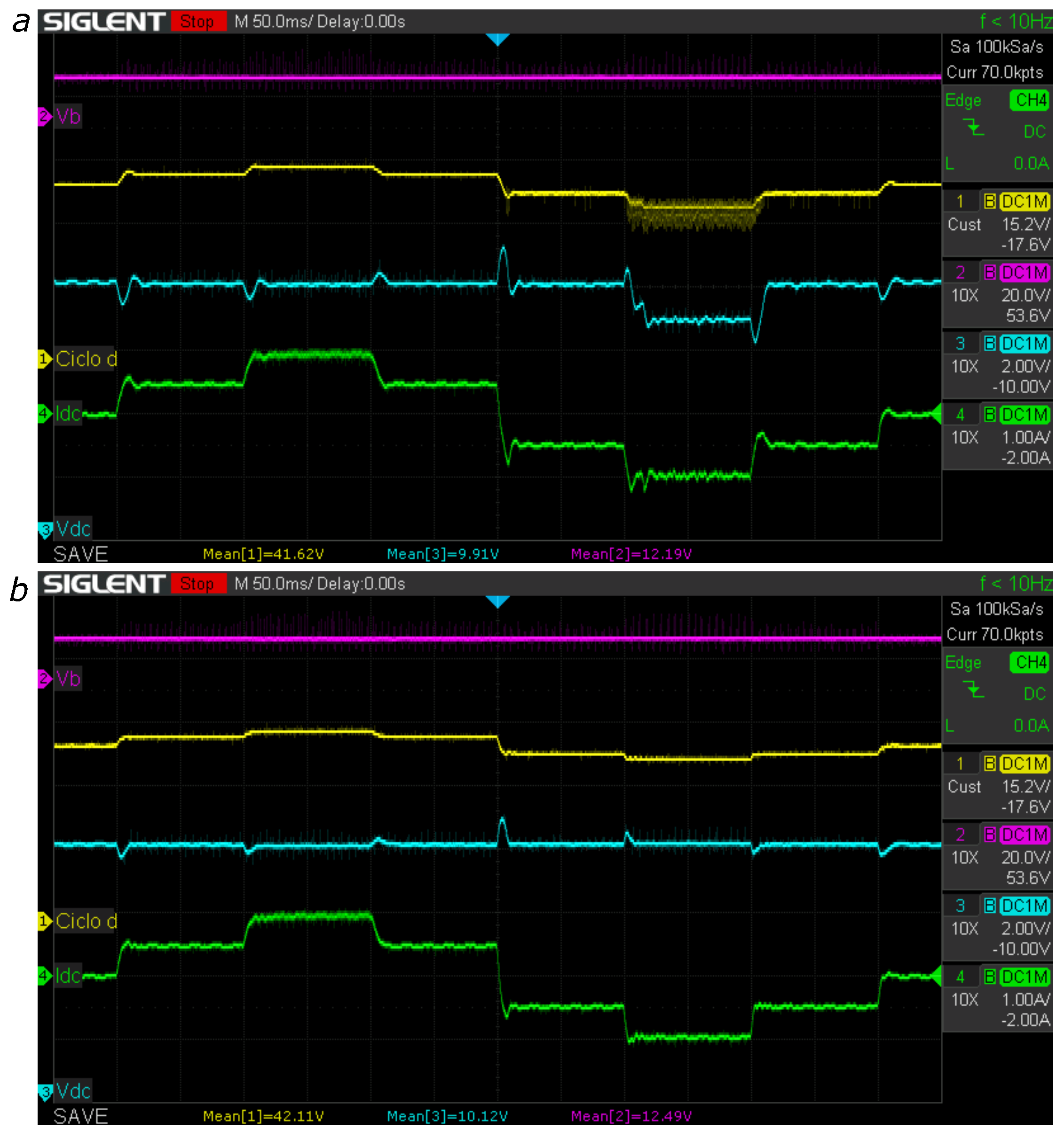
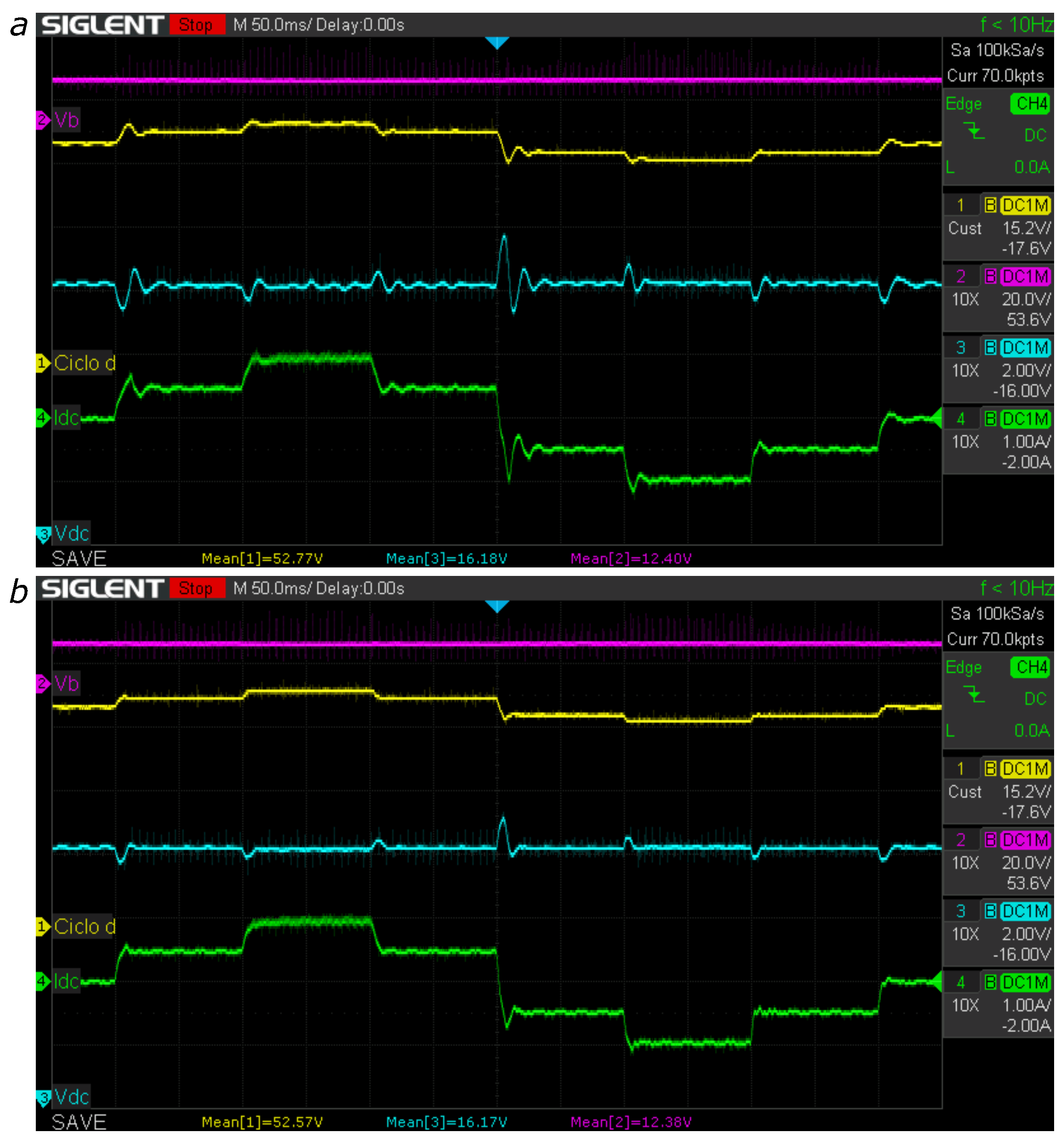
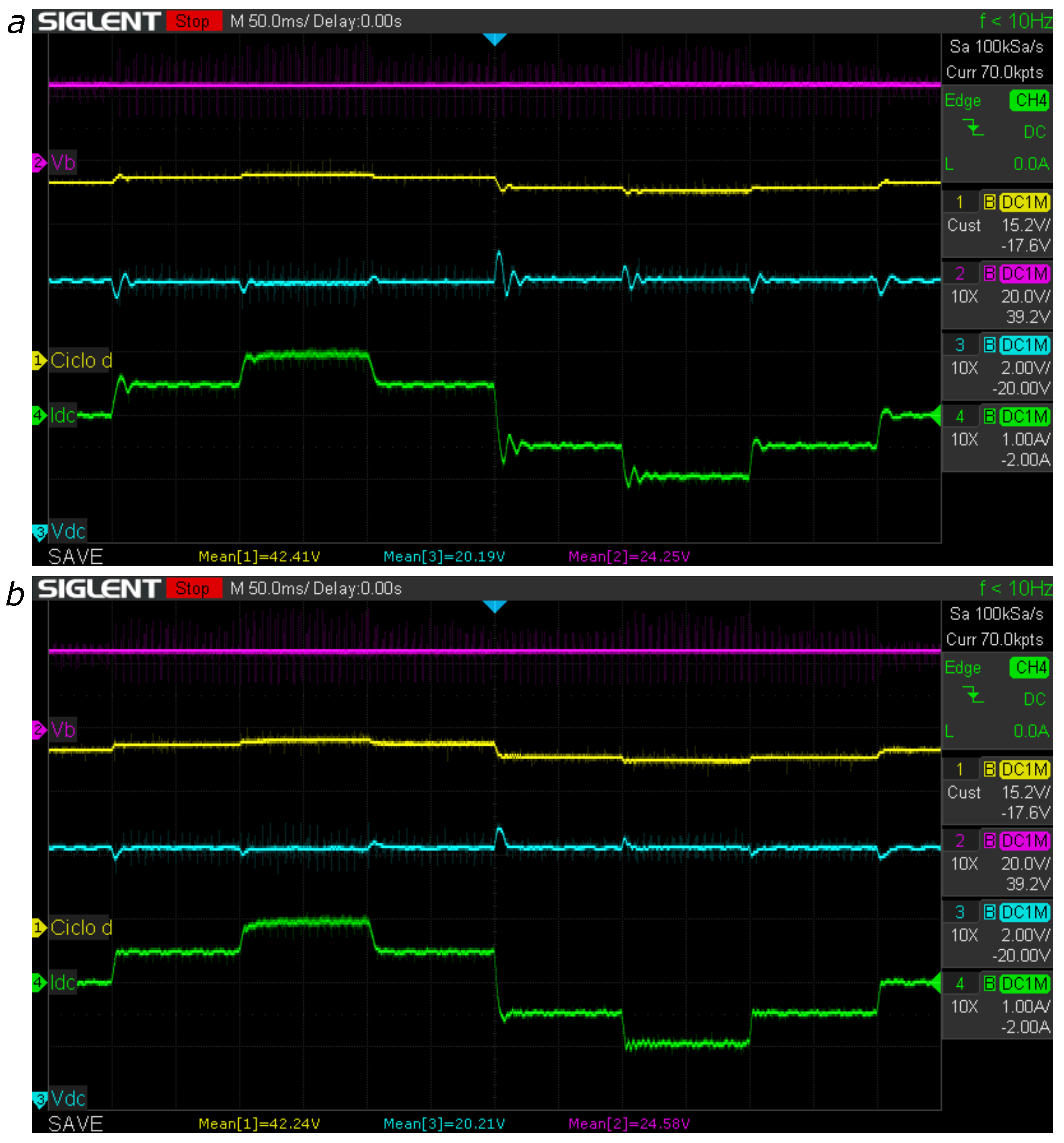
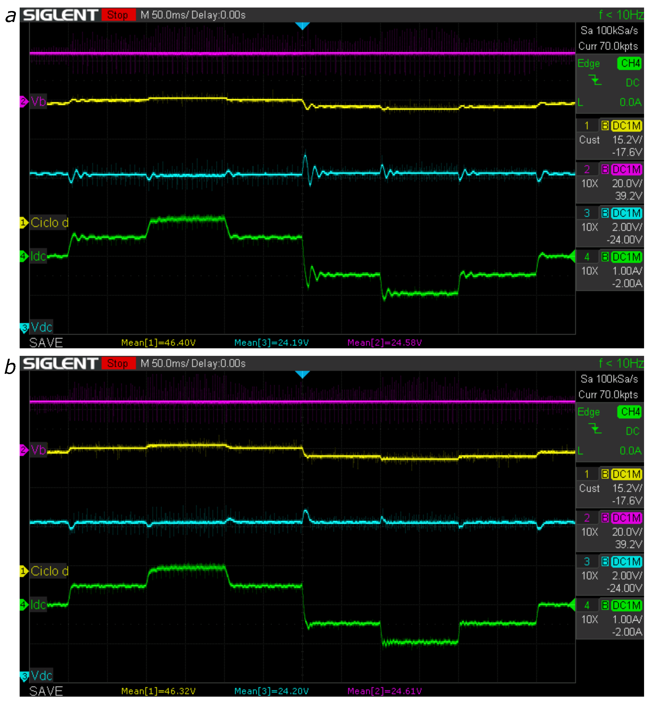
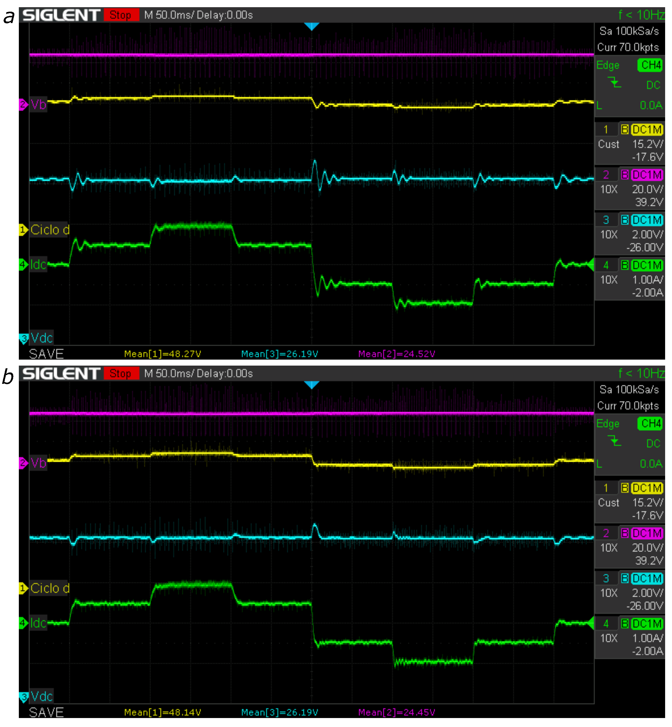
5.1. Experimental Results for Bus Voltage Regulation

The experimental validation of the proposed control system also considered the comparison with a classical solution, i.e., a proportional–integral (PI) control law, which illustrated the adaptability of the new solution. The PI controller was designed at the operating point ( V b = 12 V and V d c = 16 V ) using the pole placement technique. Figure 23a shows the performance of the charger/discharger under the action of the PI controller, where the bus voltage was regulated at 10 V (buck mode) for charging, discharging, and stand-by mode. The experiment considered bus currents of −1.0 A, −0.5 A, 0.0 A, 0.5 A and 1.0 A with step changes, which was the same bus current profile considered in the simulations. The experiment showed that the PI controller was unable to regulate the bus voltage for the deep charging condition of −1.0 A, which was caused by the large deviation from the operating point used to design the PI controller. In contrast, Figure 23b shows the experimental performance of the charger/discharge under the action of the proposed adaptive controller, where the bus voltage was successfully regulated for all the operation conditions. Moreover, the adaptive LQI controller provided a much stable bus voltage, also exhibiting smaller overshoots and shorter settling times.
The same previous test was performed for unitary gain (12 V) and boost (16 V) modes to validate the controller capability to adapt to different bus voltages without any modification. The results of those experiments are reported in Figure 24 and Figure 25, which put into evidence the satisfactory performance of the proposed solution (Figure 24b and Figure 25b). In addition, those results also show the improved performance of the adaptive LQI controller over the classical PI controller in all operation conditions: the new solution provided smaller overshoots and shorter settling times.
The next set of experiments were aimed at validating the capability of adapting to changes on the battery voltage without any modification. Those experiments considered two batteries in a series connection, thus increasing V b to 24 V. The experiments considered the same bus current profile used in the previous tests, which forced the battery pack to operate in charge, discharge, and stand-by modes. Figure 26, Figure 27 and Figure 28 reports the experimental results for bus voltages equal to 20 V (buck mode), 24 V (unitary gain mode), and 26 V (boost mode), respectively. The satisfactory performance of the proposed controller confirmed the adaptability of the new solution to changes on both the battery and the bus voltages, even under different operation modes of the battery. In addition, the experimental behavior of the proposed battery charger/discharger for a single battery (12 V) or a two-battery pack (24 V) put into evidence the improved performance over the classical PI solution. Moreover, all the experiments confirmed the correct duty cycle operation, which was never saturated.
Table 4 summarizes the experimental performance of the proposed solution and the classical PI controller. The data confirmed that the adaptive LQI controller always provided a maximum overshoot lower than 10% and settling times shorter than 10 ms, thus fulfilling the design criteria. On the contrary, the PI controller exhibited poor performance in the majority of the tests, where a maximum overshoot of 12% was observed, and longer settling times were also provided. Moreover, the proposed controller regulated the bus voltage in all the operation conditions, which was not ensured by the PI controller: for example, the PI controller was unable to regulate the bus voltage in charge mode with a bus current of 1 A (see Figure 23a), where the bus voltage had a steady-state error higher than 10%.
Although the simulation and experimental tests were performed for the same conditions, the experimental performance of the adaptive LQI controller exhibited some differences as observed in Table 3 and Table 4. Those differences were caused by nonmodeled parasitic effects on the wires, the internal resistances of the capacitors, parasitic inductances and capacitances on the MOSFETs, among other sources. However, both simulated and experimental implementations of the proposed solution fulfilled the designed criteria, which confirmed the viability of the solution for commercial applications.

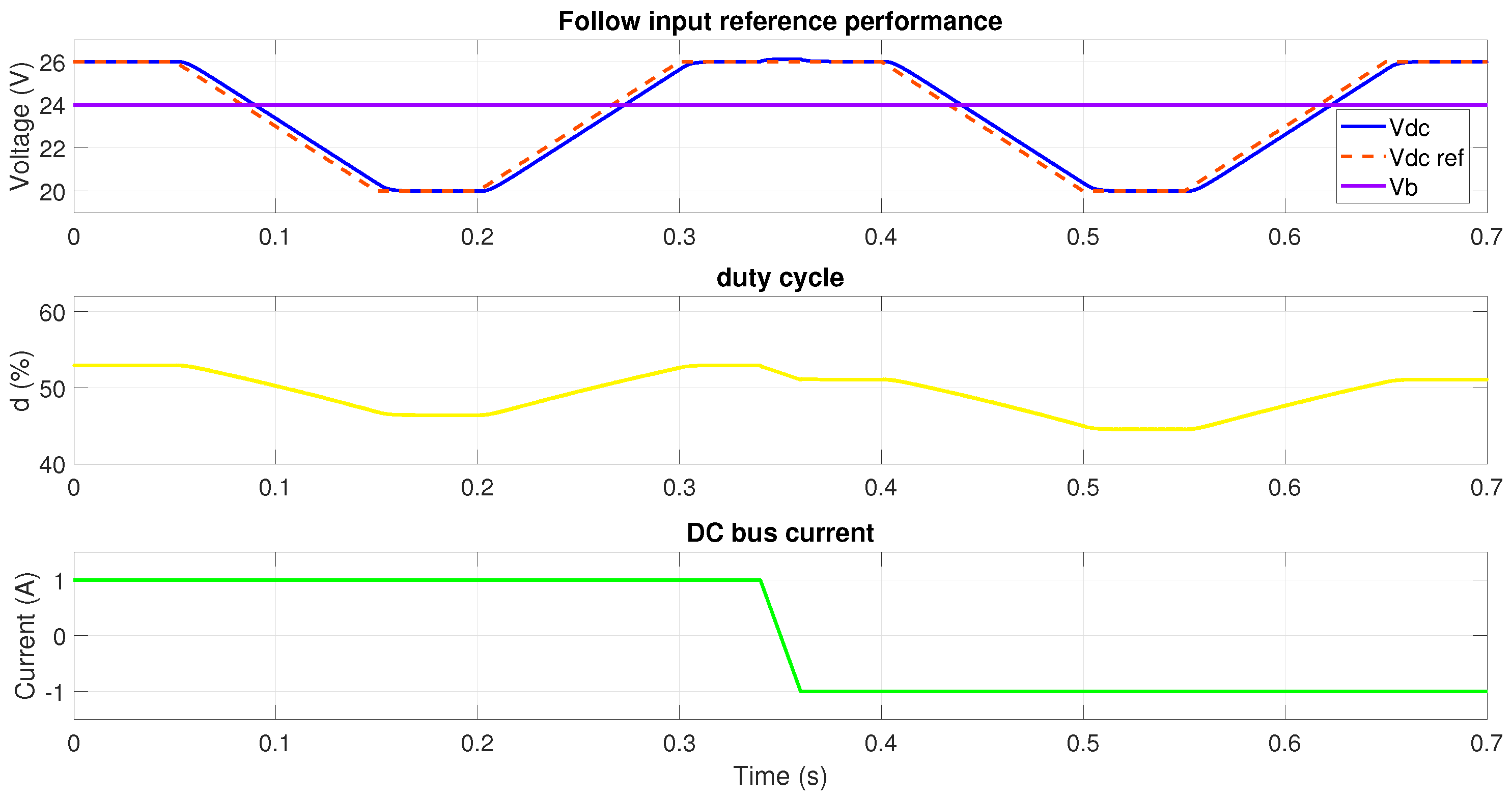
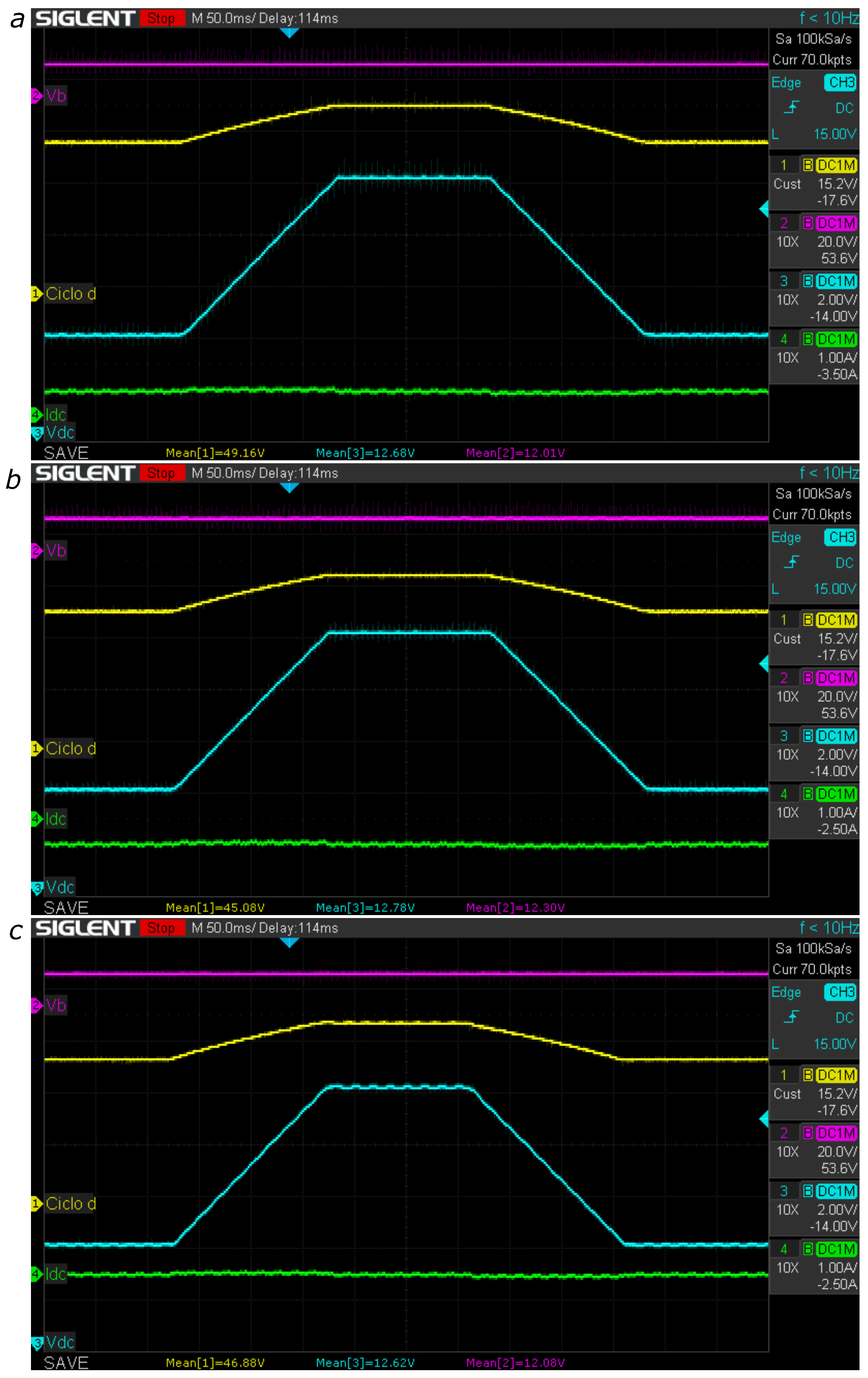
5.2. Experimental Results for Reference Tracking

The final set of experiments was conducted to verify the performance of the proposed solution in tracking a changing reference. These new experiments considered a particular battery mode (charge, discharge, stand-by) and applied a change on the bus voltage reference to force the converter into buck and boost modes, all of them for a single battery voltage V b = 12 V. The results of the experiments are reported in Figure 29, where the battery charger/discharger started operating with a bus voltage of 10 V (buck mode), changing to 16 V (boost mode), and returning to the buck mode again. As in the previous experimental tests, the proposed adaptive controller ensured a correct regulation of the bus voltage under any operation conditions. Moreover, the duty cycle was never saturated, which ensured the system controllability.
Finally, the experimental tests presented in this section demonstrated the following conditions:
  • The proposed adaptive LQI controller was able to adjust the parameters to ensure global stability and the desired performance under any operation conditions of the battery (charge, discharge, stand-by) and the converter (buck, boost, unitary gain).
  • The experiments and simulation fulfilled the design criteria, hence the design procedure proposed in this paper was correct. Moreover, this also confirmed the validity of the mathematical model developed for control purposes.
  • It was possible to implement the proposed adaptive LQI controller using commercial devices, which ensured the commercial viability of the proposed solution.
  • The proposed controller provided a better performance in comparison with classical solutions such as PI controllers, which were not able to ensure global stability.

6. Conclusions

In this work, a battery charger/discharger able to regulate the bus voltage under different operation conditions and perturbations was presented. The charger/discharger was based on the bidirectional Sepic/Zeta topology to enable the interaction of microgrid buses and battery packs with any voltage. The proposed mathematical model and design process included the main parasitic losses, thus providing a high accuracy and effectiveness.
The designed LQI adaptive control included a state observer to avoid many sensors, and it was designed to ensure a zero steady-state error and the system stability over a large operating range. Moreover, the adaptive controller guaranteed the desired performance of the charger/discharger in different battery and converter modes; thus, the proposed solution was able to operate under different gain relations among bus voltage and battery voltage, hence it was suitable to produce a general battery interface for any commercial storage and microgrid devices.
The core of the designed system was a set of matrix algebraic operations and integrators, which were used to implement the proposed adaptive controller. This solution was demonstrated to be suitable for implementation in many processing platforms such as DSPs, FPGAs, microcontrollers, among others. Such a condition was verified using an experimental implementation, which implemented the power stage using commercial hardware, and the control system was implemented using a commercial microprocessor. The experiments conducted verified the accuracy of the design procedure, where the main design criteria were fulfilled (maximum overshoot and settling time). Moreover, the experiments also confirmed the advantages over classical linear controllers: both global stability and desired performance were achieved in any operation conditions (charge, discharge, and stand-by modes of the battery; and buck, boost, and unitary gain modes of the converter). Therefore, the proposed solution is suitable to interface any battery pack with any microgrid. In fact, it is useful to replace series-connected battery packs with single batteries, since the boosting factor of the Sepic/Zeta converter will remove the need of a battery-balancing system commonly required in a series connection. In addition, such a modification will allow one to hot-swap any battery from the microgrid, thus reducing the maintenance stops.
In this implementation, the adaptive tuning was performed considering the worst case for the output current i o ; thus, it was introduced as a constant. However, i o could be measured rather than inserted as a constant (worst-case) value. This is a future improvement which will require to add a current sensor, thus increasing the system complexity.
In addition, the delay in reference tracking can be reduced by modifying the dynamic criteria adopted for the controller design, in particular reducing the settling time of the bus voltage. However, it must be taken into account that reducing the settling time also could increase the maximum overshoot, which could lead to undesired (or even dangerous) overvoltage conditions in the dc bus. Therefore, the complete dynamic performance must be analyzed.
Finally, an additional future work concerns the inclusion of the battery charging/discharging profile into the control system, which could be operated in agreement with the secondary control loops of the microgrid.

Author Contributions

Conceptualization, J.A.M.-O., C.A.R.-P., M.L.O.-G., E.F.-M. and S.I.S.-G.; methodology, J.A.M.-O., C.A.R.-P., M.L.O.-G., E.F.-M. and S.I.S.-G.; software, J.A.M.-O., C.A.R.-P., M.L.O.-G., E.F.-M. and S.I.S.-G.; validation, J.A.M.-O., C.A.R.-P., M.L.O.-G., E.F.-M. and S.I.S.-G.; writing—original draft preparation, J.A.M.-O., C.A.R.-P., M.L.O.-G., E.F.-M. and S.I.S.-G.; writing—review and editing, J.A.M.-O., C.A.R.-P., M.L.O.-G., E.F.-M. and S.I.S.-G. All authors have read and agreed to the published version of the manuscript.

Funding

This research was funded by Minciencias, Universidad del Valle, Universidad Nacional de Colombia, and Instituto Tecnológico Metropolitano under the research project “Métodos y Herramientas para el Diseño, Dimensionamiento y Control de Sistemas de Almacenamiento de Energía en sistemas eléctricos basados en fuentes renovables no convencionales, para zonas urbanas y rurales”, (Minciencias code 70634, Sicop Code C.I. 21154), which belongs to the research program “Estrategias para el desarrollo de sistemas energéticos sostenibles, confiables, eficientes y accesibles para el futuro de Colombia”, (Minciencias code 1150-852-70378, Hermes code 46771, Sicop codes C.I. 21154, 21173, 21174, ITM code RC 80740-178-2021-1).

Data Availability Statement

The data used in this study are reported in the paper figures and tables.

Conflicts of Interest

The authors declare no conflict of interest.

References

  1. Bandara, G.; Rajakaruna, S.; Ghosh, A. Evaluating of Frequency Response Time Characteristics of Large Scale Energy Storage Systems in High Renewable Energy Penetrated Power Systems. In Proceedings of the 2021 31st Australasian Universities Power Engineering Conference (AUPEC), Perth, Australia, 26–30 September 2021; pp. 1–6. [Google Scholar] [CrossRef]
  2. Lawder, M.T.; Suthar, B.; Northrop, P.W.C.; De, S.; Hoff, C.M.; Leitermann, O.; Crow, M.L.; Santhanagopalan, S.; Subramanian, V.R. Battery Energy Storage System (BESS) and Battery Management System (BMS) for Grid-Scale Applications. Proc. IEEE 2014, 102, 1014–1030. [Google Scholar] [CrossRef]
  3. Evans, A.; Strezov, V.; Evans, T.J. Assessment of utility energy storage options for increased renewable energy penetration. Renew. Sustain. Energy Rev. 2012, 16, 4141–4147. [Google Scholar] [CrossRef]
  4. Divya, K.; Østergaard, J. Battery energy storage technology for power systems—An overview. Electr. Power Syst. Res. 2009, 79, 511–520. [Google Scholar] [CrossRef]
  5. Rey, J.M.; Vera, G.A.; Acevedo-Rueda, P.; Solano, J.; Mantilla, M.A.; Llanos, J.; Sáez, D. A Review of Microgrids in Latin America: Laboratories and Test Systems. IEEE Lat. Am. Trans. 2022, 20, 1000–1011. [Google Scholar] [CrossRef]
  6. Zarate-Perez, E.; Rosales-Asensio, E.; González-Martínez, A.; de Simón-Martín, M.; Colmenar-Santos, A. Battery energy storage performance in microgrids: A scientific mapping perspective. Energy Rep. 2022, 8, 259–268. [Google Scholar] [CrossRef]
  7. Al-Obaidi, N.A.; Abbas, R.A.; Khazaal, H.F. A Review of Non-Isolated Bidirectional DC-DC Converters for Hybrid Energy Storage System. In Proceedings of the 2022 5th International Conference on Engineering Technology and Its Applications (IICETA), Al-Najaf, Iraq, 31 May 2022–1 June 2022; pp. 248–253. [Google Scholar] [CrossRef]
  8. Gorji, S.A.; Sahebi, H.G.; Ektesabi, M.; Rad, A.B. Topologies and Control Schemes of Bidirectional DC–DC Power Converters: An Overview. IEEE Access 2019, 7, 117997–118019. [Google Scholar] [CrossRef]
  9. Matsuo, H.; Kurokawa, F. New Solar Cell Power Supply System Using a Boost Type Bidirectinal DC-DC Converter. IEEE Trans. Ind. Electron. 1984, IE-31, 51–55. [Google Scholar] [CrossRef]
  10. Serna-Garcès, S.I. Contributions to the Efficiency and Safety of Stand-Alone DC Microgrids. Ph.D. Thesis, Universidad Nacional de Colombia, Manizales, CO, USA, 2018. Available online: https://repositorio.unal.edu.co/handle/unal/69113 (accessed on 15 December 2022).
  11. Pegueroles-Queralt, J.; Bianchi, F.D.; Gomis-Bellmunt, O. Control of a lithium-ion battery storage system for microgrid applications. J. Power Sources 2014, 272, 531–540. [Google Scholar] [CrossRef]
  12. Caricchi, F.; Crescimbini, F.; Noia, G.; Pirolo, D. Experimental study of a bidirectional DC-DC converter for the DC link voltage control and the regenerative braking in PM motor drives devoted to electrical vehicles. In Proceedings of the 1994 IEEE Applied Power Electronics Conference and Exposition—ASPEC’94, Orlando, FL, USA, 13–17 February 1994; pp. 381–386. [Google Scholar] [CrossRef]
  13. He, T.; Wu, M.; Lu, D.D.C.; Aguilera, R.P.; Zhang, J.; Zhu, J. Designed Dynamic Reference with Model Predictive Control for Bidirectional EV Chargers. IEEE Access 2019, 7, 129362–129375. [Google Scholar] [CrossRef]
  14. Song, Z.; Hou, J.; Hofmann, H.; Li, J.; Ouyang, M. Sliding-mode and Lyapunov function-based control for battery/supercapacitor hybrid energy storage system used in electric vehicles. Energy 2017, 122, 601–612. [Google Scholar] [CrossRef]
  15. Canciello, G.; Cavallo, A.; Guida, B. Control of Energy Storage Systems for Aeronautic Applications. J. Control Sci. Eng. 2017, 2017, 2458590. [Google Scholar] [CrossRef]
  16. Russo, A.; Cavallo, A. Supercapacitor stability and control for More Electric Aircraft application. In Proceedings of the 2020 European Control Conference (ECC), St. Petersburg, Russia, 12–15 May 2020; pp. 1909–1914. [Google Scholar] [CrossRef]
  17. Cavallo, A.; Canciello, G.; Russo, A. Integrated supervised adaptive control for the more Electric Aircraft. Automatica 2020, 117, 108956. [Google Scholar] [CrossRef]
  18. Canciello, G.; Cavallo, A.; Schiavo, A.L.; Russo, A. Multi-objective adaptive sliding manifold control for More Electric Aircraft. ISA Trans. 2020, 107, 316–328. [Google Scholar] [CrossRef] [PubMed]
  19. Cavallo, A.; Russo, A.; Canciello, G. Hierarchical control for generator and battery in the more electric aircraft. Sci. China Inf. Sci. 2019, 62, 192207. [Google Scholar] [CrossRef]
  20. Canciello, G.; Russo, A.; Guida, B.; Cavallo, A. Supervisory Control for Energy Storage System Onboard Aircraft. In Proceedings of the 2018 IEEE International Conference on Environment and Electrical Engineering and 2018 IEEE Industrial and Commercial Power Systems Europe (EEEIC/I&CPS Europe), Palermo, Italy, 12–15 June 2018; pp. 1–6. [Google Scholar] [CrossRef]
  21. Cavallo, A.; Canciello, G.; Russo, A. Supervised Energy Management in Advanced Aircraft Applications. In Proceedings of the 2018 European Control Conference (ECC), Limassol, Cyprus, 12–15 June 2018; pp. 2769–2774. [Google Scholar] [CrossRef]
  22. Cavallo, A.; Canciello, G.; Guida, B. Supervisory control of DC-DC bidirectional converter for advanced aeronautic applications. Int. J. Robust Nonlinear Control. 2018, 28, 1–15. [Google Scholar] [CrossRef]
  23. Adam, K.B.; Ashari, M. Design of bidirectional converter using fuzzy logic controller to optimize battery performance in Electric Vehicle. In Proceedings of the 2015 International Seminar on Intelligent Technology and Its Applications (ISITIA), Surabaya, Indonesia, 20–21 May 2015; pp. 201–206. [Google Scholar] [CrossRef]
  24. Lee, H.S.; Yun, J.J. High-Efficiency Bidirectional Buck–Boost Converter for Photovoltaic and Energy Storage Systems in a Smart Grid. IEEE Trans. Power Electron. 2019, 34, 4316–4328. [Google Scholar] [CrossRef]
  25. Schuch, L.; Rech, C.; Hey, H.; Grundlinggrundling, H.; Pinheiro, H.; Pinheiro, J. Analysis and Design of a New High-Efficiency Bidirectional Integrated ZVT PWM Converter for DC-Bus and Battery-Bank Interface. IEEE Trans. Ind. Appl. 2006, 42, 1321–1332. [Google Scholar] [CrossRef]
  26. Schuch, L.; Rech, C.; Hey, H.; Pinheiro, J. Integrated ZVT Auxiliary Commutation Circuit for Input Stage of Double-Conversion UPSs. IEEE Trans. Power Electron. 2004, 19, 1486–1497. [Google Scholar] [CrossRef]
  27. Suryoatmojo, H.; Ridwan, M.; Izzatur-Rahman, I.; Candra-Riawan, D.; Ashari, M. Design of Bidirectional DC-DC Cuk Converter for Testing Characteristics of Lead-Acid Battery. Prz. Elektrotechniczny 2020, 2020, 114–118. [Google Scholar] [CrossRef]
  28. Middlebrook, R.; Cuk, S.; Behen, W. A new battery charger/discharger converter. In Proceedings of the 1978 IEEE Power Electronics Specialists Conference, Syracuse, NY, USA, 13–15 June 1978; pp. 251–255. [Google Scholar] [CrossRef]
  29. Bhattacharya, T.; Giri, V.; Mathew, K.; Umanand, L. Multiphase Bidirectional Flyback Converter Topology for Hybrid Electric Vehicles. IEEE Trans. Ind. Electron. 2009, 56, 78–84. [Google Scholar] [CrossRef]
  30. Chao, P.C.P.; Chen, W.B.; Wu, R.H. A battery charge controller realized by a flyback converter with digital primary side regulation for mobile phones. Microsyst. Technol. 2014, 20, 1689–1703. [Google Scholar] [CrossRef]
  31. Xiong, H.; Song, D.; Shi, F.; Wei, Y.; Jinzhen, L. Novel voltage equalisation circuit of the lithium battery pack based on bidirectional flyback converter. IET Power Electron. 2020, 13, 2194–2200. [Google Scholar] [CrossRef]
  32. Kim, C.H.; Kim, M.Y.; Moon, G.W. Individual cell equalizer using active-clamp flyback converter for li-ion battery strings in an electric vehicle. In Proceedings of the 2012 IEEE Vehicle Power and Propulsion Conference, Seoul, Republic of Korea, 9–12 October 2012; pp. 327–332. [Google Scholar] [CrossRef]
  33. Henao-Bravo, E.E.; Saavedra-Montes, A.J.; Ramos-Paja, C.A.; Bastidas-Rodriguez, J.D.; Gonzalez Montoya, D. Charging/discharging system based on zeta/sepic converter and a sliding mode controller for dc bus voltage regulation. IET Power Electron. 2020, 13, 1514–1527. [Google Scholar] [CrossRef]
  34. Gayen, P.K.; Roy Chowdhury, P.; Dhara, P.K. An improved dynamic performance of bidirectional SEPIC-Zeta converter based battery energy storage system using adaptive sliding mode control technique. Electr. Power Syst. Res. 2018, 160, 348–361. [Google Scholar] [CrossRef]
  35. Singh, A.K.; Pathak, M.K. Single-stage ZETA-SEPIC-based multifunctional integrated converter for plug-in electric vehicles. IET Electr. Syst. Transp. 2018, 8, 101–111. [Google Scholar] [CrossRef]
  36. Bhandari, A.S.; Bose, S.; Dwivedi, P. Enhanced Dynamic Characteristics Of Bidirectional DC-DC SEPIC/ZETA Converter Based BESS. In Proceedings of the 2022 2nd International Conference on Emerging Frontiers in Electrical and Electronic Technologies (ICEFEET), Patna, India, 24–25 June 2022; pp. 1–6. [Google Scholar] [CrossRef]
  37. Song, M.S.; Son, Y.D.; Lee, K.H. Non-isolated Bidirectional Soft-switching SEPIC/ZETA Converter with Reduced Ripple Currents. J. Power Electron. 2014, 14, 649–660. [Google Scholar] [CrossRef]
  38. Kim, I.D.; Paeng, S.H.; Ahn, J.W.; Nho, E.C.; Ko, J.S. New Bidirectional ZVS PWM Sepic/Zeta DC-DC Converter. In Proceedings of the 2007 IEEE International Symposium on Industrial Electronics, Vigo, Spain, 4–7 June 2007; pp. 555–560. [Google Scholar] [CrossRef]
  39. Sebaje, A.S.; da Silva Martins, M.L.; Illa Font, C.H. A Hybrid Bidirectional DC-DC Converter Based on a SEPIC/Zeta Converter with a Modified Switched Capacitor Cell. In Proceedings of the 2021 Brazilian Power Electronics Conference (COBEP), João Pessoa, Brazil, 7–10 November 2021; pp. 1–6. [Google Scholar] [CrossRef]
  40. Agrawal, N.; Samanta, S.; Ghosh, S. Modified LQR Technique for Fuel-Cell-Integrated Boost Converter. IEEE Trans. Ind. Electron. 2021, 68, 5887–5896. [Google Scholar] [CrossRef]
  41. Al Hassan, H.A.; Alharbi, T.; Morello, S.A.; Mao, Z.H.; Grainger, B.M. Linear Quadratic Integral Voltage Control of Islanded AC Microgrid under Large Load Changes. In Proceedings of the 2018 9th IEEE International Symposium on Power Electronics for Distributed Generation Systems (PEDG), Charlotte, NC, USA, 25–28 June 2018; pp. 1–5. [Google Scholar] [CrossRef]
  42. Hwang, C.K.; Huang, K.S.; Lin, K.B.; Lee, B.K. Observer base linear quadratic regulation with estimated state feedback control. In Proceedings of the 2010 International Conference on Machine Learning and Cybernetics, Qingdao, China, 11–14 July 2010; Volume 6, pp. 2802–2805. [Google Scholar] [CrossRef]
  43. The Analytic Sciences Corporation. Applied Optimal Estimation; Gelb, A., Ed.; MIT Press: Cambridge, MA, USA, 1974. [Google Scholar]
  44. Brogan, W.L. Modern Control Theory, 3rd ed.; Prentice-Hall: London, UK, 1990. [Google Scholar]
  45. Dorato, P.; Cerone, V.; Abdallah, C. Linear-Quadratic Control: An Introduction; Simon & Schuster, Inc.: New York, NY, USA, 1994. [Google Scholar]
  46. MATLAB, version 9.12.0.188 (R2022a); The MathWorks Inc.: Natick, MA, USA, 2022.
  47. The MathWorks Inc. Specialized Power Systems; The MathWorks Inc.: Natick, MA, USA, 2022. [Google Scholar]
Figure 1. Sepic/Zeta-based circuital interface for bidirectional power flow.
Mathematics 11 00793 g001
Figure 2. Charger/discharger circuit including parasitic losses.
Mathematics 11 00793 g002
Figure 3. Charger/discharger operation for u = 1 .
Mathematics 11 00793 g003
Figure 4. Charger/discharger operation for u = 0 .
Mathematics 11 00793 g004
Figure 5. Bode plot and step response of Sepic/Zeta converter models.
Mathematics 11 00793 g005
Figure 6. Flowchart of the design process.
Mathematics 11 00793 g006
Figure 7. State observer.
Mathematics 11 00793 g007
Figure 8. Block diagram used to calculate the numerical solution of the Riccati differential equation.
Mathematics 11 00793 g008
Figure 9. Flowchart to calculate the adaptive parameters of the LQI controller.
Mathematics 11 00793 g009
Figure 10. Structure of the adaptive LQI voltage controller.
Mathematics 11 00793 g010
Figure 11. Performance with V b = 12 V and reference voltage V d c r e f = 10 V (buck mode).
Mathematics 11 00793 g011
Figure 12. Performance with V b = 12 V and reference voltage V d c r e f = 12 V (unitary gain mode).
Mathematics 11 00793 g012
Figure 13. Performance with V b = 12 V and reference voltage V d c r e f = 16 V (boost mode).
Mathematics 11 00793 g013
Figure 14. Performance with V b = 24 V and reference voltage V d c r e f = 20 V (buck mode).
Mathematics 11 00793 g014
Figure 15. Performance with V b = 24 V and reference voltage V d c r e f = 24 V (unitary gain mode).
Mathematics 11 00793 g015
Figure 16. Performance with V b = 24 V and reference voltage V d c r e f = 26 V (boost mode).
Mathematics 11 00793 g016
Figure 17. Reference tracking performance at V b = 12 V.
Mathematics 11 00793 g017
Figure 18. Reference tracking performance at V b = 24 V.
Mathematics 11 00793 g018
Figure 19. State observer performance under step changes at V b = 24 V .
Mathematics 11 00793 g019
Figure 20. Test bench scheme of the battery charger/discharger.
Mathematics 11 00793 g020
Figure 21. Charger/discharger prototype.
Mathematics 11 00793 g021
Figure 22. Experimental setup.
Mathematics 11 00793 g022
Figure 23. Bus regulation with V b = 12 V and reference V d c r e f = 10 V (buck mode) using (a) PI and (b) adaptive LQI controller. Magenta: battery voltage V b ; yellow: duty cycle d; cyan: bus voltage V d c ; and green: bus current i o .
Mathematics 11 00793 g023
Figure 24. Bus regulation with V b = 12 V and reference V d c r e f = 12 V (unitary gain mode) using (a) PI and (b) adaptive LQI controller. Magenta: battery voltage V b , yellow: duty cycle d, cyan: bus voltage V d c , and green: bus current i o .
Mathematics 11 00793 g024
Figure 25. Bus regulation with V b = 12 V and reference V d c r e f = 16 V (boost mode) using (a) PI and (b) adaptive LQI controller. Magenta: battery voltage V b ; yellow: duty cycle d; cyan: bus voltage V d c ; and green: bus current i o .
Mathematics 11 00793 g025
Figure 26. Bus regulation with V b = 24 V and reference V d c r e f = 20 V (buck mode) using (a) PI and (b) adaptive LQI controller. Magenta: battery voltage V b ; yellow: duty cycle d; cyan: bus voltage V d c ; and green: bus current i o .
Mathematics 11 00793 g026
Figure 27. Bus regulation with V b = 24 V and reference V d c r e f = 24 V (unitary gain mode) using (a) PI and (b) adaptive LQI controller. Magenta: battery voltage V b ; yellow: duty cycle d; cyan: bus voltage V d c ; and green: bus current i o .
Mathematics 11 00793 g027
Figure 28. Bus regulation with V b = 24 V and reference V d c r e f = 26 V (boost mode) using (a) PI and (b) adaptive LQI controller. Magenta: battery voltage V b ; yellow: duty cycle d; cyan: bus voltage V d c ; and green: bus current i o .
Mathematics 11 00793 g028
Figure 29. Reference tracking performance at V b = 12 V: (a) discharge mode, (b) charge mode, and (c) stand-by mode. Magenta: battery voltage V b ; yellow: duty cycle d; cyan: bus voltage V d c ; and green: bus current i o .
Mathematics 11 00793 g029
Table 1. Parameters for the design example.
ParameterValue
V b 10–26 V
V d c 10–26 V
F40 kHz
I d c [−1, 1] A
n m i n 90%
Δ i L 20%
Δ V c 1%
Table 2. Electronic devices selected for the Sepic/Zeta converter.
ParameterRefValues
M o s f e t s IRF3710 R o n = 23 m Ω , V D S = 100 V , I D = 57 A
L 1 2322-RC L = 680 μ H , D C R = 0.15 Ω
L 2 2322-RC L = 680 μ H , D C R = 0.15 Ω
C i UEP1J331MHD C = 330 μ F , V = 63 V
C d c UEP1J331MHD C = 330 μ F , V = 63 V
Table 3. Summary of the dynamic performance for bus voltage regulation.
Test ConditionsOvershoot (%)Settling Time (ms)
V b ( V ) V dc ( V )
12109.73.83
128.753.46
166.193.02
24204.10.75
243.290.67
2630.63
Table 4. Dynamic performance of experiments for bus voltage regulation.
TestOvershoot (%)Settling Time (ms)
V b ( V ) V dc ( V ) PIAdaptive LQIPIAdaptive LQI
1210128.7513.29
1297188.8
169.495.8524.28.7
24204.673.1610.557.22
244.092.6311.337.46
263.632.637.17.17
Disclaimer/Publisher’s Note: The statements, opinions and data contained in all publications are solely those of the individual author(s) and contributor(s) and not of MDPI and/or the editor(s). MDPI and/or the editor(s) disclaim responsibility for any injury to people or property resulting from any ideas, methods, instructions or products referred to in the content.

