Abstract
This paper presents a comparative study between two different implementations of digitally-controlled-oscillators (DCOs), whcih is the DAC-based and the digital controller-based DCO in TSMC 65 nm CMOS technology. This paper focuses on ring-oscillator architectures due to their high stability against PVT. The DAC-based oscillator implements a differential architecture, and the digital controller-based architecture operates in a single-ended signal. The SFDR of the DAC-based DCO is 77.2 dBc and controller-based DCO is 56.8 dBc at 125 MHz offset. The Monte-Carlo simulation gives a deviation of 7.4% and 8.5% for the DAC-based and controller-based DCO, respectively. The phase noise performance of the DAC-based DCO and controller-based DCO is −78.9 dBc/Hz and −81.3 dBc/Hz at 1 MHz offset, respectively. The implementations are given and compared according to their performance based on post-layout simulation results.
1. Introduction
Phase-locked loops (PLLs) are widely implemented in radio, wired and wireless telecommunication, clock generation, and other electronic applications. Because high-performance system-on-chip (SoC) requires multiple simultaneously generated frequencies, several frequency generators need to be implemented in the system. These frequencies can be generated and synchronised by using a PLL. It is a closed-loop system that uses the phase-locking technique to align the output signal phase in phase with the input signal phase.
PLLs are classified into analogue and digital PLLs [1]. Analogue PLLs provide good phase-noise performance and high accuracy with the cost of a large chip size and high power consumption due to the analogue nature of the loop filter [2]. In contrast to an analogue PLL, digital PLLs consume less power and area while compromising linearity, as the generated frequency can only be varied in discrete steps limited by the resolution of the control bits [3]. On the other hand, the digital PLL provides short locking time and strong robustness against process, voltage, and temperature (PVT) changes due to the lack of analogue components [4]. Digital PLL can benefit for the shorter locking time depends on their controller type such as SAR [5]. Because of their larger locking step, they can reach correct locking point faster compared to analogue PLL despite digital PLL suffers from limited resolution. On the other hand, analogue PLL has an infinite resolution, therefore it provides much smaller locking step to achieve correct locking point with smaller phase error compared to digital PLL [6]. At the same time, a digital PLL suffers from several disadvantages in terms of jitter and phase-noise performance when compared to an analogue PLL.
The most crucial part of the digital PLL is the digitally-controlled oscillator (DCO) that generates a periodic signal whose frequency is achieved by digital control input code. It decides the overall performance, such as phase noise and jitter, tuning range, power consumption, and the total occupied area. In this regard, two common types of DCO exist: LC-based DCOs and ring-oscillator based DCOs. The LC-based DCO gives better phase-noise performance and resolution, but it occupies a larger chip area, consumes more power, and suffers from higher degree of mutual coupling between oscillators. A ring-oscillator based DCO occupies a significantly smaller area and it is less susceptible towards PVT changes. A DCO can be realised in two different approaches, as presented in Figure 1. The first approach, as seen in Figure 1a, is a hybrid approach, where the traditional voltage-controlled oscillator (VCO) is used with a digital-to-analogue converter (DAC) to be integrated with the rest of the digital PLL. The advantage of this system is that the VCO requires a minimal redesign from analogue to digital PLL to adapt to the control voltage that is given by the DAC. However, the performance of these components strongly depends on their analogue behaviour of the DAC, restricting the key advantage of the digital PLL system. The second approach, as shown in Figure 1b, utilises a digital control mechanism for frequency tuning. In inverter-based ring oscillators, inverters that make the ring are classified into addressable components. The frequency is then tuned by increasing or decreasing the effective delay in the inverters. This is achieved by turning on or off the transistors that can tune the total delay time of each cell in the ring oscillator. This paper compares the performance of the DCO that is controlled by the analogue and digital behaviour of the system.
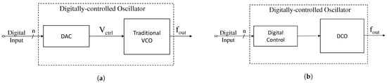
Figure 1.
DCO controlled by (a) DAC, and by a (b) digital controller.
2. General DCO Characteristics
2.1. DAC-Based DCO
Figure 2 shows the block diagram of the DAC-based DCO. The four input bits <A, B, C, D> are given to the 4 × 16 one hot coding-based decoder, which then decodes it to 16 control bits. These control bits are fed to the DAC, which tunes the frequency of the VCO accordingly. Alternatively, the input bits can be given directly to the DAC, which increases the resolution of the DCO. The designed DAC controls the delay time in the delay cell by varying the current through the delay cells. This change in current at the charging and discharging nodes produces the variation in oscillation frequency. The current sources occupy a considerably smaller area and consume less power. The output of the oscillator should drive large transistors, hence the output of the oscillator I+, I−, Q+ and Q− are passed on to the corresponding buffers.
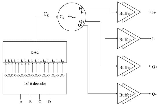
Figure 2.
Block diagram of the DAC-based DCO [7].
The DAC-based DCO is designed differentially with four delay cells, which are controlled with the help of a control signal (Cs) from the DAC, as shown in Figure 3a. A cross-coupled architecture is chosen for the delay cell, as it provides better phase noise and jitter performance. The delay from the cross-coupled architecture is regulated by varying the node currents by the Cs. A differential ring-oscillator structurem, as shown in Figure 3b, is chosen due to its high stability, strong robust against substrate and supply noise, and its capability to generate in-phase and quadrature signal components.
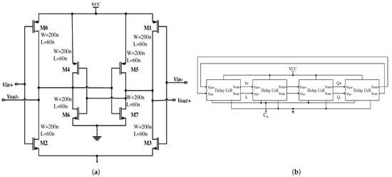
Figure 3.
(a) Schematic of delay cell, (b) Block diagram of the ring oscillator [7].
Cs is derived from the current source, a weighted transistor array, as shown in Figure 4. To obtain linear and fine-tuning of the DCO, the pMOS transistors are arranged in increasing order of their size. The size of the (n + 1)th pMOS transistor is increased by the step of the smallest size of the pMOS transistor. The frequency of oscillation increases as the size of the transistor increases, due to the higher current through the delay cells. Cs is obtained from the nMOS transistor, which is always ON. This keeps the output capacitance of the DAC independent of the weighted pMOS transistors, which helps to change the oscillation frequency linearly. Each pMOS transistor in the DAC can be designed independently, as only one pMOS transistor becomes active at a given time. This grants the freedom to assign custom frequencies to a digital code, by tuning the size of the pMOS transistor. The control bits for the DAC can be directly obtained from the digital loop filter (DLF) or via a decoder. Obtaining the control bits directly from the DLF improves the resolution of the DCO to [7].
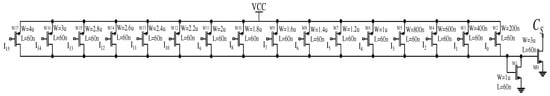
Figure 4.
Schematic of the DAC [7].
2.2. Controller-Based DCO
Figure 5 shows the block diagram for the controller-based DCO. The row and column control signals are obtained from the controller and the frequency is tuned accordingly. The dither control signals are acquired from the delta-sigma modulator and they are used for fine-tuning of the DPLL. The three-stage ring oscillator in the proposed design consists of four rows and six columns of CMOS inverters. The schematic of the delay cell is as shown in Figure 6. Each stage of the oscillator is connected in parallel. The frequency of the DCO is tuned by increasing or decreasing the size of the transistors, which changes the charge/discharge current through the transistors. When the size of transistors M0 and M3 increase, the oscillation frequency and frequency tuning range of the DCO increases. The frequency tuning range decreases when the size of M4 and M5 increases, but the oscillation frequency shifts upwards. As more inverters are turned ON, the oscillation frequency of the DCO increases, at the same time as the current driving capability of the inverters increases. The inverter is controlled by the signals from the row control, column control, and row-override blocks. An inverter is turned ON when both row and column-control signals are logic HIGH or the signal row-override signal is logic HIGH.
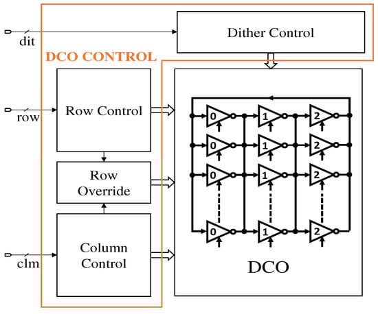
Figure 5.
Block diagram of controller-based DCO.
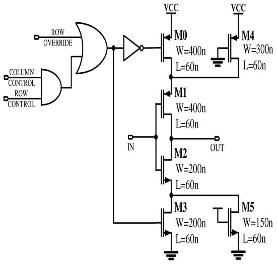
Figure 6.
Schematic of the delay cell.
The rows and columns of the oscillator are adjusted by the digital controller, as illustrated in Figure 7. The controller receives the SIGN signal as input, based on which the counter starts counting up or down. The SIGN signal is obtained from the PFD, which transmits the information whether the reference signal is leading or lagging. The input CLK signal is the delayed version of the reference signal. The ENFINE signal controls the counter and register clock. These blocks only operate when the ENFINE signal is logic LOW. The register clock block generates two clocks, CLKMAX and CLKMIN signals based on the SIGN, CLKREF and ENFINE signals. Based on these clocks, the register block stores the last two maximum and minimum values of the output states of the counter. These values are then passed on to the control check block. This block verifies whether the two maximum and minimum values are close enough. In the proposed design, the threshold is set to 2, whcih is, If the difference between the maximum or the minimum values stored is less than or equal to 2, then the signal ENFINE is set HIGH. Additionally, the control check block loads the average of the last maximum and minimum value to the multiplexer. The ENFINE signal toggles the multiplexer output and disables the clock to the counter and the register clock block, thus enabling the fine-tuning for DPLL. The LSB signals from the multiplexer are transmitted to the column-control block and the MSB signals to the row-control block. These blocks are identical digital blocks, which select the row and column of the DCO according to the multiplexer output.
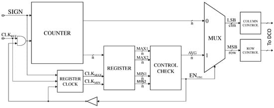
Figure 7.
Block diagram of the controller.
When the counter increases by one, the controller turns ON one more delay cell, which is shown in Figure 6, from the same partially turned ON row. After all inverters in the current row are turned ON, then the first inverter in the next row is turned ON. That is, when the column reaches its maximum, then the column resets to its first column and the row increases by one. Similarly, when the counter decreases by one, the counters acts in the reverse direction. In the proposed design, the oscillator oscillates between 5.252 GHz and 6.344 GHz with 25 steps. The gain of the DCO is 48 /LSB.
3. Layout and Simulation Results
The layouts of the DAC-based DCO and the controller-based DCO with an area of 36.33 μm2 and 550 μm2 in TSMC 65 nm CMOS technology, respectively, are shown in Figure 8. The blank space on the top in the controller-based DCO can be used for implementing the dither control, which makes the layout more compact. All of the simulations are performed with extracted RC parasitics from the layout. Whereas, the DAC-based differential ring oscillator oscillates between and , consuming an average power of . The designed controller-based DCO operates between and , and it consumes an average power of . Both of the oscillators operates from and the power is measured with the oscillators running at their highest frequency along with their control circuit and the buffers.
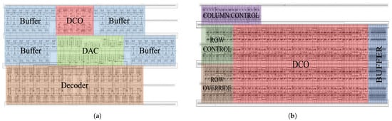
Figure 8.
Layout of the (a) DAC-based DCO, (b) Controller-based DCO.
Figure 9 sows the phase noise characteristics of the free running oscillator in both types. The phase noise performance can be improved by using the DCO in a closed-loop system with proper loop filter adjustment. The phase noise of the DAC-based DCO and controller-based DCO at 2.2 GHz and 6.4 GHz is −78.9 dBc/Hz and −81.3 dBc/Hz at 1 MHz offset, respectively. The jitter performance of the DCOs is measured from the eye diagram at their highest operating frequency. The peak-to-peak jitter obtained for the DAC-based DCO is 8.7 ps and for the controller-based DCO is 6.8 ps at 2.2 GHz and 6.4 GHz, respectively, as shown in Figure 10. The spectrum of the DAC-based DAC at 2.2 GHz and controller-based DCO at 6.34 GHz is shown in Figure 11. The spectrum is a measure of distortions to the signal by other noise sources. The Spurious Free Dynamic Range (SFDR) of the DAC-based and controller-based DCO at 125 MHz is 77.2 dBc and 56.8 dBc, respectively. DAC-based and controller-based DCOs both show a linear behaviour with increase in input control bits. Monte Carlo simulations are performed for both the DAC-based and controller-based DCOs, and the deviation of 7.4% and 8.5% was observed in the output frequency.
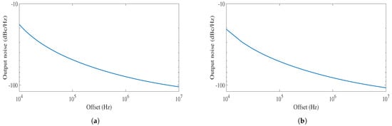
Figure 9.
Phase noise performance of the (a) DAC-based DCO, (b) Controller-based DCO.
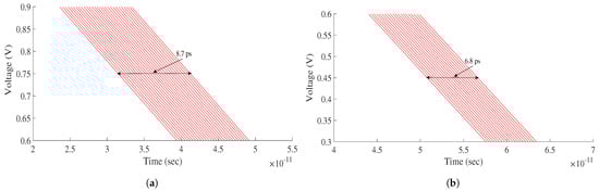
Figure 10.
Jitter of the (a) DAC-based DCO at 2.2 GHz, (b) Controller-based DCO at 6.4 GHz.
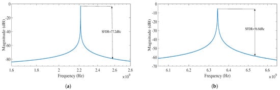
Figure 11.
Spectrum of the (a) DAC-based DCO at 2.2 GHz, (b) Controller-based DCO at 6.4 GHz.
Table 1 shows a comparison with state-of-the-art ADPLL. The DAC-based DCO and controller-based DCO outperform the state-of-the-art designs in terms of area and power consumption. The implemented DAC-based DCO gives an advantage in terms of the resolution and step size of the frequency shifting of the ring oscillator due to the analogue behaviour of the design. On the other hand, the proposed design may suffer from the process variation since the size relation between current charging transistors in the DAC directly affect the analogue output control voltage that changes based on digital input data. The second implementation which is the fully digital controller-based DCO does not require any precise current charging capability. Thus, the process variation can have a less effect on the working principle of the proposed controller. Additionally, since this locking step primarily controlled by the SIGN signal generated by a conventional phase detector, the robustness of the controller is further improved against process variation as compared to the conventional time-to-digital converter (TDC) based controller, which makes them sensitive to the any changes in resolution. The Figure-of-Merit for jitter (FOMjitter) of the DAC-based and controller-based DCO outperform [8], and they are almost the same with [9]. The [10] is based on the schematic simulation, hence the FOMjitter is better than the proposed designs. The DCO in [11] is designed using 28 technology and it uses LC-tank based architecture. Hence, the phase noise performance of [11] is better than the DAC-based and controller-based DCO. However, its active area is much larger than the proposed DAC-based and controller-based DCO in spite of the DCO that was implemented in 28 . The DAC-based DCO and controller-based DCO outperform [8,9] in terms of peak-to-peak jitter performance. The proposed design uses a simple architecture and it occupies a less active area. Hence, for SoC applications where multiple PLLs are required, the introduced locking techniques, especially the fully digital controller-based DCO, occupy smaller active with comparable performance compared to state-of-the-art designs.

Table 1.
Performance Summary and comparison with state-of-the-art.
4. Conclusions
A DAC-based DCO and controller-based DCO are designed using TSMC 65 CMOS technology. The DAC-based DCO is designed with four digitally-controlled differential stages leading to a tuning range from to . The controller-based DCO is designed with three digitally-controlled stages that can be tuned from to . The DAC-based DCO provides better resolution than the controller-based DCO, as the DAC-based architecture is analogue in nature. However, the resolution of the controller-based architecture can be increased by adding dithering stages controlled by a delta-sigma modulator. For both architectures, the layout is constructed, verified with DRS and LVS, and the parasitic components of the layout version are extracted. The designs are checked for their phase noise performance, peak-to-peak distortions, and for their jitter performance. The designs are small in size and are linear in nature.
Author Contributions
Writing—original draft preparation, S.S.; writing—review and editing, E.B., R.N. All authors have read and agreed to the published version of the manuscript.
Funding
This work was supported by the German Research Foundation (DFG) under contract no. NE 1877/1-2.
Institutional Review Board Statement
Not applicable.
Informed Consent Statement
Not applicable.
Data Availability Statement
Not applicable.
Conflicts of Interest
The authors declare no conflict of interest.
References
- Egan, W.F. Phase-Lock Basics; Wiley: Hoboken, NJ, USA, 2007. [Google Scholar]
- Razavi, B. Phase-Locking in High-Performance Systems: From Devices to Architectures; Wiley: Hoboken, NJ, USA, 2003. [Google Scholar]
- Stephens, D.R. Phase-Locked Loops for Wireless Communications Digital, Analog and Optical Implementations; Kluwer Academic Publishers: New York, NY, USA, 2002. [Google Scholar]
- Razavi, B. Design of Analog CMOS Integrated Circuit Design; Mc-Graw Hill: New York, NY, USA, 2001. [Google Scholar]
- Godave, A.; Choudhari, P.; Jadhav, A. Comparison and Simulation of Analog and Digital Phase Locked Loop. In Proceedings of the 2018 9th International Conference on Computing, Communication and Networking Technologies (ICCCNT), Bengaluru, India, 10–12 July 2018. [Google Scholar]
- Wolaver, D.H. Phase-Locked Loop Circuit Design; Prentice Hall: Hoboken, NJ, USA, 1991. [Google Scholar]
- Selvaraj, S.; Bayram, E.; Negra, R. Low phase noise, high resolution digitally-controlled ring oscillator operating at 2.2 GHz. In In Proceedings of the 2020 9th International Conference on Modern Circuits and Systems Technologies (MOCAST), Bremen, Germany, 7–9 September 2020; pp. 1–4. [Google Scholar] [CrossRef]
- Deng, X.; Mo, Y.; Lin, X.; Zhu, M. A 0.68-to-1.44 GHz low-jitter all-digital phase-locked loop with a novel PFD and a high resolution DCO in 0.18 μm CMOS. In Proceedings of the 2016 IEEE International Conference on Electron Devices and Solid-State Circuits (EDSSC), Hong Kong, China, 3–5 August 2016. [Google Scholar]
- Luo, Z.; Wang, G.; Yousef, K.; Lau, B.; Lian, Y.; Heng, C. A 0.0129 mm2 DPLL with 1.6 2.0 ps RMS Period Jitter and 0.25-to-2.7 GHz Tunable DCO Frequency Range in 55-nm CMOS. In Proceedings of the IEEE Transactions on Circuits and Systems II: Express Briefs, Beijing, China, 16–18 October 2018. [Google Scholar]
- Gorgi, J.; Ghaznavi-Ghoushchi, M.B. A 2.7 to 4.6 GHz Multi-Phase High Resolution and Wide Tuning Range Digitally-Controlled Oscillator in CMOS 65 nm. In Proceedings of the 24th Iranian Conferenece on Electrical Engineering (ICEE), Shiraz, Iran, 10–12 May 2016. [Google Scholar]
- Levinger, R.; Levi, R.; Shumaker, E.; Levin, S.; Horovitz, G. A 3.9–4.7 GHz 0.35 mW DCO with −187.4 dBc FoM in 28 nm CMOS. In Proceedings of the 2018 13th European Microwave Integrated Circuits Conference (EuMIC), Madrid, Spain, 23–25 September 2018. [Google Scholar]
Publisher’s Note: MDPI stays neutral with regard to jurisdictional claims in published maps and institutional affiliations. |
© 2021 by the authors. Licensee MDPI, Basel, Switzerland. This article is an open access article distributed under the terms and conditions of the Creative Commons Attribution (CC BY) license (https://creativecommons.org/licenses/by/4.0/).