Abstract
Simultaneous wireless power and data transfer (SWPDT) technology is usually needed in wireless power transfer (WPT) systems. In this paper, to achieve the efficient and stable SWPDT, the signal to noise rate (SNR) is first optimized through the analysis of data transmission gain and the interference of power transfer on data transfer. In order to reduce the interference of power channel to data transfer channel, the compensation topology of double-sided LCC and the band-stop networks are used. To solve the problem of SNR limitation, the coupling relationships between each circuit are taken into consideration and a matching method of resonance parameters to improve the SNR is presented. Based on the relationship between SNR and the parameters of data transfer channel, an optimization design method focused on parameters of data transfer channel for improving the SNR is presented. Finally, the feasibility and the correctness of the parameter design method proposed in this paper is verified by simulation and experiment.
1. Introduction
Owing to the stability, flexibility, and high efficiency, wireless power transfer (WPT) technology is becoming more and more popular, and it has been applied in many fields, such as electric vehicles, mobile phones, wireless sensors, medical equipment, robotics [1,2,3,4], etc. As far as the application of WPT technology is concerned, data transmission between the transmitter side and receiver side is usually needed to implement the feedback control of power flow, the state monitoring of the system, the detection of load and foreign objects, etc. Therefore, the research on the simultaneous wireless power and data transfer (SWPDT) has attracted more and more attention.
Generally, in terms of data transfer, there are four major methods of data transfer to achieve SWPDT. The first data transfer method is to use the communication module, such as Bluetooth module, ZigBee, Wi-Fi, etc. However, there are some problems to use these modules in a WPT system [5,6], such as the delay time for the communication establishment and the complex pairing between the transmitter side and receiver side. Therefore, the stability of the information interaction process cannot be guaranteed.
The second data transfer method is by adding a pair of data transfer coils [7,8,9,10,11]. In references [7,8], the parameters of data transfer coil were optimized considering the cross-coupling between the power link and data link. In the reference [9], the omnidirectional wireless power transfer system with 3-D transmitter coil utilized for data and power transfer at different position was proposed. In references [10,11], the decoupling coils of data and power transfer coil were proposed to eliminate the interference from power flow on data transmission. The advantages of this method is that it could not only avoid frequency interference with other communication devices, but also realize full duplex communication effectively. However, this method also has some disadvantages, such as the cross-coupling between the data transfer coils and power transfer coils, and reducing the flexibility of WPT systems by adding the signal coils.
The third data transfer method is by using power wave modulation, i.e., taking power waveform as carrier, and data is modulated by changing the amplitude, the frequency, or the phase of power carrier. In the reference [12], data are modulated by changing the phase of the power amplifier, and the achieved data transfer rate is 125 kb/s, while the output voltage is 5 V. In references [13,14], the data modulation is realized with the 15 kb/s data rate by adjusting the impedance of the load end to change the current or voltage amplitude in primary side. In references [15,16], on the basis of amplitude modulation, the modulation depth of amplitude modulation is optimized to reduce the impact of amplitude fluctuation on power, and the bandwidth of the data is increased through compensation circuit. In reference [17], phase modulation (QAM) is carried out to transfer data based on the high-order harmonic of power flow to improve the data transmission rate. The power modulation method is cost effective to some content, because it can avoid the using of data transfer coils and communication modules. However, this method will inevitably lead to output power fluctuation. Moreover, it is not conducive to the bidirectional data transmission.
The fourth data transfer method is to use the inherent power transfer coils as shown in the Figure 1. The data modulation frequency is usually much higher than the power transfer frequency. In references [18,19,20], the power transmission is realized by magnetic coupling while the data transmission is realized by electric coupling based on the coupling mechanism. In reference [21], the data transfer is achieved with the partial coil while the data transmission gain is −10 dB. In references [22,23,24,25], the coupled transformers are used to inject or extract the modulated data waveforms while the SNRs demonstrated in [22,23,24,25] are below 10 dB. Since no additional coil is required, this method is easy to implement and the system volume using this method is relatively small. Moreover, it can also achieve bidirectional data transfer without power transfer distortion. However, the crosstalk between the power transfer channel and the data transfer channel is large and they are susceptible to parameter perturbations. In addition, currently, the analysis of data transmission gain and the optimization of data transfer channel parameters are still lacking.
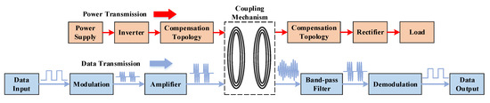
Figure 1.
Data and power transmission achieved by power transfer coils.
To fill the technical gap, in this paper, a novel channel parameter optimization method is presented, which can improve the data transmission gain and ensure that the data demodulation process is not affected by power transfer. Based on parallel injection and extraction, the interference of data to power channel could be effectively blocked. In the power channel, the constant-current characteristic of LCC topology could be used to achieve efficient and stable power transmission, and the filter characteristics of band-stop network whose center frequency is the same with data carrier can reduce the interference of energy to the data channel. The relationship between SNR and channel parameters is deduced by analyzing the impedance of each circuits of the data channel. Based on this, an optimum design method of channel parameters to improve the SNR is presented. A SWPDT system with 88 W output power and 40 kbps data rate is implemented. The correctness and feasibility of the optimized design method is verified by the experimental results.
2. Proposed SWPDT System
The proposed SWPDT system is shown in the Figure 2, which is composed of power transfer channel and data transfer channel. The power transfer channel is composed of a DC power supply, a full-bridge inverter, an LCC compensation network, a coupling mechanism, a rectifier, and a load. The data transfer channel is composed of a data source, coupled transformers, compensation capacitors, adjustment resistances, and an output network.
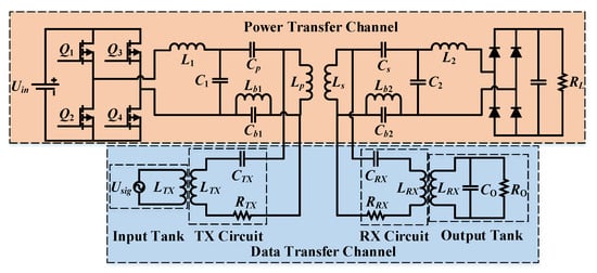
Figure 2.
Simultaneous wireless power and data transfer (SWPDT) system with parallel connection
The working frequency of the inverter is ωp. The LCC compensation network consisting of L1, C1 and Cp (L2, C2 and Cs) is chosen to be applied in this paper for its characteristic to keep the coil current constant and good performance to reduce the interference of power channel on data transfer channel. At the end of the LCC compensation network, a band-stop network consisting of a parallel LC network consisting of Lb1 and Cb1 (Lb2 and Cb2) is connected with the coupling mechanism to block the power flow from covering up the data voltage. The center frequency of band-stop network is the data carrier’s frequency ωd.
The data carrier frequency ωd is much higher than the power working frequency ωp. Generally, the carrier frequency is at least ten times than the power working frequency, i.e., ωd > 10ωp. So the power transfer channel would be in high-impedance state at the data carrier frequency due to the band-stop network.
The mutual inductance of the coupling mechanism is M. The load is connected with the rectifier after the LCC compensation and the equivalent load is RE which satisfies:
The data transmission is also based on magnetic coupling and the modulation is based on amplitude shift keying (ASK). The whole data channel is divided into four parts: input tank, transmitter circuit (TX circuit), receiver circuit (RX circuit) and output tank. The data source presents the ASK modulated wave. There are two coupled transformers taken as the injection and extraction circuit for data carrier in the data channel. It is worth mentioning that at the data carrier frequency the resistance of the transformer is RM which cannot be negligible. CTX and CRX are the resonant capacitors to pass the data carrier and promote the output amplitude. RTX and RRX are the adjustment resistance to alter the output amplitude of data. The data channel is parallel connected with the coupling mechanism. The output circuit is the parallel RLC resonant circuit to extract the modulated wave and filter the interference of the power flow.
To realize the bidirectional data transmission, there are two complementary switches (Qd1, Qd2) changing the circuit state between TX and RX circuit. When Qd1 is on and Qd2 is off, data transfer channel is working at forward data transmission. When Qd1 is off and Qd2 is on, data transfer channel is working at backward data transmission. Therefore, the half-duplex communication could be achieved as shown in the Figure 3.
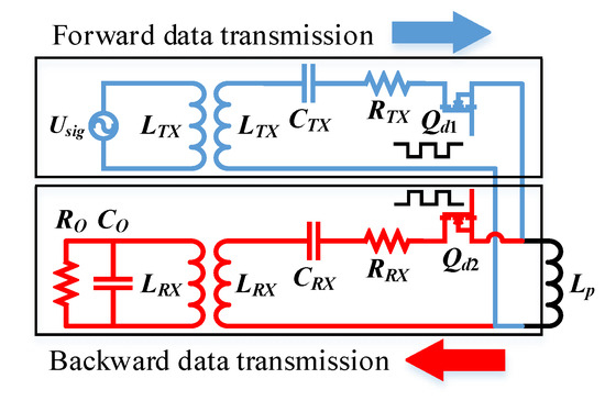
Figure 3.
The half-duplex bidirectional data transmission.
3. Analysis of Power Transfer Channel
In the SWPDT system, the power transfer channel transmits the power flow and the data channel transmits the data at the same time. At the power frequency, the data channel should be in the high-impedance state so as to avoid the impact of data on resonance. At the data carrier frequency, the power channel is in the high-impedance state for existence of the band-stop network, so the influence between power and data is negligible theoretically. However, the resonance is altered due to the existence of band-stop network in the power channel. The amplitude of power interference on data channel would still exist even with the band-stop network in power channel, and the data output voltage would be very low if the parameters are not designed properly. Therefore, the impedance of each channel should be analyzed elaborately for the efficient power transmission and the sustainable data transmission.
The power supply is converted as AC current by full-bridge inverter, and the source is equivalent to Uin. The data source should be treated as short-circuit source, and when the equivalent circuit of the power channel is shown in Figure 4.
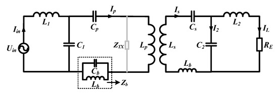
Figure 4.
Equivalent circuit of power channel.
On the primary side of the power channel, the TX circuit is parallel connected with the coil and the impedance of the TX circuit is ZTX. The value of ZTX could be calculated:
It should be noted that the power frequency is much smaller than the data carrier frequency. The impedance of the TX circuit is very high at the power frequency, so the influence of TX circuit could be neglected since it is in high-impedance state parallel connected with the compensation topology. And the RX circuit is also in high-impedance state at power transfer frequency. Assuming that the band-stop networks are identical, the impedance of the band-stop network is Zb and the value of the network is approximately equal to its inductance at the power frequency.
So, the resonant frequency is changed due to the addition of band-stop network. In order to keep resonant frequency unchanged, the inductance of Zb must be taken into consideration during the calculation. The primary side of power channel could be modelled by Kirchhoff’s current law (KCL) and Kirchhoff’s voltage law (KVL):
where Zr is the reflection impedance from secondary side. To realize the constant current of the coil Ip and eliminate the imaginary part of the circuit, the resonance parameters could be derived:
Substituting (6) into (5) the expression of Ip could be derived
It is obvious that the current of the coil Ip is constant only if the L1 is unchanged. In the practical application, the inductance of L1 could be guaranteed to be steady while the power is transmitted.
The secondary side of the power channel is analyzed similarly. The equation of the secondary side could be obtained:
According to the resonant principle of LCC topology, those resonance parameters of the secondary side could be derived as the primary side:
All the parameters of power channel are obtained by the resonant principle of LCC topology, so the current and the output power of the load are also obtained based on (5)–(9):
In (10), the current of the load IL is constant when the mutual inductance is unchanged and steady at a wide load range.
Therefore, the current of the primary coil could be constant, and the current of the load is only related to the mutual inductance M. The inductances L1 and L2 should be elaborately designed for the appropriate requirements for coil current and load voltage.
Through the above analysis, the influence of the data branch circuits (TX circuit and RX circuit) on the power channel can be ignored because of their high impedances. After adding the band-stop network Zb, the inductance value of it should be considered in the resonance parameters of LCC topology, so the influence of extra inductance value on the resonance parameters should be eliminated by compensation. Therefore, the power channel could be kept in the resonant state and high efficiency.
4. Analysis of Data Transfer Channel
In this paper, the data transmission could be in only one direction at a certain moment. Therefore, the forward direction is taken as an example and the analysis is presented based on the equivalent circuit of the forward direction shown in the Figure 5.
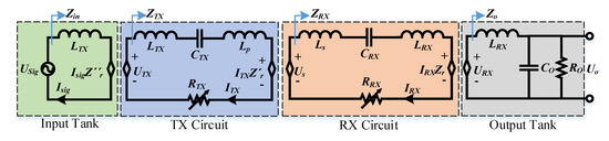
Figure 5.
Equivalent circuit of the data channel in forward direction.
There are four parts in the data channel: input tank, TX circuit, RX circuit and output tank. The data source is connected with the coupled transformer directly, which forms the input tank. The inductances of primary side and secondary side are identical (LTX) and the internal resistance of the transformer is noted as RM which is not negligible at the data carrier frequency. The TX circuit and RX circuit work as the band-pass filter to improve the amplitude of the data carrier. The influence on the power channel parallel connected with the coil is reduced significantly by the band-stop network. The output tank is a parallel RLC network to improve the amplitude of the data carrier, besides which the interference could be reduced by the RLC network further.
4.1. Output Tank and RX Circuit
The impedance of the output tank could be obtained based on the parallel RLC tank, and the resonant parameters are confirmed by the carrier frequency to improve the amplitude and filter the other interference.
So, the impedance of the output tank could be obtained by the resonant parameters.
Therefore, the relationship between the output voltage and induced voltage on the secondary side of LRX could be derived.
Under the affection of the coupled transformer, the reflection impedance from the secondary side is Zr.
The real part and imaginary part of the reflection impedance Zr are presented as following:
where the kRX is the coupling coefficient of the coupled transformer between RX circuit and output tank.
The reflection impedance should be taken into consideration during the calculation on the impedance of the RX circuit. So, the impedance of the RX circuit ZRX could be obtained.
According to (16), the real part of ZRX is the addition of RRX, RM and the real part of reflection impedance. The imaginary part of ZRX is the addition of CRX, LS, LRX and the imaginary part of reflection impedance. The current of the RX circuit could be kept as resonant if the imaginary part were zero constantly. So, the relationships of parameters are acquired based on the resonance and impedance of the RX circuit.
When the resonant parameters of RX circuit meet (17), Im(ZRX) = 0, that is, the imaginary part of RX circuit impedance is zero, the current would reach the maximum and the amplitude of output voltage would also reach the maximum. Furthermore, the relationship between the data output voltage and induced voltage on LS can be deduced
4.2. RX Circuit and TX Circuit
The coupling relationship between RX circuit and TX circuit is similar to that of power channel, and the reflection impedance from RX circuit to TX circuit is noted as Zr’. Through the above analysis, the imaginary of ZRX is zero and the reflection impedance is deduced.
From (19), there is no imaginary part of the reflection impedance, so the resonance on the TX circuit would not be affected by the RX circuit only if the parameters on RX circuit are met with the (17). The impedance of the TX circuit is noted as ZTX
Therefore, the relationship between the induced voltage on LTX and the output voltage could be obtained.
4.3. TX Circuit and Input Tank
In the input tank, there are the inductance LTX and internal resistance RM of the coupled transformer, but the reflection impedance must be taken into consideration. Obviously, the impedance of input tank is inductive if there is no influence on the reflection impedance. To improve the current of input tank, the imaginary part should be eliminated by the reflection impedance noted as Zr″ from the TX circuit. The reflection impedance could be derived by (20).
The impedance of the input tank could be obtained easily.
According to (22) and (23), the imaginary part of the input tank would be eliminated only if the impedance of the TX circuit is inductive and the value is matched with the inductance LTX. The impedance of the TX circuit could be expressed as
where the LX and RX are the imaginary part and real part of impedance respectively.
Based on the analysis of TX circuit and input tank, the relationship between their values could be derived.
When the imaginary part of ZTX is met with (25), the imaginary part of input tank would be eliminated. So, the resonance parameters of the TX circuit could be acquired as following:
Furthermore, the conclusion that the resonance parameters on TX circuit (LTX, Lp, CTX) are only related with data carrier frequency and transformer parameters instead of the mutual inductance of the coils and parameters on RX circuit can be drawn. The impedance of the input tank could be obtained since the imaginary part is eliminated.
The current of input tank would reach the maximum when the imaginary part of it was eliminated. Moreover, induced voltage UTX, the induced voltage URX and the output voltage UO would be promoted since the impedances of each circuit were matched to eliminate the imaginary part.
The gain of the data transmission could be deduced based on the impedance of each circuit when the parameters are met with the (11), (17), and (26). The gain noted as Gd is derived as followed:
Obviously, the gain is related with the data carrier frequency ωd, the output resistance Ro, the coupling coefficient kRX and kTX, the adjustment resistances in RX circuit and TX circuit RRX, RTX, and the mutual inductance of the coils M. In addition to the resonance parameters that must be matched based on the (11), (17) and (26), the other parameters of the data channel also need to be optimized.
5. Analysis on Signal to Noise Rate of SWPDT System
The output tank in data transfer channel is also influenced by the power flow even with the band-stop networks in practical, so the noise should be taken into consideration during the calculation of the SNR. And it is obvious that the communication would be failure if the interference covered the data output voltage.
The demodulation circuit is shown in the Figure 6, there are four parts of the demodulation circuit: second-order high-pass filter, amplifier, detection circuit and comparison circuit. Although the impact of power flow would be reduced through second-order high-pass filter, the inductive voltage of power flow still exist in the data transfer channel. So, the higher SNR is expected in the SWPDT system for better performance of communication.
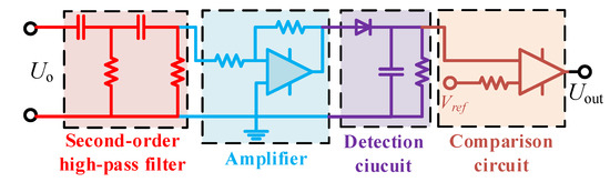
Figure 6.
Demodulation circuit of the proposed SWPDT system.
5.1. Analysis of SNR
The output voltage could be obtained based on the gain of data transmission, and the output voltage is related with the input voltage and the gain.
In generally, the input voltage is constant during the transmission, so the promotion of output voltage should be achieved by increasing the gain of data transmission.
However, the interference of power flow is also induced in the output tank. The power interference gain is Gpd and the induced voltage is Upd. The equivalent circuit of data transfer channel with power flow is shown in the Figure 7.
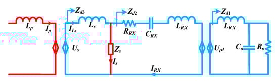
Figure 7.
Equivalent circuit of data transfer channel with power flow.
In Figure 7, the current of the transmitter coil is constant according to the (7), so the induced voltage of receiver coil is stable as the mutual inductance M is kept constant. However, the impedance of data transfer channel would be very high at the power transfer frequency ωp leading to the small current of RX circuit IRX. The impedance of power branch circuit Zs is
The impedance of Zd2 and Zd3 are
where Zd1 is the impedance of the output tank at the power transfer frequency, which is different from its value at the carrier frequency. The impedance of the output tank at the power transfer frequency is presented as follow.
So, the gains of each parts are deduced by the (30)–(32) and (7),
The total gain of power interference could be obtained according to the (33).
The induced voltage of power interference is deduced as follow.
The SNR is deduced by the (29), (35), and the gain of the data transmission is much more than the gain of the power interference.
To increase the SNR of SWPDT system, the increment of data transmission and decrement of power interference are considered by optimization of the data transfer channel.
5.2. Parameters of Data Transfer Channel
Based on the above analysis of the SNR, its enhancement could be achieved by optimizing the data channel parameters which include ωd, Ro, kRX, kTX, RRX, RTX, and M. Each parameter would be discussed separately in this part.
5.2.1. Output Resistance and Mutual Inductance of the Coils
Although the reflection impedance from the RX circuit contained the output resistance, its affection could only be much weakened if the output resistance is far larger than the value of ω2M2 in the (19). The condition of the output resistance is required since it should be large enough to reduce the affection on Zr′.
Therefore, the output resistance should be as large as possible according to the (37) since its influence on the RX circuit is reduced. For a better description of the relationship between Ro and SNR, the curve of Ro and SNR was depicted by simulation software.
As shown in Figure 8a, the SNR is increasing when the output resistance is rising at different mutual inductance M. The growth of SNR tends to be stable when the output resistance Ro reached a certain value. So, the output resistance should be selected as larger as possible in the data channel.
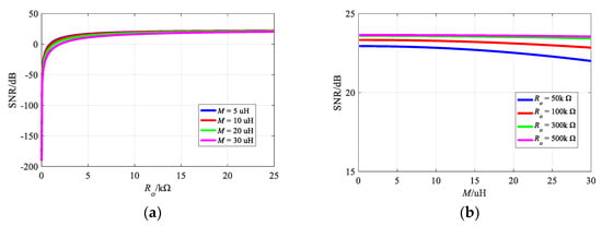
Figure 8.
(a) The signal to noise rate (SNR) versus Ro; (b) SNR versus M.
The SNR shown in the Figure 8b varied little value at a mutual inductance range, so the conclusion that the mutual inductance of two coils has limited affection on SNR could be drawn. The reason why the SNR is not affected by mutual inductance M is that the data transmission and power interference are increasing at the same proportion when the M increases, so the SNR is kept as a stable value at a certain mutual inductance range. It should be noted that the mutual inductance should not be selected as an excessively high value due to the frequency splitting phenomenon reducing the power [26].
5.2.2. Coupling Coefficient kRX and kTX
According to (28) and (36), the curves of SNR are shown in Figure 9a,b. The SNR is increasing as the coupling coefficient kTX increases shown in the (a), while there is an optimal point in the (b) indicating that the coupling coefficient kRX should be selected carefully.
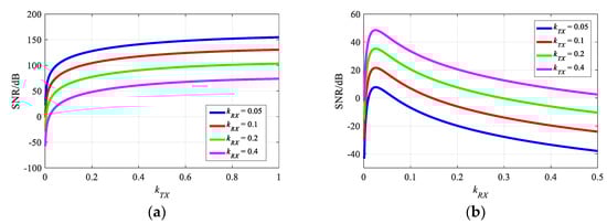
Figure 9.
SNR versus (a) kTX; (b) kRX.
So, the loosely coupled transformer in RX circuit is suitable to select the optimal point since the SNR could be a high level, while the tightly coupled transformer in TX circuit should be selected because of its high value of SNR. For better comprehension of optimal point of coupling coefficient kRX, the optimal point could be deduced by (28) and (36). The optimal point is related with the output resistance and the relationship between them could be depicted in Figure 10. In Figure 10, the curves with same kTX conditions indicate that the optimal points to reach the maximum value of SNR are not identical if the output resistances are different. Generally, the output resistance is much more than the adjustment resistance in RX circuit, so the optimal point is manly decided by the output resistance. The calculation of the optimal point is derived according to (28) and (36) by simulation software
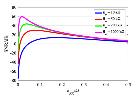
Figure 10.
SNR versus kRX with different Ro.
Above the analysis on the two coupling coefficients, the selection of kTX and kRX is totally different. The transformer in TX circuit with higher coupling coefficient should be selected, while the transformer in RX circuit with optimal point to maximum SNR value should be selected. The optimization of the parameters will be discussed later.
5.2.3. Resistance RTX and RRX
The adjustment resistances to shift the data rate in the data channel are the key factors to affect the amplitude of the data output voltage. The relationship between SNR and RTX/RRX is depicted by the simulation results in Figure 11.
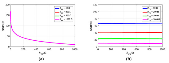
Figure 11.
SNR versus (a) RTX; (b) RRX.
The ranges of SNR is larger when RTX is increasing than that of RRX: the attenuation of SNR is more than 60 dB at the range of 1-1 k ohm of RTX, while the attenuation at the same range of RRX is within 4 dB. So, the effect of RRX on the data transmission could be ignored and stability of the SWPDT system could be promoted achieved by increasing the RRX without attenuation.
The small resistance of the RTX should be selected for a higher amplitude of output voltage. However, it should be pointed out that when the resistance value is too small, a new oscillation will appear in the waveform, which would destroy the integrity of the waveform and cause the data demodulation failure. Therefore, the resistance selection should be taken into consideration carefully for a higher amplitude and complete waveform.
5.3. Design of Data Channel Parameters
The flow chart of the design process is shown in Figure 12, and all the data channel parameters are confirmed based on the above analysis.
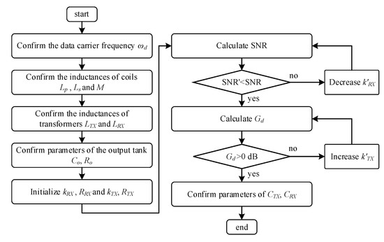
Figure 12.
Flow chart of the design for data channel parameters.
The coils and data carrier frequency are confirmed firstly so the parameters of ωd, Lp, Ls and M are obtained. The transformers are confirmed so that the inductances of primary and secondary are acknowledged. The parameters of output tank could be calculated by the (11) and (29) according to the carrier frequency. After the parameters of output tank are confirmed, the optimal coupling coefficient kRX is calculated by the simulation software in the flow chart and the parameters of RX circuit could be obtained based on the (17). The coupling coefficient kTX could be selected as high as possible to obtain a higher data transmission gain Gd, and the parameters of TX circuit are confirmed by the (26). The adjustment resistance RTX and RRX could be shifted for a faster data rate according to the practical communication requirement.
6. Experimental Verification
After the above analysis, the experimental setup is built to verify the validity of the proposed design shown in the Figure 13. The size of coils fabricated by litz wire is 20 cm × 20 cm, and the gap between them is set to 7 cm. The coupled transformers are also fabricated by litz wire and its size is less than 10 cm × 10 cm. Its height is alterable for the measurement of the coupled coefficient.
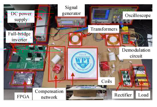
Figure 13.
Experimental setup.
The parameters of the power channel are listed in the Table 1. The working frequency is set to be 85 kHz and the center frequency of the band-stop network is set to 3 MHz which is the data carrier frequency.

Table 1.
Parameters of Power Transfer Channel.
The parameters of the data channel are listed in Table 2. The performance of the data channel is focused on the data transmission gain and power interference. The gains changing with different coupling coefficients are depicted in the Figure 14. As shown in the Figure 14, the trend of curves is consistent with the theoretical analysis in last section. In Figure 14a, the gain is promoting since the coupled coefficient kTX is increasing. It should be noted that the deviation between theoretical and experimental results is caused by the drift of the resonant parameters on the primary side which is more sensitive than secondary side. There is an optimal value to approach the maximum data transmission gain verified by the experimental result in Figure 14b.
Table 2.
Parameters of Data Transfer Channel.
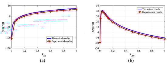
Figure 14.
Experimental results and theoretical results (a) kTX, (b) kRX.
The specific waveforms at the maximum transmission gain condition are shown in the Figure 15 and Figure 16. In the Figure 15, the output voltage of full-bridge inverter is presented as yellow line and the peak-peak value is about 80 V. The output voltage of the load is presented as the purple line and its value is 21 V, so the output power is about 88 W. The current of the coil is presented as green line in the (a), and its value is about 5.57 A which is constant with the theoretical results. As shown in the figures, the frequency of the power flow is shifted to approximately 83 kHz and the deviation is cause by the offset of parameters. The data output voltage is presented as blue line, and it is obvious that the interference of the power transmission is about 1.2 V in the (b). In the (c), the systems are shown with both power transfer and data transfer. The amplitude of data output voltage is about 8 V, which covered the interference of power and the data transmission is not influenced by power flow. Compared with the (b) and (c), the performance of power transmission is not affected by data transmission and the output power is kept as about 88 W.
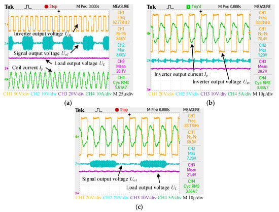
Figure 15.
Waveforms of the power channel and data channel at optimal parameters (a) inverter output voltage, coil current, load output voltage and data output voltage; (b) SWPDT system without data transfer (c) SWPDT system with data transfer.
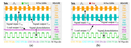
Figure 16.
Waveforms of the data transmission at optimal parameters (a) without power transmission; (b) with power transmission.
The waveforms of data transmission are shown in Figure 15, including the data input, data output and the demodulation output. In the (a), there is only data transmission in the whole system, and the amplitude of the data input presented as yellow line is 3.6 V. The amplitude of data output presented as blue line is about 8.8 V, so the data transmission gain is about 17 dB and the SNR of data carrier is about 40 dB. In the (b), data transmission is with the power transmission at the same time. The load output voltage presented as purple line is 21.7 V which means the power is transmitted to load and the data output is not covered by the interference of power. Obviously, the data transmission is still affected by power flow, especially the data input whose fluctuation is more obvious than that of data output. Due to the high data transmission gain, the fluctuation on data output would not affect demodulation process. The demodulation data is presented as green line and its frequency is 20 kHz, namely 40 kbps data rate.
The delay time of data transmission is shown in the Figure 17. The delay time (td1) between data input and output is less than 1μs. And the whole delay time (td1 + td2) is 3 μs. The delay time fulfills the most communication condition in most WPT applications. So, the data rate is selected as 40 kb/s since it is satisfied with most applications of WPT systems and it is not affected by the delay time.
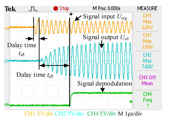
Figure 17.
Delay time of data transmission.
The comparison between the proposed data channel design method and other researches is presented in the Figure 18. Through the comparison, we can conclude that the SNR of proposed system is promoted by optimization, especially under the higher carrier frequency condition. Apparently, the higher carrier frequency could be selected to improve SNR according to the works [23,24,25]. However, the higher SNR could be acquired in this paper without increasing the data carrier frequency.
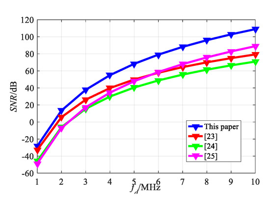
Figure 18.
Comparison between different works.
7. Conclusions
The analysis of the SWPDT system based on the double-sided LCC compensation and parallel injection/extraction of data transmission is presented and the optimization of parameters to improve the SNR is proposed in this paper. The interference of the power channel could be effectively blocked by the double-sided LCC compensation in addition to the band-stop network. The impedance of each part in the data channel is analyzed to fulfill the resonance condition and the data transmission gain is deduced based on the parameters of the data channel. To improve the SNR further, those parameters are optimized based on the analysis of SNR, especially the coupling coefficient of the transformers. An experimental setup is built, and the power channel is transferred with stable state while the amplitude of the data output voltage is improved compared with former researches. The proposed SWPDT system can be used in wireless charging systems for implantable devices, wireless sensors, robots, and mobile phones.
Author Contributions
In this work, Y.S. designed the topology and inspired the communication mode. P.W. proposed the optimization method and analyzed both power transfer channel and data transfer channel. P.W. has also conducted measurements in the prototype model, writing, and formatting of this manuscript. X.L. and Z.Y. have supported the experimental and revised the manuscript. All authors have read and agreed to the published version of the manuscript.
Funding
This research was funded by National Natural Science Foundation of China, grant number 62073047.
Acknowledgments
Authors of this paper gratefully acknowledge the support of China National Center for International Research on Wireless Power Transfer Technology.
Conflicts of Interest
The authors declare no conflict of interest.
References
- Zhao, Z.; Liu, F.; Chen, K. New progress of wireless charging technology for electric vehicles. Trans. China Electrotech. Soc. 2016, 31, 30–40. [Google Scholar]
- Hui, S.Y. Planar Wireless Charging Technology for Portable Electronic Products and Qi. Proc. IEEE 2013, 101, 1290–1301. [Google Scholar] [CrossRef]
- Cairo, J.I.; Bonache, J.; Paredes, F.; Martin, F. Reconfigurable System for Wireless Power Transfer (WPT) and Near Field Communications (NFC). IEEE J. Radio Freq. Identif. 2017, 1, 253–259. [Google Scholar] [CrossRef]
- Ahmadi, M.M.; Ghandi, S. A Class-E Power Amplifier with Wideband FSK Modulation for Inductive Power and Data Transmission to Medical Implants. IEEE Sens. J. 2018, 18, 7242–7252. [Google Scholar] [CrossRef]
- Brusamarello, V.J.; Blauth, Y.B.; De Azambuja, R.; Muller, I.; De Sousa, F.R. Power Transfer With an Inductive Link and Wireless Tuning. IEEE Trans. Instrum. Meas. 2013, 62, 924–931. [Google Scholar] [CrossRef]
- Si, P.; Hu, A.P.; Malpas, S.; Budgett, D. A Frequency Control Method for Regulating Wireless Power to Implantable Devices. IEEE Trans. Biomed. Circuits Syst. 2008, 2, 22–29. [Google Scholar] [CrossRef]
- Simard, G.; Sawan, M.; Massicotte, D. High-Speed OQPSK and Efficient Power Transfer through Inductive Link for Biomedical Implants. IEEE Trans. Biomed. Circuits Syst. 2010, 4, 192–200. [Google Scholar] [CrossRef]
- Wang, G.; Wang, P.; Tang, Y.; Liu, W. Analysis of Dual Band Power and Data Telemetry for Biomedical Implants. IEEE Trans. Biomed. Circuits Syst. 2012, 6, 208–215. [Google Scholar] [CrossRef]
- Narayanamoorthi, R.; Juliet, A.V. IoT-Enabled Home Cage with Three-Dimensional Resonant Wireless Power and Data Transfer Scheme for Freely Moving Animal. IEEE Sens. J. 2018, 18, 8154–8161. [Google Scholar] [CrossRef]
- Lee, W.; Park, S.; Lee, J.-H.; Tentzeris, M.M. Longitudinally Misalignment-Insensitive Dual-Band Wireless Power and Data Transfer Systems for a Position Detection of Fast-Moving Vehicles. IEEE Trans. Antennas Propag. 2019, 67, 5614–5622. [Google Scholar] [CrossRef]
- Zouaoui, S.; Souilem, M.; Dghais, W.; Radwan, A.; Barmada, S.; Tucci, M. Wireless Power Transfer and Data Communication Cognitive Radio through Two-Coil Inductive Channel. In Proceedings of the 2019 IEEE Global Communications Conference (GLOBECOM), Waikoloa, HI, USA, 9–13 December 2019; pp. 1–6. [Google Scholar]
- Peng, K.; Tang, X.; Mai, S.; Wang, Z. A Simultaneous Power and Downlink Data Transfer System with Pulse Phase Modulation. IEEE Trans. Circuits Syst. II Express Briefs 2019, 66, 808–812. [Google Scholar] [CrossRef]
- Mao, S.; Wang, H.; Zhu, C.; Mao, Z.-H.; Sun, M. Simultaneous wireless power transfer and data communication using synchronous pulse-controlled load modulation. Measurement 2017, 109, 316–325. [Google Scholar] [CrossRef] [PubMed]
- Li, X.; Tsui, C.-Y.; Ki, W.-H. A 13.56 MHz Wireless Power Transfer System with Reconfigurable Resonant Regulating Rectifier and Wireless Power Control for Implantable Medical Devices. IEEE J. Solid-State Circuits 2015, 50, 978–989. [Google Scholar] [CrossRef]
- Ye, D.; Wang, Y.; Xiang, Y.; Lyu, L.; Min, H.; Liu, S. A Wireless Power and Data Transfer Receiver Achieving 75.4% Effective Power Conversion Efficiency and Supporting 0.1% Modulation Depth for ASK Demodulation. IEEE J. Solid-State Circuits 2020, 55, 1386–1400. [Google Scholar] [CrossRef]
- Wang, L.; Li, X.; Raju, S.; Yue, C.P. Simultaneous Magnetic Resonance Wireless Power and High-Speed Data Transfer System With Cascaded Equalizer for Variable Channel Compensation. IEEE Trans. Power Electron. 2019, 34, 11594–11604. [Google Scholar] [CrossRef]
- Besnoff, J.; Abbasi, M.; Ricketts, D.S. High Data-Rate Communication in Near-Field RFID and Wireless Power Using Higher Order Modulation. IEEE Trans. Microw. Theory Tech. 2016, 64, 1–13. [Google Scholar] [CrossRef]
- Yu, T.-C.; Huang, W.-H.; Yang, C.-L. Design of Dual Frequency Mixed Coupling Coils of Wireless Power and Data Transfer to Enhance Lateral and Angular Misalignment Tolerance. IEEE J. Electromagn. RF Microwaves Med. Biol. 2019, 3, 216–223. [Google Scholar] [CrossRef]
- Freitas, S.V.D.C.D.; Domingos, F.C.; Mirzavand, R.; Maunder, A.; Naseri, P.; Mousavi, P. A Novel Method for Data and Power Transmission through Metallic Structures. IEEE Trans. Ind. Electron. 2016, 64, 4027–4036. [Google Scholar] [CrossRef]
- Li, X.; Tang, C.; Dai, X.; Deng, P.; Su, Y. An Inductive and Capacitive Combined Parallel Transmission of Power and Data for Wireless Power Transfer Systems. IEEE Trans. Power Electron. 2018, 33, 4980–4991. [Google Scholar] [CrossRef]
- Machnoor, M.; Paknahad, J.; Stang, J.; Lazzi, G. Wireless Telemetry System with Independent Power and Data Frequency Resonance. IEEE Antennas Wirel. Propag. Lett. 2020, 19, 690–694. [Google Scholar] [CrossRef]
- Wu, J.; Zhao, C.; Lin, Z.; Du, J.; Hu, Y.; He, X. Wireless Power and Data Transfer via a Common Inductive Link Using Frequency Division Multiplexing. IEEE Trans. Ind. Electron. 2015, 62, 7810–7820. [Google Scholar] [CrossRef]
- Li, X.; Wang, H.; Dai, X. A Power and Data Decoupled Transmission Method for Wireless Power Transfer Systems via a Shared Inductive Link. Energies 2018, 11, 2161. [Google Scholar] [CrossRef]
- Sun, Y.; Yan, P.-X.; Wang, Z.-H.; Luan, Y.-Y. The Parallel Transmission of Power and Data with the Shared Channel for an Inductive Power Transfer System. IEEE Trans. Power Electron. 2016, 31, 5495–5502. [Google Scholar] [CrossRef]
- Yao, Y.; Wang, Y.; Liu, X.; Cheng, H.; Liu, M.; Xu, D.G. Analysis, Design, and Implementation of a Wireless Power and Data Transmission System Using Capacitive Coupling and Double-Sided LCC Compensation Topology. IEEE Trans. Ind. Appl. 2018, 55, 541–551. [Google Scholar] [CrossRef]
- Liao, Z.-J.; Sun, Y.; Ye, Z.-H.; Tang, C.; Wang, P.-Y. Resonant Analysis of Magnetic Coupling Wireless Power Transfer Systems. IEEE Trans. Power Electron. 2018, 34, 5513–5523. [Google Scholar] [CrossRef]
Publisher’s Note: MDPI stays neutral with regard to jurisdictional claims in published maps and institutional affiliations. |
© 2020 by the authors. Licensee MDPI, Basel, Switzerland. This article is an open access article distributed under the terms and conditions of the Creative Commons Attribution (CC BY) license (http://creativecommons.org/licenses/by/4.0/).