Abstract
Contemporary digital systems include many varying sequential blocks. In the article, we discuss a case when Mealy finite state machines (FSMs) describe the behavior of sequential blocks. In many cases, the performance is the most important characteristic of an FSM circuit. In the article, we propose a method which allows increasing the operating frequency of multi-level look-up table (LUT)-based Mealy FSMs. The main idea of the proposed approach is to use together two methods of structural decomposition. They are: (1) the known method of transformation of codes of collections of outputs into FSM state codes and (2) a new method of extension of state codes. The proposed approach allows producing FPGA-based FSMs having three levels of logic combined through the system of regular interconnections. Each function for every level of logic was implemented using a single LUT. An example of the synthesis of Mealy FSM with the proposed architecture is shown. The effectiveness of the proposed method was confirmed by the results of experimental studies based on standard benchmark FSMs. The research results show that FSM circuits based on the proposed approach have a higher operating frequency than can be obtained using other investigated methods. The maximum operating frequency is improved by an average of 3.18 to 12.57 percent. These improvements are accompanied by a small growth of LUT count.
1. Introduction
Digital systems are widely used in our daily life [1]. They can be viewed as combinations of various sequential and combinational blocks [2,3]. To implement the circuit of a sequential block, it is necessary to formally describe its behavior. Very often, models of finite state machines (FSMs) [4,5] are used for this purpose. The quality of an FSM circuit is determined by a combination of such characteristics as: a chip area occupied by the circuit, maximum operating frequency and consumption of power. As follows from [6], there is a direct relationship between these circuit characteristics. To reduce the occupied chip area, various methods of structural decomposition can be applied [7]. These methods produce circuits with multiple levels of logic, which are significantly slower than their single-level counterparts.
However, very often the performance is a critical factor for a digital system. For example, it is true for real-time embedded systems [8,9]. If a multi-level circuit does not provide the required performance, then the number of levels should be decreased. This conversion must be performed in a way that increases the amount of resources used as little as possible. In this paper, we propose a method for the solution of this problem in the case in which circuits of Mealy FSMs are implemented using field programmable gate arrays (FPGAs).
There are two models of FSMs, namely, Mealy and Moore FSMs [4,5]. Problems related to the synthesis of FSM circuits are discussed in a huge number of scientific articles and books. These works are mainly devoted to the synthesis and design of Mealy automata. This determined our choice of Mealy FSMs in the current research.
To optimize the characteristics of FSM circuits, a designer should use the main features of context in which these circuits are implemented [2,10]. In this article we consider methods of implementing FSM circuits in the context of field programmable gate arrays [11,12,13]. These chips are very popular devices used for implementations of digital systems [2,14,15,16,17,18]. This fact explains our choice of FPGA-based Mealy FSMs as a research object. The current article deals with FSM circuits, which are implemented using look-up table (LUT) elements, flip-flops and programmable interconnections of FPGAs. Since the Xilinx is the largest manufacturer of FPGA chips [13], we focus our research on its solutions.
A LUT is a single-output block having inputs [19,20]. If a Boolean function depends on up to Boolean variables, then its logic circuit includes only one LUT. However, a LUT has a very small number of inputs [11,13]. At the same time, FSMs can be represented by very complex systems of Boolean functions (SBFs) having dozens of arguments [4]. For LUT-based FSMs, this contradiction leads to the necessity of functional decomposition of initial SBFs [21]. In turn, the functional decomposition gives rise to FSM circuits having many logic levels and very complex interconnections [22,23].
To implement a LUT-based FSM circuit, it is necessary to execute the step of technology mapping [24,25,26,27]. The technology mapping is a very important stage of the FPGA-based design process [28]. Its outcome significantly determines the characteristics of a resulting FSM circuit.
As a rule, LUT-based circuits of sequential blocks use five components of FPGA fabric. These components include LUTs, synced memory elements (flip-flops), programmable interconnections, synchronization circuits and blocks of input–output. Our current article is devoted to synthesis of multi-level LUT-based circuits of Mealy FSMs obtained using the methods of structural decomposition. As follows from [24,29], it is very important to optimize the system of interconnections between different elements of a circuit. The article [24] notes that time delays of the interconnection system are starting to play a major role in comparison with logic delays. Additionally, more than 70% of the power dissipation is due to the interconnections [29]. Thus, the optimization of interconnections leads to improving main characteristics of LUT-based FSM circuits. This can be done, for example, using an encoding of collections of outputs.
The main goal of our article is to increase the operating frequency of LUT-based Mealy FSM circuits. To achieve this goal, we try to reduce the number of levels of LUTs between the FSM inputs and FSM outputs. We determine the number of levels of LUTs as the number of LUT elements connected in series in the longest path connecting FSM inputs with FSM outputs. Reducing the number of levels reduces the number of interconnections in the FSM circuit [24]. Since interconnections significantly affect performance [29], a simultaneous decrease in the number of levels of LUTs and the number of interconnections leads to a significant increase in frequency.
Research [19,20] has shown that there is no point in increasing the number of LUT inputs. If the number of inputs exceeds six, it violates the balance between the main characteristics of a LUT circuit. However, the increasing complexity of modern digital systems is accompanied by an increase in the number of arguments in representing FSM functions. Therefore, there is a need for new methods and improvements to existing methods of LUT-based FSM design.
The methods of structural decomposition [7] are designed to reduce the numbers of LUTs in FSM circuits. As a rule, FSM circuits with three levels of logic blocks require the smallest numbers of LUTs. However, three-level FSMs have a much lower operating frequency compared to their single-level counterparts. FSM circuits with two levels of logic blocks represent a compromise on the number of LUTs and operating frequency. The main contribution of this paper is a novel design method aimed at increasing the operating frequency of two-level LUT-based Mealy FSMs. The main idea of the proposed approach is to use together two methods of structural decomposition. They are: (1) the known method of transformation of codes of collections of outputs into FSM state codes and (2) a new method of extension of state codes. Due to it, there are exactly three levels of LUTs in the part of FSM circuit implementing the system of outputs. Additionally, it produces FSM circuits having regular system of interconnections, where each level of logic has its unique systems of inputs and outputs. The proposed method allows obtaining FSM circuits that have slightly more LUTs and a higher operating frequency than their three-level counterparts [30]. The experimental results presented in the article show that the advantage of the proposed approach increases as the number of FSM inputs increases.
The further text of the article includes five sections. Section 2 presents the background of single-level LUT-based Mealy FSMs. Section 3 discusses the methods currently used in design of FPGA-based FSMs. The main idea of our method is considered in Section 4. In Section 5, we discuss an example synthesis, and the main ways for improving the characteristics of the resulting FSM circuit. In Section 6, we present the results of research on the effectiveness of the proposed method for benchmarks FSMs from [31]. The article ends with a brief summary.
2. Single-Level LUT-Based Mealy FSMs
As follows from [13], FPGAs manufactured by Xilinx are based on “island-style” architecture [19,20]. The configurable logic blocks (CLBs) are “islands” surrounded by a “sea” of programmable interconnections that form a general routing matrix [13]. In this paper, we discuss a case of CLBs including LUTs and programmable flip-flops. The flip-flops are used to organize hidden distributed registers keeping FSM state codes [2]. A LUT-based CLB includes a LUT, a flip-flop and a multiplexer (Figure 1).
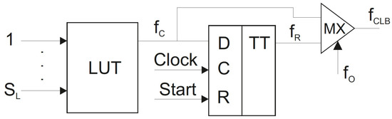
Figure 1.
Architecture of a look-up table (LUT)-based configurable logic block (CLB).
A LUT can implement a function dependent on up to arguments. A LUT is a combinational block. Thus, the value of could be changed by changing the values of arguments. Using the pulse of synchronization clock, the current value of is written into the D flip-flop. The output of flip-flop represents a registered function . The multiplexer selects an appropriate form of CLB’s output. The output is either combinational () or registered ().
An FSM circuit is represented by some SBF. For practical digital systems, an SBF can include around 50–70 literals [3,4]. However, a LUT has not more than six inputs. This limitation makes it necessary to transform SBFs representing FSM circuits. The transformation is executed using different methods of functional decomposition (FD) [32]. The FD-based transformation leads to FSM circuits with many levels of LUT-based CLBs and systems of unordered (irregular) interconnections. The functional decomposition leads to CLB-based circuits having “spaghetti-type” interconnections [33].
A Mealy FSM is represented as a six-component vector [34]. The vector S includes a set of inputs , a set of outputs , a set of internal states , a function of transitions , a function of output and an initial state . Various tools can be applied to represent the vector S. The most commonly used tools are: graph-schemes of algorithms [3,34], binary decision diagrams [35,36], state transition graphs [4] and inverter graphs [37]. In this article, we use state transition tables (STTs) to represent Mealy FSMs.
An STT includes the following columns [4]: a current state ; a state of transition (a next state) ; an input signal (it determines a transition from to ); a collection of outputs (it is generated during the transition from the current state into the next state). The column h includes the numbers of transitions (). For example, a Mealy FSM is represented by the STT (Table 1).

Table 1.
The state transition table (STT) of Mealy FSM .
As follows from Table 1, the FSM has two inputs, four outputs, three states and five transitions. From Table 1 we can find, for example, that and (these formulae follow from the first row of Table 1). The following steps should be executed to construct SBFs describing logic circuits of FSMs [3,34]: (1) the encoding of FSM states by binary codes ; (2) the constructing sets of state variables and input memory functions (IMFs) ; and (3) constructing a direct structure table (DST). To encode the states , the step of state assignment should be executed [2].
In this paper, we use the style of binary state assignment where the number state variables (R) is determined as
The binary state assignment is used, for example, in the system SIS [38]. The number of bits of the state code can vary from the minimum value determined by (1) to the number of states, M. If , then the corresponding state codes are one-hot codes. This style is used, for example, by the academic system ABC [37] of Berkeley.
A special state register () keeps FSM state codes. It is controlled by two internal pulses. The pulse start causes the loading of the initial state code into the . The pulse clock sets the time when the can be changed. For CLB-based FSMs, state registers are constructed on the basis of D flip-flops [2]. In this article, we also use state registers based on D flip-flops. The pulse clock allows the functions to change the content.
After the state assignment, each state is represented by its code . The Boolean systems representing an FSM circuit can be derived from a DST. Compared to the initial STT, a DST includes three additional columns: , and . The column includes the symbols corresponding to 1s in the code of the state from the row h of a DST. A DST is a base for finding the following SBFs:
The architecture of a Mealy FSM is defined by these systems of Boolean functions (SBFs). It is shown in Figure 2.
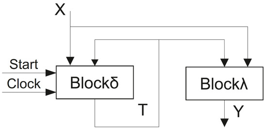
Figure 2.
Architecture of LUT-based Mealy FSM .
3. State-Of-The-Art
As a rule, the process of designing digital systems involves solving some optimization problems [2,4]. In the case of FPGA-based sequential blocks, these problems are the following [2,24]: (1) the reduction of chip resources required to implement a LUT-based circuit; (2) the decreasing the propagation time (the increasing the maximum operating frequency); and (3) the reducing power consumption. Our current article is devoted to improving the maximum operating frequency of LUT-based Mealy FSMs.
The characteristics of FPGA-based FSM circuits can be improved due to optimal state assignment [2,8,37,38,39,40,41,42]. Additionally, this can be done using embedded memory blocks (EMBs) instead of LUT-based CLBs [43,44,45,46,47,48,49,50]. Let us analyze these approaches.
We call optimal state codes such codes that allow reducing the numbers of arguments in SBFs (2) and (3). For example, the numbers of arguments is significantly reduced by the algorithm JEDI [38]. It is one of the best state assignments algorithms [2]. Due to it, we chose JEDI-based FSMs to compare with FSMs based on our proposed approach.
Modern industrial CAD tools include various state assignment strategies. For example, the following state assignment methods are used in the Xilinx design tool Vivado [40]: automatic state assignment (auto); sequential encoding; the one-hot; Gray encoding and Johnson codes. The same methods can be found in the package XST by Xilinx [51].
The one-hot state assignment is very popular in LUT-based design [41], because FPGAs include many programmable flip-flops. The one-hot state assignment leads to increasing the number of input memory functions compared with (1). However, these IMFs are much simpler than in the case of binary state assignment [2]. As follows from [41], it is better to use the one-hot codes if an FSM has more than 16 states. However, the characteristics of LUT-based FSM circuits significantly depend on the number of inputs [2]. As follows from [42], the binary state encoding allows producing better FSM circuits if . Since each approach is good under certain conditions, we compare both of these encoding styles with our proposed method. The method of binary state assignment auto of Vivado is used as a baseline for comparison with the proposed method.
To reduce the power consumption, it is very important to diminish the number of interconnections inside an FSM circuit. Therefore, to diminish the number of interconnections, it is necessary to minimize the numbers of arguments in SBFs (2) and (3) [2]. Thus, it is always useful to apply the optimal state assignment to improve the characteristics of FSM circuits.
The second approach to optimizing CLB-based FSMs is related to using EMBs instead of LUTs [47]. There are many design methods targeting EMB-based FSMs [47,48,49,52,53,54,55,56,57].The survey of different methods of EMB-based design can be found in [47]. In the best case, only a single EMB is necessary to implement an FSM circuit [49]. However, if the number of arguments in systems (2) and (3) exceeds the maximum possible number of EMB address inputs, then an FSM is represented by a network of EMBs. To diminish the number of EMBs in such a network, it is necessary to implement some functions using LUTs [2,49].
Thus, an FSM circuit can be implemented as either a network of EMBs, or a network of LUTs, or a joint network of LUTs and EMBs. In this article, we discuss the second case, when FSM circuits are implemented using LUT-based CLBs. This approach makes sense if: (1) all EMBs are used to implement other parts of a digital system or (2) the number of arguments in SBFs (2) and (3) exceeds 15 (this is a maximum possible number of modern EMBs [11,12,13]).
Denote as the number of literals [4] in sum-of-products (SOPs) of functions (2) and (3). If the condition
takes place, then a logic circuit for any function is represented by exactly one LUT. If , then the corresponding logic circuit can be obtained using various methods of FD [21,23,27,35,36,48,58,59]. The FD can be viewed as a process during which decomposed functions are broken down into smaller and smaller components. If any component depends on no more than arguments, the process of FD for a given function is completed. Of course, this results in multi-level LUT-based circuits. For these circuits, it is typical that the same inputs or state variables appear on several logic levels. It significantly complicates the system of interconnection between LUTs of FD-based FSM circuits (with all the ensuing consequences).
In the best case, the LUT count of an FSM circuit is equal to the total number of inputs and state variables. However, if the condition (4) is violated, the LUT count increases by the value of , where is a set of additional functions different from (2) and (3). These additional functions are components of functions (2) and (3) produced during the process of FD. We do not discuss these methods in our article.
The reducing LUT counts in circuits of Mealy FSMs can be achieved using the various methods of structural decomposition [7,39]. These methods eliminate a direct dependence of functions and on inputs . The methods of structural decomposition are also connected with introducing new functions . Functions depend on variables and . The structural decomposition allows reducing LUT counts if there is
These new functions are divided into subsystems having unique input and output variables. Each subsystem determines a separate LUT-based block of logic. When the condition (5) takes place, the total LUT count for a decomposed FSM is significantly less than it is for equivalent FSM . The new functions are arguments of functions (2) and (3). If the condition
takes place, then the total LUT count of a decomposed FSM circuit is significantly less than it is for an equivalent multi-level circuit . A survey of different methods of structural decomposition is represented in [7].
In this article, we discuss three known methods of structural decomposition [7,34]: replacement of inputs, encoding of outputs and transformation of codes of collections of outputs into state codes. Consider these approaches.
To reduce the LUT count, the inputs could be replaced by additional variables , where [34]. As a rule, the value of G is determined as [34]:
The system of additional variables is represented by the SBF
The functions are represented by the following SBFs:
Collections of outputs (COs) include functions generated simultaneously. To synthesize an FSM circuit, it is necessary to represent each CO by a binary code . As a rule, the number of bits in these codes is determined as
To create codes , it is necessary to use additional variables . This allows representing outputs of FSM as the following:
The additional variables are represented by the following system:
To generate functions (13), an additional block of logic should be used.
In the work [30], two known methods of structural decomposition are used for reducing LUT count for FPGA-based Mealy FSMs. It results in Mealy FSM shown in Figure 3.
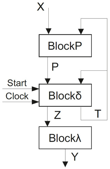
Figure 3.
Architecture of Mealy FSM .
The logic circuit of Mealy FSM has three logic levels. The executes the replacement of inputs by additional variables and implements the SBF (8). The generates input memory functions (9) and additional variables used for encoding of collections of outputs . This block includes a distributed register keeping state codes. To generate variables , it is necessary to implement the system
implements the system (12) dependent on additional variables .
As our investigations [30] show, this approach allows significantly reducing the LUT count as compared to equivalent FSM . However, this solution has a serious drawback: the performance of FSM is always less than it is for an equivalent Mealy FSM .
In [36], different models of Mealy FSMs based on transformation of object codes are discussed. One of the typical methods from this group is a transformation of codes into state codes .
The main idea of this approach is the following. For example, some CO is generated during transitions into states and . Using CO , it is possible to determine these states. To do it, it is necessary to use identifiers and . Using two pairs allows the following representation of these states of transition: and . Thus, each state can be represented by one or more pairs . To create the set of identifiers , it is necessary to find the maximum amount of pairs () including the same CO .
Each identifier is represented by a binary code having bits, where
To encode identifiers, the elements of the set are used.
It allows representing the IMFs by the following system:
The variables are represented by the following system:
Thus, an FSM based on this principle implements systems (12), (13), (16) and (17). It is an FSM shown in Figure 4.
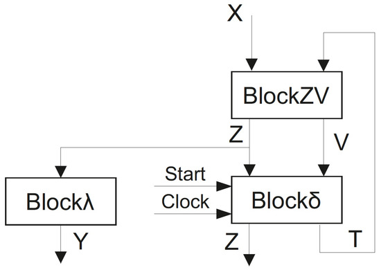
Figure 4.
Architecture of Mealy FSM .
In FSM , the implements systems (13) and (17); the implements input memory functions represented as (16); the implements the system (12). Thus, there are only two levels of logic between inputs and outputs in the case of FSM . As follows from Figure 3, there are three levels of logic between inputs and outputs in the case of FSM .
This property of FSM can be used for acceleration of a digital system. As is known [2], outputs (3) of Mealy FSM are not stable. If inputs are changing during a clock cycle, the outputs (3) may also change. This may cause the digital system as a whole to crash. To prevent failures, it is necessary to prohibit the access of incorrect outputs (3) to a digital system. To do it, a special register is introduced (Figure 5).
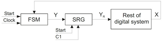
Figure 5.
Interaction of FSM with the rest of a digital system.
If all transients in the FSM circuit are completed and the values of outputs are stable, then a pulse of synchronization is generated. It allows loading outputs into . Next, the registered outputs enter the digital system. The system executes the corresponding operations and generates the values of inputs . Such an interaction should be organized for any model of Mealy FSM.
Thus, in the case of FSM , the pulse may be generated when the correct values are set for the outputs of two blocks ( and ). In the case of FSM , the correct outputs are set after all three blocks are triggered sequentially. Thus, the model can provide better performance than the model .
There is one very serious disadvantage of FSM compared to equivalent FSM . If the relation
is true, then the number of LUTs (and maybe their levels) in is significantly more than in of equivalent FSM . In this article, we propose a method which allows reducing the number of LUTs in FSM .
4. Main Idea of the Proposed Method
In this article, we discuss a case when the condition (4) is violated for some functions . It leads to a multi-level circuit of with an irregular system of interconnections. Obviously, it degenerates the performance of FSM . To diminish the number of levels of LUTs in the circuit of , we propose the following approach.
As it is in the case of two-fold state assignment [7,60], we propose to construct a partition of the set A such that the following condition takes place:
Using methods [7,60] allows creating the required partition having the minimum possible number of classes, J.
If a class includes states ,
then there are enough state variables to encode the states . To do it, the state variables are used. There are elements in the sets T and :
If , then for . It explains the presence of 1 in (20).
Now, we can encode each state by a code having bits. In this code, variables are equal to zero. Only variables identify a state as an element of .
As , the codes are extended state codes [7]. However, only state variables are used to represent functions dependent on states .
To find SBFs (13) and (17), it is necessary to construct a table of (). It includes the columns , , , , , , , , , and h.
A class determines a table which is a subtable of . A table determines sets , and . These variables are written in the columns , and of , respectively. Additionally, a table determines SBFs
Using this preliminary information, we propose an architecture of Mealy FSM (Figure 6).
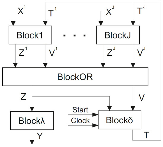
Figure 6.
Architecture of Mealy FSM .
implements functions and as disjunctions:
If , then there is only a single level of LUTs in the circuit of . Otherwise, it is a multi-level block.
and execute the same functions as these blocks in FSM . The generates functions (12), the the functions (16). If , then includes only a single level of LUTs.
Thus, in the best case, there are three levels of LUTs between inputs and outputs . If the condition (4) is violated for equivalent FSM , then the FSM provides higher operating frequency.
Comparison of Figure 4 and Figure 6 shows that: (1) of is replaced by Block1, …, , and (2) of has outputs. These two issues are the main specifics of FSM .
In this paper, we propose a method of synthesis of finite state machine . If an FSM is represented by an STT, then the method includes the following steps:
- Representing states by pairs .
- Encoding of collections of outputs and identifiers. Constructing SBF (12) representing .
- Constructing the partition of the set A.
- Creating tables determining Block1–.
- Constructing SBFs representing –.
- Constructing SBF (16) representing .
- Implementing the logic circuit of FSM .
The first step is executed using an initial STT. If CO is generated during transitions into different states , then there are identifiers. Each identifier determines an unique state represented by . The cardinality of the set is determined as
Step 2 is executed on the basis of STT. The COs should be encoded in a way optimizing the number of literals in SBF (12). Identifiers can be encoded in the trivial way.
The partition is constructed using methods from [7,43]. After finding classes , we can encode the states . It gives sets and .
A table of has the following columns: , , , , , h. The states are written in the column . As if , we can write only parts of created from state variables . A column includes variables , a column variables . The outcome of step 4 is tables of Block1–BlockJ.
A table is a base to derive the SBFs (24) and (25). The terms of corresponding SOPs are conjunctions , where is a conjunction of variables . All other state variables are treated as insignificant. The SBF (24) and (25) are used to implement circuits of Block1–BlockJ.
The step 6 is executed in the trivial way. If , then there is a single level of LUTs in BlockOR. In this case, its circuit includes exactly LUTs.
To find the SBF (16), it is necessary to construct a table of . This table includes the following columns: , , , , , , , h. Each row of this table corresponds to a pair determining the state . The terms of SOPs (16) are conjunctions of variables and . The corresponding literals are determined by codes and .
The last step is executed using standard CAD tools. It is based on program tools translating initial STT into required SBFs. These SBFs are used into VHDL models of FSMs.
Now, we would like to show the difference between the two-fold state assignment [60] and the proposed method. In the first case, there are two sets of state variables. The set is used to encode states as elements of set A. The set is used to encode states as elements of sets . Due to it, there are two levels of logic creating inputs of the Block1–BlockJ. In the proposed approach, the inputs of these block are generated by . Thus, the proposed approach leads to faster FSMs than for the two-fold state assignment.
5. Example of Synthesis
In this article, we use a symbol to show that an FSM model is used to synthesize an FSM . An example of synthesis of Mealy FSM is shown in this section. A Mealy FSM is represented by Table 2.
Table 2.
STT of Mealy FSM .
The following characteristics of follow from Table 2: the number of states , the number of transitions , the number of inputs and the number of outputs . Additionally, the following collections of outputs can be found from Table 2: , , , , , , . Thus, there is .
1. Representing states by pairs .
Using STT (Table 2), it is possible to find pairs representing the states . For example, the CO is written in the rows 1, 9, 12 and 13. Additionally, these rows include the states of transitions (rows 1 and 12) and (rows 9 and 13). Thus, it is necessary two identifiers (, ) to distinguish these states: , .
Using the same approach, we can find all pairs for the given example. The process is shown in Figure 7. Using (26) gives and .
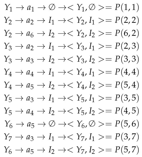
Figure 7.
Representation of states by pairs .
In the discussed case, there is , where is a number of pairs . Thus, the will be represented by the table having 12 rows.
2. Encoding of COs and identifiers . There is , . Using (11) gives and the set . Using (15) gives and the set .
There is . Therefore, each equation from SBF (16) is implemented using only a single look-up table. Thus, there is no need in encoding of COs in a way optimizing (16). Let us encode COs in a way optimizing the SBF (12).
Using contents of COs, the following SBF can be obtained:
To diminish the number of interconnections between and , it is necessary to reduce the number of literals in functions (12). It can be done using approach [61]. One of the possible solutions is shown in Figure 8.
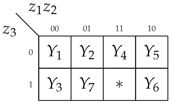
Figure 8.
Outcome of encoding of collections of outputs (COs).
Using codes from Figure 8 and rules of minimization [4], we can transform the SBF (27) into the following system:
The system (28) represents of . This block has 18 interconnections with . In the common case, there are literals (and 24 interconnections). Thus, the number of interconnections is reduced by 1.33 times thanks to encoding of COs shown in Figure 8.
The identifiers can be encoded in a trivial way: and . Now, the identifier is determined by , and by .
3. Constructing the partition of the set A. There is in the discussed example. It means that each block should satisfy the condition .
This step is very important because it determines significantly the characteristics of FSM [60]. We do not discuss this step in detail. Instead, we use the approach [60] to create the partition with classes and . Using Table 2 gives the sets and .
Using (20) gives , , , and . There is . It means that . Thus, the found partition satisfies the condition (19).
Due to it, state codes do not affect the number of look-up tables in circuits of Block1 and Block2. We can encode them in the following way: , , , , and .
4. Creating tables of Block1 and Block2. To do it, we should construct a table of of equivalent FSM . Next, this table is divided by two tables using classes and codes .
Table of is constructed using an initial STT. To do it, the states of transitions are replaced by corresponding pairs . Additionally, the codes , and columns , are introduced instead of the column of STT. In the discussed example, the is represented by Table 3.
Table 3.
Table of of Mealy FSM .
In Table 3, we used codes from Figure 8. The pairs <> were taken from Figure 7. To design circuits of Block1–BlockJ, Table 3 should be transformed into a set of tables representing blocks of the first level of logic.
Consider the row of Table 3. It corresponds the pair . Thus, the column includes and the column includes . The column includes , the column the code . It explains the contents of columns and of the row 1. The column is the same as for initial STT (Table 2). All other rows are filled in the same way.
To create tables of a Blockj, we should: (1) choose state and (2) take rows of table of BlockZV for these states. In this case, the Block1 is represented by Table 4 and the Block2 by Table 5. In Table 4 and Table 5 the superscripts 1 and 2 mean that corresponding functions are implemented by Block1 or Block2, respectively.
Table 4.
Table of Block1 of Mealy FSM .
Table 5.
Table of Block2 of Mealy FSM .
5. Constructing systems representing blocks of the first level. These systems are constructed using Table 4 and Table 5. Each system includes equations.
The Block1 is represented by the following SBF:
The Block2 is represented by the following SBF:
6. Constructing the system for BlockOR. This system is constructed in a trivial way. Each function is represented by a disjunction of functions of the same name with different upper indexes. It is the following SBF in the discussed case:
7. Constructing the system for . To find the system (16), it is necessary to create a table of . It is constructed using pairs and codes , and . In the discussed case, this is Table 6. The table uses data from Figure 7 and Figure 8. The following SBF is derived from Table 6:
Table 6.
Table of of Mealy FSM .
Now, we have systems for each block of FSM . Next step is the implementation of the logic circuit.
8. Implementing the logic circuit of FSM . This step is executed using special synthesis tools, e.g., Quartus Prime [50] or Vivado by Xilinx [40]. During this step, each LUT is represented by its truth table. Such complicated tasks are executed as mapping, placement and routing [6]. We just focus on finding the number of LUTs in the circuit and do not discuss this step for our example.
The Block1 is represented by the SBF (29). The corresponding circuit includes four LUTs. The Block2 is represented by the SBF (30). Its circuit also includes four LUTs. Thus, the first level of logic includes eight LUTs having .
The BlockOR is represented by the SBF (31). To implement its circuit, it is enough to have four LUTs. is represented by the SBF (28). Its circuit consist of 8 LUTs. At last, the system (32) represents . Its circuit has four LUTs.
Thus, the circuit of FSM includes 24 LUTs. There are three levels of LUTs between inputs and outputs . The same is true for inputs and input memory functions .
This example is very simple. We show it to explain all steps of the proposed method. The next Section shows results of experiments with more complex FSMs.
6. Experimental Results
In this section we show the results of experiments based on benchmark FSMs from the library [31]. There are 48 benchmarks in the library. They are very often used to compare outcomes of different design methods. The benchmark Mealy FSMs are represented in the format KISS2. We do not show the characteristics of these benchmarks in this article. They can be found, for example, in [30].
To implement FPGA-based FSM, we used VHDL-based FSM models. Our CAD tool K2F [2] translated the benchmarks into VHDL-based FSM models. The synthesis and simulation of FSMs were executed by the Active-HDL environment. As a target platform, we used Xilinx VC709 Evaluation Board (Virtex 7, XC7VX690T-2FFG1761C) [62]. This chip includes LUTs having . To execute the technology mapping and produce reports with characteristics of resulting FSM circuits, we used Xilinx CAD tool Vivado—version 2019.1 [40].
When we investigated FSM [30], we found that this model allows producing circuits with less area and power consumption if . In [30], we divided the benchmarks into five groups using the values of and . If , then benchmarks belong to group 0 (trivial FSMs); if , then to group 1 (simple FSMs); if , then to group 2 (average FSMs); if , then to group 3 (big FSMs); otherwise, they belong to group 4 (very big FSMs). As our research [30] shows, the larger the group number, the bigger the gain from using our method. We use the same division of benchmarks in this article too.
Group 0 includes the following benchmarks: bbtas, dk17, dk27, dk512, ex3, ex5, lion, lion9, mc, modulo12 and shiftreg. Group 1 contains the most benchmarks. They are the following: bbara, bbsse, beecount, cse, dk14, dk15, dk16, donfile, ex2, ex4, ex6, ex7, keyb, mark1, opus, s27, s386, s840 and sse. Group 2 consists of the following 12 benchmarks: ex1, kirkman, planet, planet1, pma, s1, s1488, s1494, s1a, s208, styr and tma. There is only a single benchmark: sand in Group 3. Group 4 includes the following benchmarks: s420, s510, s820 and s832.
In the section State-of-the-art, we have justified the choice of three methods for comparison with our approach. We chose the method auto of Vivado as a method based on binary state codes. Additionally, we used the method one-hot of Vivado. Due to its high reputation, we chose JEDI-based FSMs as a basis for comparison too. Our approach is a competitor to the method from work [30]. Thus, we chose -based FSMs with three levels of logic blocks as the fourth method used in experiments. The results of experiments are shown in Table 7 (the number of LUTs) and Table 8 (the maximum operating frequency). These results were taken from reports generated by Vivado.
Table 7.
Results of experiments (LUT count).
Table 8.
Results of experiments (the operating frequency, MHz).
We use the same organization of Table 7 and Table 8. Their rows are marked by the names of benchmarks, the columns by investigated design methods. The row “Total” includes results of summation for corresponding values. The summarized characteristics of our approach (-based FSMs) were taken as 100%. The row “Percentage” shows the percentages of summarized characteristics of FSM circuits implemented by other methods, respectively, compared to benchmarks based on our approach. Let us point out that the model was used for designs with auto, one-hot, and JEDI.
As follows from Table 7, the -based FSMs require fewer LUTs than other investigated methods. Our approach produces circuits having 8.84% more LUTs than equivalent -based FSMs. However, our approach requires fewer LUTs than auto (24.86% of gain), one-hot (45.3% of gain) and JEDI-based FSMs (2.83% of gain). The higher is the group, the greater is the gain in LUTs respectively auto, one-hot and JEDI-based FSMs. We show these results in Figure 9.
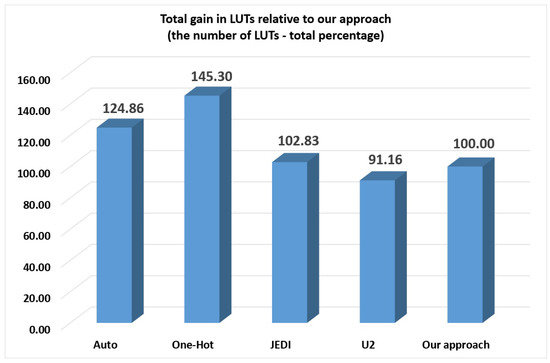
Figure 9.
Total gain in LUTs relative to our approach (LUT count—total percentage).
Analysis of Table 8 shows that the -based FSMs have the highest operating frequency of the investigated methods. Our method gives us a 9.85% advantage over the auto. The one-hot of Vivado loses 10.48% to our approach. The -based FSMs provide a 3.18% gain compared to JEDI-based FSMs. At last, the -based FSMs have an average frequency of 12.57% less than it is for FSM based on our approach. These results are shown in Figure 10.
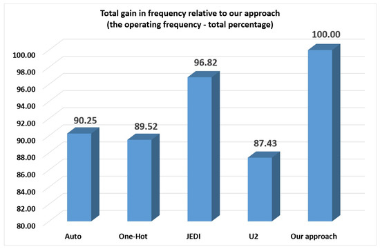
Figure 10.
Total gain in frequency relative to our approach (the operating frequency—total percentage).
To clarify how the gain in LUTs depends on the FSM group, we have created Table 9 (gain in LUTs for group 0), Table 10 (gain in LUTs for group 1) and Table 11 (gain in LUTs for groups 2–4). Additionally, we present these results by graphs on Figure 11, Figure 12 and Figure 13, respectively. To clarify how the gain in frequency depends on the FSM group, we have created Table 12 (gain in frequency for group 0), Table 13 (gain in frequency for group 1) and Table 14 (gain in frequency for groups 2–4). Additionally, we present these results by graphs on Figure 14, Figure 15 and Figure 16, respectively.
Table 9.
Gain in LUTs for group 0 (LUT count).
Table 10.
Gain in LUTs for group 1 (LUT count).
Table 11.
Gain in LUTs for groups 2–4 (LUT count).
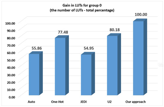
Figure 11.
Gain in LUTs for group 0 (LUT count—total percentage).
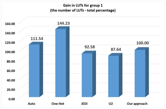
Figure 12.
Gain in LUTs for group 1 (LUT count—total percentage).
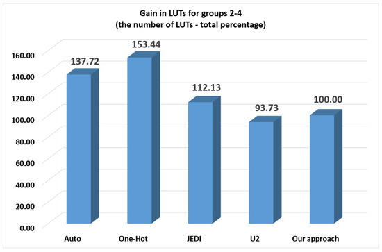
Figure 13.
Gain in LUTs for groups 2–4 (LUT count—total percentage).
Table 12.
Gain in frequency for group 0 (the operating frequency).
Table 13.
Gain in frequency for group 1 (the operating frequency).
Table 14.
Gain in frequency for groups 2–4 (the operating frequency).
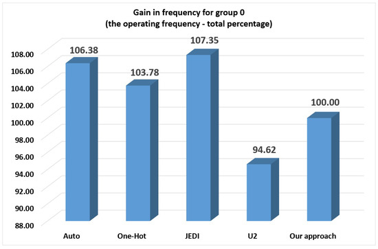
Figure 14.
Gain in frequency for group 0 (the operating frequency—total percentage).
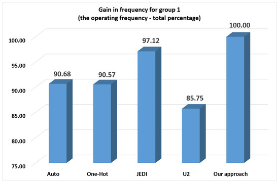
Figure 15.
Gain in frequency for group 1 (the operating frequency—total percentage).
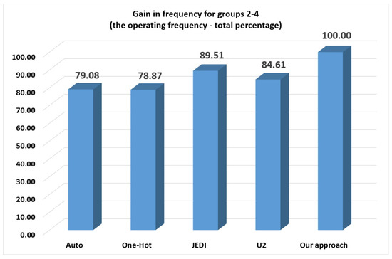
Figure 16.
Gain in frequency for groups 2–4 (the operating frequency—total percentage).
Analysis of Table 9 and Figure 10 shows that the -based FSMs have more used LUTs than other investigated methods. Our method has the following loss: 44.14% compared to auto, 22.52% compared to one-hot, 45.05% compared to JEDI-based FSMs and 19.82% compared to -based FSMs. Thus, this method is not suitable for small FSMs.
As follows from Table 10 and Figure 12, the -based FSMs of group 1 required fewer LUTs than FSMs based on auto (11.54% of gain) and one-hot (44.23% of gain). However, we still lose to the JEDI-based FSMs (7.42% of loss) and -based FSMs (12.36% of loss). Note that the loss decreased in comparison with the group 0.
As follows from Table 11 and Figure 10, the -based FSMs of groups 2–4 required fewer LUTs than FSMs based on auto (37.72% of gain), one-hot (53.44% of gain) and JEDI-based FSMs (12.13% of gain). Only -based FSMs have better results and our approach has 6.27% of loss. Note that the loss decreased in comparison with the group 1. Thus, starting from average FSMs, our approach loses only to the -based FSMs.
As follows from Table 12 and Figure 14, the -based FSMs of group 0 are faster than -based FSMs (5.38% of gain). In this group, the best results belong to JEDI-based FSMs. They have the following gains: (1) 0.9% regarding auto; (2) 3.57% regarding one-hot; (3) 12.73% regarding -based FSMs; (4) 7.35% regarding our approach. Thus, for the group 0, there is no sense in applying our approach. However, starting from the group 1, our method allows producing faster circuits than the other investigated methods.
The proposed approach produces the best results for FSMs from group 1 (Table 13 and Figure 15). There are the following gains: (1) 9.32% regarding auto; (2) 9.43% regarding one-hot; (3) 2.88% regarding JEDI-based FSMs; and (4) 14.25% regarding -based FSMs. Our approach provides even better results (Table 14 and Figure 16) for FSMs from groups 2–4. The gain increases and amounts to: (1) 20.92% regarding auto; (2) 21.13% regarding one-hot; (3) 10.49% regarding JEDI-based FSMs; and (4) 15.39% regarding -based FSMs.
As can be seen from Table 8, the -based FSMs require fewer LUTs compared to other methods. Analysis of Table 9 shows that -based FSMs are the ones with the highest maximum operating frequency compared to other methods. The overall design quality can be estimated by the product of used resources [63] (for example, chip area occupied by a circuit) and the latency time. As it is in [63], we use the number of LUTs to compare areas required for FSM circuits based on different models (auto, one-hot, JEDI, and ). As a rule, an FSM is only a part of a digital system. We do not know how many cycles a system needs to perform a required task. Thus, we cannot find absolute values of latency times. However, for a relative evaluation of different models, it is sufficient to know only the time of cycle.
In this article, we have performed a generalized comparison of the models used in experiments. As a generalized assessment, we used the result of multiplying the number of LUTs in an FSM circuit by the cycle time. The numbers of LUTs are taken from Table 7. To calculate the cycle times in nanoseconds, we used the operating frequencies from Table 8. The area-time products measured in × are shown in Table 16.
To better evaluate the chip resources used by FSM circuits, we have created Table 15. It contains the numbers of flip-flops required for implementing the state registers. As follows from Table 15, there are the same number of flip-flops in registers of FSMs obtained using methods auto, JEDI and -based FSMs. For these FSMs the number of memory elements is the same. They use the least number of flip-flops determined as . The largest number of flip-flops is consumed by FSMs based on the one-hot state assignment (eight times more than, for example, -based FSMs and 4.97 times more than -based FSMs). Our approach gives a gain of 397% compared to one-hot-based FSMs, but loses 37% to other investigated methods. If we find the difference between, for example, the number of flip-flops in registers of - and -based FSMs, we can see that the difference decreases as the group number decreases.
Table 15.
Results of experiments (FFs count).
As follows from Table 16, our approach produces FSM circuits with better area-time products than those of other investigated methods. Our approach gives the following gains: (1) 55.24% regarding auto; (2) 79.87% regarding one-hot; (3) 12.28% regarding JEDI-based FSMs; and (4) 8.6% regarding -based FSMs. If we compare results for different groups, we can draw the following conclusions. Our approach loses out to all other models for group 0. For group 1, -based FSMs lose out only to JEDI-based FSMs (4.46% of loss). However, our approach provides significantly better area-time products for FSMs from groups 2–4. In this case, our approach gives the following gains: (1) 76.79% regarding auto; (2) 97.55% regarding one-hot; (3) 24.71% regarding JEDI-based FSMs; and (4) 12.63% regarding -based FSMs.
Table 16.
Results of experiments (the generalized assessments, ).
The results of our experiments show that the proposed approach can be used instead of other models starting from simple FSMs. The -based FSMs have fewer LUTs than other models. However, starting from average FSMs, our approach allows producing circuits having slightly larger numbers of LUTs with significantly higher maximum operating frequencies. Additionally, our approach provides better area-time products starting from average FSMs. It has rather good potential and can be used in targeting FPGA-based Mealy FSMs.
7. Conclusions
Modern FPGA chips have reached such a level that quite complex systems can be implemented using only a single chip. At the same time, significant parts of the digital systems are implemented using LUTs having rather small numbers of inputs. The value is considered as optimal [19,20], but it is too small compared to the number of inputs and outputs of FSMs from modern digital systems. To design these complex FSMs with the use of such simple elements, it is necessary to apply the methods of functional decomposition. As a rule, the functional decomposition results in LUT-based FSM circuits having many logic levels and very complicated systems of interconnections.
Different methods of structural decomposition can be used to optimize the characteristics of FPGA-based FSM circuits. Our research [30,60] shows that the FSM circuits based on structural decomposition possess significantly better characteristics (fewer LUTs, higher maximum operating frequency, lower power consumption) than their counterparts based on functional decomposition. It is very important that the FSM circuits based on structural decomposition have regular systems of interconnections and predicted numbers of levels of logic. In the best case, each logic block of an FSM circuit has only a single level of LUTs.
In this paper, we propose a novel approach aimed at optimization of LUT-based Mealy FSMs. The proposed method leads to Mealy FSM . Two methods of structural decomposition are the cornerstones of our approach. They are: (1) the transformation of codes of collections of outputs into state codes and (2) the extension of state codes. The second method is a new one and it is proposed in this paper. To increase the maximum operating frequency, we encode the FSM states using more than the minimum number of state variables determined by (1). Our approach leads to Mealy FSM circuits with three levels of LUTs and regular systems of interconnections. As it is in a single-level FSMs , FSM outputs are generated simultaneously with input memory functions. As a result, our approach provides an increase in maximum operating frequency, accompanied by a small increase in the number of LUTs compared to equivalent three-level FSMs.
The results of our experiments clearly show that the proposed approach can be used instead of other models starting from simple FSMs. The -based FSMs have fewer LUTs than other models. However, starting from average FSMs, our approach allows producing circuits having slightly larger numbers of LUTs with significantly higher maximum operating frequency. Additionally, our approach provides better area-time products starting from average FSMs. Thus, our approach can be used if either the performance or the area-time product is the dominant characteristic of a digital system.
We are currently considering several areas of research. We intend to explore the possibility of applying the proposed approach to FPGA chips of Intel (Altera). We will also try to adapt this approach for optimizing characteristics of Moore finite state machines.
Author Contributions
Conceptualization, A.B., L.T. and K.K.; methodology, A.B., L.T., K.K. and S.S.; software, A.B., L.T. and K.K.; validation, A.B., L.T. and K.K.; formal analysis, A.B., L.T., K.K. and S.S.; investigation, A.B., L.T. and K.K.; writing—original draft preparation, A.B., L.T., K.K. and S.S.; supervision, A.B. All authors have read and agreed to the published version of the manuscript.
Funding
This research received no external funding.
Conflicts of Interest
The authors declare no conflict of interest.
Abbreviations
The following abbreviations are used in this manuscript:
| BIMF | block of input memory functions |
| CLB | configurable logic block |
| COF | collection of output functions |
| CO | collection of output |
| DST | direct structure table |
| EMB | embedded memory block |
| FD | functional decomposition |
| FSM | finite state machine |
| FPGA | field-programmable gate array |
| LUT | look-up table |
| SBF | systems of Boolean functions |
| SOP | sum-of-products |
| STT | state transition table |
References
- Bailliul, J.; Samad, T. (Eds.) Encyclopaedia of Systems and Control; Springer: London, UK, 2015; p. 1554. [Google Scholar]
- Sklyarov, V.; Skliarova, I.; Barkalov, A.; Titarenko, L. Synthesis and Optimization of FPGA-Based Systems; Volume 294 of Lecture Notes in Electrical Engineering; Springer: Berlin, Germany, 2014. [Google Scholar]
- Baranov, S. Logic and System Design of Digital Systems; TUTPress: Tallinn, Estonia, 2008. [Google Scholar]
- Micheli, G.D. Synthesis and Optimization of Digital Circuits; McGraw-Hill: Cambridge, MA, USA, 1994. [Google Scholar]
- Minns, P.; Elliot, I. FSM-Based Digital Design Using Verilog HDL; JohnWiley and Sons: Hoboken, NJ, USA, 2008. [Google Scholar]
- Grout, I. Digital Systems Design with FPGAs and CPLDs; Elsevier Science: Amsterdam, The Netherlands, 2011. [Google Scholar]
- Barkalov, A.; Titarenko, L.; Mielcarek, K.; Chmielewski, S. Logic Synthesis for FPGA-Based Control Units—Structural Decomposition in Logic Design; Volume 636 of Lecture Notes in Electrical Engineering; Springer: Berlin/Heidelberg, Germany, 2020. [Google Scholar]
- Gajski, D.D.; Abdi, S.; Gerstlauer, A.; Schirner, G. Embedded System Design: Modeling, Synthesis and Verification; Springer Science & Business Media: Berlin/Heidelberg, Germany, 2009. [Google Scholar]
- Krzywicki, K.; Barkalov, A.; Andrzejewski, G.; Titarenko, L.; Kolopienczyk, M. SoC research and development platform for distributed embedded systems. Przegląd Elektrotechniczny 2016, 92, 262–265. [Google Scholar] [CrossRef][Green Version]
- Czerwinski, R.; Kania, D. Finite State Machine Logic Synthesis for Complex Programmable Logic Devices; Volume 231 of Lecture Notes in Electrical Engineering; Springer: Berlin/Heidelberg, Germany, 2013. [Google Scholar]
- Intel FPGAs and Programmable Devices. Available online: https://www.intel.pl/content/www/pl/pl/products/programmable.html (accessed on 9 September 2020).
- Altera. Cyclone IV Device Handbook. Available online: http://www.altera.com/literature/hb/cyclone-iv/cyclone4-handbook.pdf (accessed on 9 September 2020).
- Xilinx FPGAs. Available online: https://www.xilinx.com/products/silicon-devices/fpga.html (accessed on 9 September 2020).
- Sass, R.; Schmidt, A. Embedded System Design with Platform FPGAs: Principles and Practices; Morgan Kaufmann Publishers: Amsterdam, The Netherlands, 2010; p. 409. [Google Scholar]
- Branco, S.; Ferreira, A.G.; Cabral, J. Machine Learning in Resource-Scarce Embedded Systems, FPGAs, and End-Devices: A Survey. Electronics 2019, 8, 1289. [Google Scholar] [CrossRef]
- Cheng, Q.; Zhao, X.; Wen, M.; Shen, J.; Tang, M.; Zhang, C. SAPTM: Towards High-Throughput Per-Flow Traffic Measurement with a Systolic Array-Like Architecture on FPGA. Electronics 2020, 9, 1160. [Google Scholar] [CrossRef]
- Wang, Z.; Tang, Q.; Guo, B.; Wei, J.-B.; Wang, L. Resource Partitioning and Application Scheduling with Module Merging on Dynamically and Partially Reconfigurable FPGAs. Electronics 2020, 9, 1461. [Google Scholar] [CrossRef]
- Salauyou, V.; Ostapczuk, M. State Assignment of Finite-State Machines by Using the Values of Output Variables. In Theory and Applications of Dependable Computer Systems. DepCoS-RELCOMEX 2020. Advances in Intelligent Systems and Computing; Zamojski, W., Mazurkiewicz, J., Sugier, J., Walkowiak, T., Kacprzyk, J., Eds.; Springer: Cham, Switzerland, 2020; Volume 1173, pp. 543–553. [Google Scholar]
- Kilts, S. Advanced FPGA Design: Architecture, Implementation, and Optimization; Wiley-IEEE Press: Hoboken, NJ, USA, 2007. [Google Scholar]
- Kuon, I.; Tessier, R.; Rose, J. FPGA architecture: Survey and challenges—found trends. Electr. Des. Autom. 2008, 2, 135–253. [Google Scholar]
- Scholl, C. Functional Decomposition with Application to FPGA Synthesis; Kluwer Academic Publishers: Boston, MA, USA, 2001. [Google Scholar]
- Kubica, M.; Kania, D. Technology mapping oriented to adaptive logic modules. Bull. Pol. Acad. Sci. 2019, 67, 947–956. [Google Scholar]
- Kubica, M.; Kania, D. Decomposition of multi-level functions oriented to configurability of logic blocks. Bull. Pol. Acad. Sci. 2017, 67, 317–331. [Google Scholar]
- Mishchenko, A.; Chattarejee, S.; Brayton, R. Improvements to technology mapping for LUT-based FPGAs. IEEE Trans. CAD 2006, 27, 240–253. [Google Scholar]
- Kubica, M.; Kania, D.; Kulisz, J. A technology mapping of fsms based on a graph of excitations and outputs. IEEE Access 2019, 7, 16123–16131. [Google Scholar] [CrossRef]
- Kubica, M.; Kania, D. Area-oriented technologymapping for lut-based logic blocks. Int. J. Appl. Math. Comput. Sci. 2017, 27, 207–222. [Google Scholar] [CrossRef]
- Machado, L.; Cortadella, J. Support-Reducing Decomposition for FPGA Mapping. IEEE Trans. Comput. Aided Des. Integr. Circuits Syst. 2020, 39, 213–224. [Google Scholar] [CrossRef]
- Mishchenko, A.; Brayton, R.; Jiang, J.-H.R.; Jang, S. Scalable don’t-care-based logic optimization and resynthesis. ACM Trans. Reconfigurable Technol. Syst. 2011, 4, 4. [Google Scholar] [CrossRef]
- Feng, W.; Greene, J.; Mishchenko, A. Improving FPGA Performance with a S44 LUT structure. In Proceedings of the 2018 ACM/SIGDA International Symposium on Field-Programmable Gate Arrays (FPGA”18), Monterey, CA, USA, 25–27 February 2018; p. 6. [Google Scholar] [CrossRef]
- Barkalov, A.; Titarenko, L.; Krzywicki, K. Reducing LUT Count for FPGA-Based Mealy FSMs. Appl. Sci. 2020, 10, 5115. [Google Scholar] [CrossRef]
- McElvain, K. LGSynth93 Benchmark; Mentor Graphics: Wilsonville, OR, USA, 1993. [Google Scholar]
- Rawski, M.; Łuba, T.; Jachna, Z.; Tomaszewicz, P. The Influence of Functional Decomposition Onmodern Digital Design Process. In Design of Embedded Control Systems; Springer: Boston, MA, USA, 2005; pp. 193–203. [Google Scholar]
- Dahl, O.; Dijkstra, E.; Hoare, C. (Eds.) Structured Programming; Academic Press: London, UK, 1972; p. 234. [Google Scholar]
- Baranov, S. Logic Synthesis of Control Automata; Kluwer Academic Publishers: Dordrecht, The Netherlands, 1994. [Google Scholar]
- Opara, A.; Kubica, M.; Kania, D. Strategy of Logic Synthesis using MTBDD dedicated to FPGA. Integr. VLSI J. 2018, 62, 142–158. [Google Scholar] [CrossRef]
- Kubica, M.; Opara, A.; Kania, D. Logic synthesis for FPGAs based on cutting of BDD. Microprocess. Microsyst. 2017, 52, 173–187. [Google Scholar] [CrossRef]
- Brayton, R.; Mishchenko, A. ABC: An Academic Industrial-Strength Verification Tool. In Computer Aided Verification (Berlin, Heidelberg, 2010); Touili, T., Cook, B., Jackson, P., Eds.; Springer: Berlin/Heidelberg, Germany, 2010; pp. 24–40. [Google Scholar]
- Sentowich, E.; Singh, K.; Lavango, L.; Moon, C.; Murgai, R.; Saldanha, A.; Savoj, H.; Stephan, P.R.; Bryton, R.; Sangiovanni-Vincentelli, A. SIS: A System for Sequential Circuit Synthesis; University of California: Berkely, CA, USA, 1992. [Google Scholar]
- Barkalov, A.; Titarenko, L.; Barkalov, A., Jr. Structural decomposition as a tool for the optimization of an FPGA-based implementation of a Mealy FSM. Cybern. Syst. Anal. 2012, 48, 313–322. [Google Scholar] [CrossRef]
- Vivado Design Suite User Guide: Synthesis. UG901 (v2019.1). Available online: https://www.xilinx.com/support/documentation/sw_manuals/xilinx2019_1/ug901-vivado-synthesis.pdf (accessed on 9 September 2020).
- De Micheli, G.; Brayton, R.K.; Sangiovanni-Vincentelli, A. Optimal state assignment for finite statemachines. IEEE Trans. Comput. Aided Des. Integr. Circuits Syst. 2006, 4, 269–285. [Google Scholar] [CrossRef]
- Sutter, G.; Todorovich, E.; López-Buedo, S.; Boemo, E. Low-power FSMs in FPGA: Encoding alternatives. In Integrated Circuit Design, Power and Timing Modeling, Optimization and Simulation; Springer: Berlin/Heidelberg, Germany, 2002; pp. 363–370. [Google Scholar]
- Klimovich, A.S.; Solovev, V.V. Minimization of mealy finite-state machines by internal states gluing. J. Comput. Syst. Sci. Int. 2012, 51, 244–255. [Google Scholar] [CrossRef]
- Zając, W.; Andrzejewski, G.; Krzywicki, K.; Królikowski, T. Finite State Machine Based Modelling of Discrete Control Algorithm in LAD Diagram Language With Use of New Generation Engineering Software. Procedia Comput. Sci. 2019, 159, 2560–2569. [Google Scholar] [CrossRef]
- El-Maleh, A.H. A probabilistic pairwise swap search state assignment algorithm for sequential circuit optimization. Integr. VLSI J. 2017, 56, 32–43. [Google Scholar] [CrossRef]
- Park, S.; Cho, S.; Yang, S.; Ciesielski, M. A new state assignment technique for testing and low power. In Proceedings of the 41st annual Design Automation Conference (2004), San Diego, CA, USA, 7–11 June 2004; pp. 510–513. [Google Scholar]
- Garcia-Vargas, I.; Senhadji-Navarro, R. Finite state machines with input multiplexing: A performance study. IEEE Trans. Comput. Aided Des. Integr. Circuits Syst. 2015, 34, 867–871. [Google Scholar] [CrossRef]
- Rawski, M.; Selvaraj, H.; Łuba, T. An application of functional decomposition in ROM-based FSM implementation in FPGA devices. J. Syst. Archit. 2005, 51, 423–434. [Google Scholar] [CrossRef]
- Kołopienczyk, M.; Titarenko, L.; Barkalov, A. Design of emb-based moore fsms. J. Circuits Syst. Comput. 2017, 26, 1–23. [Google Scholar] [CrossRef]
- Quartus Prime. Available online: https://www.intel.pl/content/www/pl/pl/software/programmable/quartus-prime/overview.html (accessed on 9 September 2020).
- Xilinx. XST UserGuide. V.11.3. Available online: https://www.xilinx.com/support/documentation/sw_manuals/xilinx11/xst.pdf (accessed on 9 September 2020).
- Rafla, N.I.; Gauba, I. A reconfigurable pattern matching hardware implementation using on-chip RAM-based FSM. In Proceedings of the 53rd IEEE International Midwest Symposium on Circuits and Systems, Seattle, WA, USA, 1–4 August 2010; pp. 49–52. [Google Scholar]
- Senhadji-Navarro, R.; Garcia-Vargas, I.; Jiménez-Moreno, G.; Civit-Balcells, A.; Guerra-Gutierrez, P. ROM based FSM implementation using input multiplexing in FPGA devices. Electron. Lett. 2004, 40, 1249–1251. [Google Scholar] [CrossRef]
- Garcia-Vargas, I.; Senhadji-Navarro, R.; Jiménez-Moreno, G.; Civit-Balcells, A.; Guerra-Gutierrez, P. ROM-based finite state machine implementation in low cost FPGAs. In Proceedings of the IEEE International Symposium on Industrial Electronics ISIE 2007, Vigo, Spain, 4–7 June 2007; pp. 2342–2347. [Google Scholar]
- Senhadji-Navaro, R.; Garcia-Vargas, I. High-Speed and Area-Efficient Reconfigurable Multiplexer Bank for RAM-Based Finite State Machine Implementations. J. Circuits Syst. Comput. 2015, 24, 7. [Google Scholar] [CrossRef]
- Barkalov, A.; Titarenko, L.; Mazurkiewicz, M.; Krzywicki, K. Encoding of terms in EMB-based Mealy FSMs. Appl. Sci. 2020, 10, 2762. [Google Scholar] [CrossRef]
- Senhadji, N.; Garcia-Vargas, I. High-Performance Architecture for Binary-Tree-Based Finite State Machines. IEEE Trans. Comput. Aided Des. Integr. Circuits Syst. 2018, 37, 796–805. [Google Scholar] [CrossRef]
- Selvaraj, H.; Nowicka, M.; Luba, T. Non-Disjoint Decomposition Strategy in Decomposition-Based Algorithms & Tools. In Proceedings of the International Conference on Computational Intelligence and Multimedia Application, Gippsland, Australia, 2 July–2 October 1998; pp. 34–42. [Google Scholar]
- Michalski, T.; Kokosiński, Z. Functional decomposition of combinational logic circuits with PKmin. Czas. Tech. 2016, 2016, 191–202. [Google Scholar]
- Barkalov, O.; Titarenko, L.; Mielcarek, K. Hardware reduction for LUT-based Mealy FSMs. Int. J. Appl. Math. Comput. Sci. 2018, 28, 595–607. [Google Scholar] [CrossRef]
- Achasova, S. Synthesis Algorithms for Automata with PLAs; Soviet Radio: Moscow, Russia, 1987. [Google Scholar]
- VC709 Evaluation Board for the Virtex-7 FPGA User Guide; UG887 (v1.6); Xilinx, Inc.: San Jose, CA, USA, 2019.
- Islam, M.M.; Hossain, M.S.; Shahjalal, M.D.; Hasan, M.K.; Jang, Y.M. Area-Time Efficient Hardware Implementation of Modular Multiplication for Elliptic Curve Cryptography. IEEE Access 2020, 8, 73898–73906. [Google Scholar] [CrossRef]
Publisher’s Note: MDPI stays neutral with regard to jurisdictional claims in published maps and institutional affiliations. |
© 2020 by the authors. Licensee MDPI, Basel, Switzerland. This article is an open access article distributed under the terms and conditions of the Creative Commons Attribution (CC BY) license (http://creativecommons.org/licenses/by/4.0/).