Abstract
Lead halide perovskites possess outstanding optical characteristics that can be employed in the fabrication of phototransistors. However, due to low current modulation at room temperature, sensitivity to the ambient environment, lack of patterning techniques and low carrier mobility of polycrystalline form, investigation in perovskite phototransistors has been limited to rigid substrates such as silicon and glass to improve the film quality. Here, we report on room temperature current modulation in a methylammonium lead iodide perovskite (MAPbI3) flexible transistor made by an extremely cheap and facile fabrication process. The proposed phototransistor has the top-gate configuration with a lateral drain–channel–source structure. The device performed in the linear and saturation regions both in the dark and under white light in different current ranges according to the illumination conditions. The transistor showed p-type transport characteristics and the field effect mobility of the device was calculated to be ~1.7 cm2 V−1 s−1. This study is expected to contribute to the development of MAPbI3 flexible phototransistors.
1. Introduction
Advanced applications of transistors for portable and wearable devices require the use of lightweight flexible substrates. Different technologies and materials have been employed to develop flexible phototransistors by low-temperature fabrication methods [1]. Among the materials that are compatible with low-temperature processes, organic semiconductors suffer from low mobility [2] and metal oxide semiconductors require complicated and costly deposition techniques for producing high quality films [3].
An excellent candidate to be used as the photoactive layer in phototransistors is metal halide perovskite. Over the past ten years, metal halide perovskites, and particularly MAPbI3, have been recognized as the fastest growing technology in solar cell applications. The widespread research into MAPbI3 photovoltaics is due to its outstanding optical properties, including a high absorption coefficient [4] and low intrinsic recombination rate [5], along with low-cost solution-based fabrication methods [6].
MAPbI3 is a semiconductor with a direct bandgap of about 1.55–1.65 eV [7], suitable for visible light absorption. MAPbI3 in its single crystal form has a mobility higher than 100 cm2V−1s−1 [8]. Although many efforts have been devoted to the fabrication of MAPbI3-based solar cells [9] and light emitting diodes (LEDs) [10], MAPbI3 photo-transistors are still immature [11].
The feasibility of making MAPbI3-based transistors has shown before [10,12,13,14,15,16,17,18,19,20,21,22,23,24,25,26,27]. Most of the fabricated devices used a Si wafer and a layer of SiO2 as the gate and the dielectric layer to make a bottom-gate transistor [13,17]. Spin coating of MAPbI3 on the gate dielectric results in a polycrystalline layer that presents the triode and saturation current–voltage (I–V) response in the transistor only at low temperatures (<200 K) [10,21]. The poor field effect in the devices operated at room temperature is likely due to the weak bonds between the cations and iodide anion that would generate defects in the semiconductor under an external biasing [10]. The weak bonds also affect the stability of MAPbI3 and result in hysteresis loops in the I–V characteristic [10]. Three approaches have been followed to obtain room temperature operation. A common approach is to mix MAPbI3 with an organic semiconductor, graphene, or carbon nanotube (CNT) to make hybrid semiconductors [13,17,25]. This method sacrifices the excellent optical absorption and low recombination rate in pure perovskites. In another approach, dual halide perovskites of MAPbBrαI(3-α) or MAPbClαI(3-α) were used instead of MAPbI3 to make more stable devices [28,29]. However, our earlier studies show that the photoelectric response of dual halide perovskites is much weaker than MAPbI3 [30]. Another approach to achieve higher stability is to make transistors from single crystals of MAPbI3 [26]. In this work, we have developed a new fabrication method that has previously tested for making perovskite-based photoresistors with no hysteresis effect and high stability of the device at room temperature [30,31,32,33].
In the new fabrication method, instead of using a thin-film design, a laser engraving method is applied to first make a microchannel across two conductive electrodes that later became the drain and source contacts. The microchannel was filled with a solution containing the perovskite precursors. The sample was dried to get a polycrystalline of MAPbI3. We have found that leaving the sample in vacuum for at least 24 h before coating the perovskite with a layer of a dielectric (i.e., CYTOP) improves the stability of the device significantly [33]. In this work, we used the CYTOP layer as the gate dielectric to make the transistor. Fabricating the device on a polyethylene terephthalate (PET) substrate, the final photodetector was mechanically flexible. The results of the studied device in this work is promising for further investigation of flexible sensors.
2. Materials and Methods
Perovskite precursor was prepared by mixing 0.5 M PbI2 (98.5%, Alfa Aesar, Haverhill, MA, USA) and 0.5 M MAI (Lumtec, New Taipei City, Taiwan) in GBL (99%, Aldrich, St. Louis, CA, USA) and keeping it on the hotplate at 60 °C overnight. The sample was fabricated using 1 cm × 1 cm piece of indium tin oxide (ITO) coated (thickness of ~300 nm) sheet (60 Ωsqr, Sigma-Aldrich). A 200 µL of poly methyl methacrylate (PMMA) in chlorobenzene (0.369 g in 3 mL chlorobenzene) was spin-coated at 1000 rpm for 40 s. This layer (thickness of ~1 µm) was used as an isolating layer between ITO (drain and source contact material) and the gate contact.
After chlorobenzene was evaporated, the sample was laser engraved (Epilog Fusion M2, 60 W) at the power of 0.6 W, speed of 38.1 mm s−1 and pulse per inch (PPI) of 5000. The depth of the engraved channel was ~40 µm. Then the laser engraved channel was filled with 2 µL of the perovskite precursor solution using the capillary force when a droplet of the solution was placed at one end of the channel. The sample was placed on the hotplate at 85 °C for 6 min.
After that, for making the gate dielectric, a 50 µL of CYTOP CTL-809M (AGC Chemicals, Tokyo, Japan) was spun coated at 2000 rpm for 40 s and formed a ~1 µm thick CYTOP layer. Afterward, the sample was kept inside the desiccator overnight in order to remove any residual solvent. Then the Cu contact was made on top of the channel and a layer of Acrylic (MG Chemicals, Burlington, ON, Canada) was applied to seal the device.
The sample was characterized by scanning electron microscopy (SEM-Hitachi SU70) and X-ray diffraction (XRD-Bruker D8 Advance) methods. The I–V characteristics of the device were studied using a two-channel source measure unit (SMU) (Keithley 2602A, Cleveland, OH, USA). All the measurements under light were performed when the sample was illuminated by a solar simulator (RST 300S) at 80 mW/cm2 optical power. A schematic of the device structure is illustrated in Figure 1.
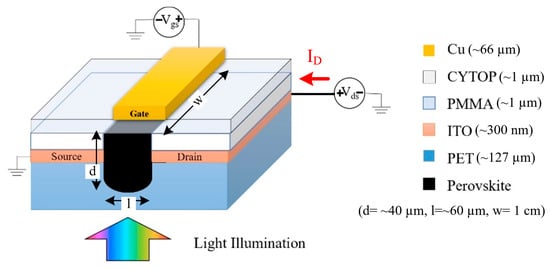
Figure 1.
Schematic of the fabricated MAPbI3 phototransistor.
3. Results and Discussion
The SEM image of the laser engraved channel is shown in Figure 2a. The channel width was measured to be ~60 µm. The crystallinity of the perovskite was then studied with the XRD method (Figure 2b). As reported in our previous work [34], it was a strong peak at 26.1° and a broad peak around 54° associated to the ITO coated PET substrate. Therefore, that part of the spectrum is not shown in Figure 2b. The two strong peaks at 2Θ of 13.95 degrees and 14.22 degrees were assigned to (002) and (110) planes of tetragonal CH3NH3PbI3 (space group I4/mcm) [31,32,35]. The XRD result also shows other crystalline orientations, which implies the formation of a polycrystalline structure in the channel.

Figure 2.
(a) The SEM image of the laser engraved microchannel (the image is taken at 44 degrees tilt angle), (b) the XRD spectra of the perovskite channel.
The transistor characteristics were measured in dark and under white light with the power density of 80 mW·cm−2. Since CYTOP surface hydrophobicity reduced at high electric fields [36] and may cause degradation of the perovskite layer, the output characteristics (drain current (ID) versus drain voltage (VDS)) were measured from 0 V to 20.0 V while varying gate voltage (VGS) from 10.0 V to 30.0 V by 10.0 V steps (Figure 3a,c). Additionally, the transfer characteristics (ID versus VGS) of the fabricated device were measured at VDS of 20 V under light and dark conditions and are presented in Figure 3b,d, respectively. No significant changes were observed in the device characteristics after it was bent and relaxed. However, since our earlier studies showed the piezoelectric effect of the perovskite [35], no attempt was made to test the device when it was bent. Further characterization will be conducted and reported later to study the photo-piezo effect in the perovskite transistors.
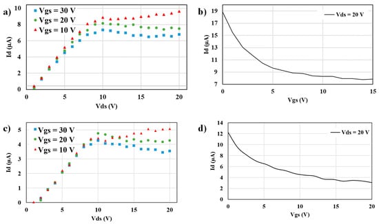
Figure 3.
(a,c) Output and (b,d) transfer characteristics of the fabricated flexible photo-transistor (a,b) under light and (c,d) in dark.
As the channel was well encapsulated by CYTOP, all measurements were performed in ambient conditions. To minimize the ion-migration and bias stress effect, the overall time duration of each scan was set to ~8 s with a pause of a few minutes after each set of measurements while the sample was kept in the dark. In order to ensure that the current change was not the result of degradation of perovskite with time, the output characteristic measurements (Figure 3a,c) were repeated in reverse order as well (starting at VGS of 30 V and decreasing down to 10 V) and the same trend was observed.
As shown in Figure 3a,c, the transistor reached the saturation region when the drain–source voltage was above 10.0 V. As the gate voltage increased, the saturated drain current decreased. The same trend was observed from the transfer characteristics both in dark and light conditions. The drain current dropped when the gate voltage increased at a drain voltage of 20.0 V which implies the depletion mode field-effect transistor (FET), not the enhancement. In fact, the non-zero current at VGS = 0 V in the transfer characteristics (Figure 3b,d) confirms the depletion mode in which the transistor is normally “on”. Although the device showed a poor current modulation from the gate voltage, as shown in Figure 3, under illumination, the currents in both output and transfer characteristics were larger than the dark currents at the equal bias voltages. In Figure 3b,d at VDS = 20 V when 0 V was applied to VGS, the dark current was ID = 12.1 µA. The current increased to 18.8 µA under illumination, showing a photocurrent of 6.7 µA (18.8 µA–12.1 µA). Considering the photoactive area of the transistor (w × l in Figure 1) and the intensity of the light (80 mW·cm−2), the photo-responsivity was estimated to be 14 mA·W−1, which is at least two orders of magnitude lower than the previously reported devices [17,37]. In this design, due to the high thickness of the channel (~40 µm) and the high optical absorption coefficient in MAPbI3 (between 104 and 105 cm−1) [38], light is not able to penetrate through the entire thickness of the semiconductor. Therefore, the top gate does not modulate the drain current effectively.
In addition to the thickness of the semiconductor, the polycrystalline structure of MAPbI3 and the ion-migration in the material are limiting factors. The crystallization of grains at low temperatures by the solution-based fabrication process generates a large number of defects. These defects and trap states provide low activation energy and make a channel for the intrinsic migration of I−, MA+, Pb2+, and, in some cases, H+ ions. These ions accumulate at the interfaces, screen the applied gate electric field, and they can reduce the mobile electrons concentration in the accumulation layer of FET [39]. Therefore ion migration plays an important role in carrier transport in lead halide perovskite [40]. The concentration of carriers changes mobility [41,42].
Figure 4 represents the transfer characteristics of the device in dark. As the saturation current is in direct relation with the mobility, decreasing the mobility lower the saturation current. The mobility of the fabricated device was calculated to be ~1.7 cm2·V−1·s−1 from the linear region of the transfer characteristic on using Equation (1).
where, C is the capacitor of CYTOP layer estimated from the thickness of the dielectric and its relative permittivity, l is the channel length (60 µm), and w is the channel width (1 cm). Although a mobility higher than 100 cm2·V−1·s−1 has been reported in the bulk of a single crystalline perovskite [8], the reported field-effect mobility in perovskite-based transistors are in the range of 1–9 cm2·V−1·s−1 [26]. The visible defects in Figure 2a and the polycrystalline structure of perovskite (Figure 2b) suggest having relatively high density of traps that has a direct effect on the mobility. Additionally, it is likely that the negative charged point defects drifted toward the CYTOP/perovskite interface (with a positive gate voltage) and screened the applied gate electric field. This effect and the depletion mode operation of the FET due to the thick layer of the perovskite resulted in a unipolar p-type transport characteristic, as shown in the transfer characteristics. Table 1 is a summary of fabricated MAPbI3-based phototransistors with some transistors showing ambipolar responses with the perovskite, acting as n-type and p-type semiconductors under negative and positive gate voltages, respectively.

Figure 4.
The transfer characteristics of the fabricated phototransistor in dark at different drain–source voltages.

Table 1.
Summary of fabricated MAPbI3-based phototransistors.
The presented results here are promising for the fabrication of low-cost perovskite-based photodetectors. However, a modification in the design is required to make shallower micro-channels to obtain a thinner perovskite. It is expected that the current modulation and photo-response would be improved with a lower thickness of perovskite.
4. Conclusions
In this work, we introduced a new fabrication method to make an MAPbI3 flexible phototransistor based on a lateral structure and top-gate contact configuration. Laser engraving was employed to make a microfluidic channel with the width of 60 µm on ITO coated PET substrate. The fabricated device operated in the triode and saturation regions in dark and under light illumination while showing p-type transport characteristics. This novel fabrication method provides a simple solution to make an MAPbI3 transistor with comparably high mobility on flexible hydrophobic substrates.
Author Contributions
A.T. is the principal investigator (PI) of the project at USF. F.K. designed, fabricated, and characterized the fabricated device. Both authors contributed to writing the paper. All authors have read and agreed to the published version of the manuscript.
Funding
This research received no external funding.
Conflicts of Interest
The authors declare no conflict of interest.
References
- Zhu:, H.; Shin, E.S.; Liu, A.; Ji, D.; Xu, Y.; Noh, Y.Y. Printable semiconductors for backplane TFTs of flexible OLED displays. Adv. Funct. Mater. 2020, 30, 1904588. [Google Scholar] [CrossRef]
- Haneef, H.F.; Zeidell, A.M.; Jurchescu, O.D. Charge carrier traps in organic semiconductors: A review on the underlying physics and impact on electronic devices. J. Mater. Chem. C 2020, 8, 759–787. [Google Scholar] [CrossRef]
- Petti, L.; Münzenrieder, N.; Vogt, C.; Faber, H.; Büthe, L.; Cantarella, G.; Bottacchi, F.; Anthopoulos, T.D.; Tröster, G. Metal oxide semiconductor thin-film transistors for flexible electronics. Appl. Phys. Rev. 2016, 3, 021303. [Google Scholar] [CrossRef]
- Ju, M.G.; Dai, J.; Ma, L.; Zeng, X.C. Perovskite chalcogenides with optimal bandgap and desired optical absorption for photovoltaic devices. Adv. Energy Mater. 2017, 7, 1700216. [Google Scholar] [CrossRef]
- Jiang, Y.; Juarez-Perez, E.J.; Ge, Q.; Wang, S.; Leyden, M.R.; Ono, L.K.; Raga, S.R.; Hu, J.; Qi, Y. Post-annealing of MAPbI 3 perovskite films with methylamine for efficient perovskite solar cells. Mater. Horizons 2016, 3, 548–555. [Google Scholar] [CrossRef]
- Djurišić, A.; Liu, F.; Tam, H.; Wong, M.; Ng, A.; Surya, C.; Chen, W.; He, Z. Perovskite solar cells—An overview of critical issues. Prog. Quant. Electron. 2017, 53, 1–37. [Google Scholar] [CrossRef]
- Schuster, O.; Wientjes, P.; Shrestha, S.; Levchuk, I.; Sytnyk, M.; Matt, G.J.; Osvet, A.; Batentschuk, M.; Heiss, W.; Brabec, C.J. Looking beyond the surface: The band gap of bulk methylammonium lead iodide. Nano Lett. 2020, 20, 3090–3097. [Google Scholar] [CrossRef]
- Dong, Q.; Fang, Y.; Shao, Y.; Mulligan, P.; Qiu, J.; Cao, L.; Huang, J. Electron-hole diffusion lengths >175 μm in solution-grown CH3NH3PbI3 single crystals. Science 2015, 347, 967–970. [Google Scholar] [CrossRef]
- Ava, T.T.; Al Mamun, A.; Marsillac, S.; Namkoong, G. A review: Thermal stability of methylammonium lead halide based perovskite solar cells. Appl. Sci. 2019, 9, 188. [Google Scholar] [CrossRef]
- Chin, X.Y.; Cortecchia, D.; Yin, J.; Bruno, A.; Soci, C. Lead iodide perovskite light-emitting field-effect transistor. Nat. Commun. 2015, 6, 7383. [Google Scholar] [CrossRef]
- Lin, Y.H.; Pattanasattayavong, P.; Anthopoulos, T.D. Metal-Halide Perovskite Transistors for Printed Electronics: Challenges and Opportunities. Adv. Mater. 2017, 29, 1702838. [Google Scholar] [CrossRef]
- Zhou, Z.; Guo, N.; Peng, Y.; Tang, L.; Zhang, J.; Cai, H.; Ni, J.; Sun, Y.; Li, J. The Effect of Annealing Pressure on Perovskite Films and Its Thin-Film Field-Effect Transistors’ Performance. Phys. Stat. Solid. A 2019, 216, 1900434. [Google Scholar] [CrossRef]
- Wang, Y.; Zhang, Y.; Lu, Y.; Xu, W.; Mu, H.; Chen, C.; Qiao, H.; Song, J.; Li, S.; Sun, B. Hybrid graphene–perovskite phototransistors with ultrahigh responsivity and gain. Adv. Opt. Mater. 2015, 3, 1389–1396. [Google Scholar] [CrossRef]
- Wang, J.; Liu, F.; Wang, G.; Wang, L.; Jiang, C. Novel organic-perovskite hybrid structure forward photo field effect transistor. Organ. Electron. 2016, 38, 158–163. [Google Scholar] [CrossRef]
- Mei, Y.; Zhang, C.; Vardeny, Z.; Jurchescu, O. Electrostatic gating of hybrid halide perovskite field-effect transistors: Balanced ambipolar transport at room-temperature. MRS Commun. 2015, 5, 297–301. [Google Scholar] [CrossRef]
- Lv, Q.; Wang, Z.; Dong, G.; Yan, Q. Anisotropic Carrier Transport in CH 3 NH 3 PbI 3 Single Crystal Field-Effect Transistor. IEEE Electr. Dev. Lett. 2018, 39, 1389–1392. [Google Scholar] [CrossRef]
- Li, F.; Ma, C.; Wang, H.; Hu, W.; Yu, W.; Sheikh, A.D.; Wu, T. Ambipolar solution-processed hybrid perovskite phototransistors. Nat. Commun. 2015, 6, 8238. [Google Scholar] [CrossRef]
- Li, D.; Cheng, H.C.; Wang, Y.; Zhao, Z.; Wang, G.; Wu, H.; He, Q.; Huang, Y.; Duan, X. The Effect of Thermal Annealing on Charge Transport in Organolead Halide Perovskite Microplate Field-Effect Transistors. Adv. Mater. 2017, 29, 1601959. [Google Scholar] [CrossRef]
- Kagan, C.; Mitzi, D.; Dimitrakopoulos, C. Organic-inorganic hybrid materials as semiconducting channels in thin-film field-effect transistors. Science 1999, 286, 945–947. [Google Scholar] [CrossRef]
- Ji, J.; Haque, F.; Hoang, N.T.T.; Mativenga, M. Ambipolar Transport in Methylammonium Lead Iodide Thin Film Transistors. Crystals 2019, 9, 539. [Google Scholar] [CrossRef]
- Huo, C.; Liu, X.; Song, X.; Wang, Z.; Zeng, H. Field-effect transistors based on van-der-waals-grown and dry-transferred all-inorganic perovskite ultrathin platelets. J. Phys. Chem. Lett. 2017, 8, 4785–4792. [Google Scholar] [CrossRef]
- He, B.; Li, W.; Wang, Q.; Liang, L.; Wang, H.; Xu, J.; Yang, S.; Jiang, Y.; Tang, Y.; Zou, B. Ultrasensitive all-solution-processed field-effect transistor based perovskite photodetectors with sol-gel SiO2 as the dielectric layer. J. Alloys Compd. 2017, 717, 150–155. [Google Scholar] [CrossRef]
- Cao, M.; Zhang, Y.; Yu, Y.; Jin, L.; Li, Y.; Chen, Z.; Che, Y.; Dai, H.; Zhang, G.; Yao, J. Enhanced perovskite phototransistor by multi-step slow annealing strategy. Opt. Mater. 2018, 84, 498–503. [Google Scholar] [CrossRef]
- Canicoba, N.D.; Zagni, N.; Liu, F.; Mccuistian, G.; Fernando, K.; Bellezza, H.; Traore, B.; Rogel, R.; Tsai, H.; Le Brizoual, L. Halide Perovskite High-k Field Effect Transistors with Dynamically Reconfigurable Ambipolarity. ACS Mater. Lett. 2019, 1, 633–640. [Google Scholar] [CrossRef]
- Li, F.; Wang, H.; Kufer, D.; Liang, L.; Yu, W.; Alarousu, E.; Ma, C.; Li, Y.; Liu, Z.; Liu, C. Ultrahigh Carrier Mobility Achieved in Photoresponsive Hybrid Perovskite Films via Coupling with Single-Walled Carbon Nanotubes. Adv. Mater. 2017, 29, 1602432. [Google Scholar] [CrossRef]
- Wang, G.; Li, D.; Cheng, H.-C.; Li, Y.; Chen, C.-Y.; Yin, A.; Zhao, Z.; Lin, Z.; Wu, H.; He, Q. Wafer-scale growth of large arrays of perovskite microplate crystals for functional electronics and optoelectronics. Sci. Adv. 2015, 1, e1500613. [Google Scholar] [CrossRef] [PubMed]
- Xie, C.; Liu, C.K.; Loi, H.L.; Yan, F. Perovskite-Based Phototransistors and Hybrid Photodetectors. Adv. Funct. Mater. 2019, 30, 1903907. [Google Scholar] [CrossRef]
- Park, N.-G. Perovskite solar cells: An emerging photovoltaic technology. Mater. Today 2015, 18, 65–72. [Google Scholar] [CrossRef]
- Kalaiselvi, C.; Muthukumarasamy, N.; Velauthapillai, D.; Kang, M.; Senthil, T. Importance of halide perovskites for next generation solar cells–a review. Mater. Lett. 2018, 219, 198–200. [Google Scholar] [CrossRef]
- Khorramshahi, F.; Ghazizadeh, N.; Kymissis, I.; Takshi, A. Laser engraving method to fabricate iodide and bromide-based perovskite photosensors. In Proceedings of Organic and Hybrid Sensors and Bioelectronics XIII; SPIE: Bellingham, WA, USA, 2020; p. 114750L. [Google Scholar]
- Khorramshahi, F.; Aljafari, B.; Kymissis, I.; Takshi, A. Laser assisted rapid fabrication of perovskite photodetector. In Proceedings of Organic and Hybrid Sensors and Bioelectronics XII; SPIE: Bellingham, WA, USA, 2019; p. 110960C. [Google Scholar]
- Khorramshahi, F.; Takshi, A. Novel fabrication of flexible perovskite photosensor using capillary motion. In Proceedings of Organic and Hybrid Sensors and Bioelectronics XI; SPIE: Bellingham, WA, USA, 2018; p. 107380R. [Google Scholar]
- Khorramshahi, F.; Takshi, A. Study of the stability of lead halide perovskite under two different fluoropolymer top coatings. MRS Adv. 2020, 5, 377–383. [Google Scholar] [CrossRef]
- Khorramshahi, F.; Okeke, O.E.; Takshi, A. Electrochemical photocurrent enhancement in a ZnO-perovskite heterojunction using piezoelectric effect. Electrochim. Acta 2018, 266, 110–117. [Google Scholar] [CrossRef]
- Khorramshahi, F.; Woughter, A.G.; Ram, M.K.; Kymissis, I.; Takshi, A. Apparent Piezo-Photocurrent Modulation in Methylammonium Lead Iodide Perovskite Photodetectors. Adv. Electron. Mater. 2019, 5, 1900518. [Google Scholar] [CrossRef]
- Chae, J.B.; Kwon, J.O.; Yang, J.S.; Kim, D.; Rhee, K.; Chung, S.K. Optimum thickness of hydrophobic layer for operating voltage reduction in EWOD systems. Sens. Actuat. A Phys. 2014, 215, 8–16. [Google Scholar] [CrossRef]
- Liu, J.; Xue, Y.; Wang, Z.; Xu, Z.-Q.; Zheng, C.; Weber, B.; Song, J.; Wang, Y.; Lu, Y.; Zhang, Y. Two-dimensional CH3NH3PbI3 perovskite: Synthesis and optoelectronic application. ACS Nano 2016, 10, 3536–3542. [Google Scholar] [CrossRef]
- Xing, G.; Mathews, N.; Sun, S.; Lim, S.S.; Lam, Y.M.; Grätzel, M.; Mhaisalkar, S.; Sum, T.C. Long-range balanced electron-and hole-transport lengths in organic-inorganic CH3NH3PbI3. Science 2013, 342, 344–347. [Google Scholar] [CrossRef]
- Senanayak, S.P.; Yang, B.; Thomas, T.H.; Giesbrecht, N.; Huang, W.; Gann, E.; Nair, B.; Goedel, K.; Guha, S.; Moya, X. Understanding charge transport in lead iodide perovskite thin-film field-effect transistors. Sci. Adv. 2017, 3, e1601935. [Google Scholar] [CrossRef]
- Yuan, Y.; Huang, J. Ion migration in organometal trihalide perovskite and its impact on photovoltaic efficiency and stability. Account Chem. Res. 2016, 49, 286–293. [Google Scholar] [CrossRef]
- Zhang, M.; Zhang, X.; Huang, L.-Y.; Lin, H.-Q.; Lu, G. Charge transport in hybrid halide perovskites. Phys. Rev. B 2017, 96, 195203. [Google Scholar] [CrossRef]
- Bi, C.; Shao, Y.; Yuan, Y.; Xiao, Z.; Wang, C.; Gao, Y.; Huang, J. Understanding the formation and evolution of interdiffusion grown organolead halide perovskite thin films by thermal annealing. J. Mater. Chem. A 2014, 2, 18508–18514. [Google Scholar] [CrossRef]
- Wu, Y.; Li, J.; Xu, J.; Du, Y.; Huang, L.; Ni, J.; Cai, H.; Zhang, J. Organic–inorganic hybrid CH 3 NH 3 PbI 3 perovskite materials as channels in thin-film field-effect transistors. RSC Adv. 2016, 6, 16243–16249. [Google Scholar] [CrossRef]
- Tong, S.; Wu, H.; Zhang, C.; Li, S.; Wang, C.; Shen, J.; Xiao, S.; He, J.; Yang, J.; Sun, J. Large-area and high-performance CH3NH3PbI3 perovskite photodetectors fabricated via doctor blading in ambient condition. Organ. Electron. 2017, 49, 347–354. [Google Scholar] [CrossRef]
- Yu, H.; Cheng, Y.; Shin, D.; Tsang, S.W.; So, F. Vertical Organic–Inorganic Hybrid Perovskite Schottky Junction Transistors. Adv. Electron. Mater. 2018, 4, 1800039. [Google Scholar] [CrossRef]
- Hong, Z.; Zhao, J.; Huang, K.; Cheng, B.; Xiao, Y.; Lei, S. Controllable switching properties in an individual CH 3 NH 3 PbI 3 micro/nanowire-based transistor for gate voltage and illumination dual-driving non-volatile memory. J. Mater. Chem. C 2019, 7, 4259–4266. [Google Scholar] [CrossRef]
- Hoang, N.T.T.; Haque, F.; Ji, J.; Mativenga, M. Fast-Switching Mixed A-Cation Organic-Inorganic Hybrid Perovskite TFTs. IEEE Electron. Device Lett. 2019, 40, 917–920. [Google Scholar] [CrossRef]
- Chen, P.-A.; Guo, J.; Nouri, M.; Tao, Q.; Li, Z.; Li, Q.; Du, L.; Chen, H.; Dong, Z.; Chang, L. Microfluidic Solution-Processed Organic and Perovskite Nanowires Fabricated for Field-Effect Transistors and Photodetectors. J. Mater. Chem. C 2020, 8, 2353–2362. [Google Scholar] [CrossRef]
Publisher’s Note: MDPI stays neutral with regard to jurisdictional claims in published maps and institutional affiliations. |
© 2020 by the authors. Licensee MDPI, Basel, Switzerland. This article is an open access article distributed under the terms and conditions of the Creative Commons Attribution (CC BY) license (http://creativecommons.org/licenses/by/4.0/).