Abstract
This paper presents a novel baseband architecture that supports high-speed wireless VR solutions using 60 GHz RF circuits. Based on the experimental observations by our previous 60 GHz transceiver circuits, the efficient baseband architecture is proposed to enhance the quality of transmission. To achieve a zero-latency transmission, we define an (106,920, 95,040) interleaved-BCH error-correction code (ECC), which removes iterative processing steps in the previous LDPC ECC standardized for the near-field wireless communication. Introducing the block-level interleaving, the proposed baseband processing successfully scatters the existing burst errors to the small-sized component codes, and recovers up to 1080 consecutive bit errors in a data frame of 106,920 bits. To support the high-speed wireless VR system, we also design the massive-parallel BCH encoder and decoder, which is tightly connected to the block-level interleaver and de-interleaver. Including the high-speed analog interfaces for the external devices, the proposed baseband architecture is designed in 65 nm CMOS, supporting a data rate of up to 12.8 Gbps. Experimental results show that the proposed wireless VR solution can transfer up to 4 K high-resolution video streams without using time-consuming compression and decompression, successfully achieving a transfer latency of 1 ms.
1. Introduction
Recently, multimedia contents have been changed to serve immersive experiences to users with evolutionary interfacing devices. Among the various types of emerging devices, virtual reality (VR) components, such as head-mounted display (HMD) devices, have been continuously developed to provide a seamless user experience with high-resolution video streams [1,2,3,4]. As such, a system usually requires a huge amount of data transmissions; however, the conventional VR HMD is in general inconvenient due to the connection cables between the media host and HMDs [5], limiting the impact of VR applications. Therefore, wireless VR becomes a promising solution to provide the next-level experience by transferring at least 4 K video streams through RF circuits.
If we directly adopt the high-speed near-field communication standards [6,7,8], however, it is inefficient to give the immersive user-level experience due to the long transmission latency caused by the iterative error recovery algorithms associated with complex interleaving schemes [9,10,11,12]. Supporting the transmission rate of over 6 Gbps, for example, the recent WiGig standard uses a number of baseband operations including the scrambler, the FFT-based processing, the high-speed analog-to-digital conversion, and the iterative low-density parity-check (LDPC) error-correction code (ECC), requiring the transmission delay of more than 5 ms [13]. In addition, the complicated baseband steps, in general, necessitate a large amount of energy, potentially increasing the size of the battery for mobile HMD devices. Considering the practical channel condition for wireless VR applications, therefore, it is necessary to utilize only the essential baseband steps for achieving the required transmission quality, accordingly reducing the baseband latency as well as the energy consumption.
Adding to our previous 60 GHz transceiver RF integrated circuits (RFICs) [14], in this work, we newly introduce a compact but effective baseband architecture for wireless VR applications. By observing the channel conditions of practical use cases, for the first time, we analyze erroneous patterns in wireless VR applications. To correct a massive number of consecutive errors caused by the misaligned beamforming from head-rotating motions, we design an advanced error-correction code (ECC) associated with the simple but efficient block-level interleaving scheme. As the proposed interleaver successfully scatters the burst errors into different short-length component codes (CCs), our baseband system can tolerate up to 1080 consecutive errors among 106,920 bits, which is sufficient to tolerate the practical misaligned problem. As a prototype design, integrating the proposed digital baseband architecture and the high-speed analog interfaces connecting the external devices, a fully-integrated baseband architecture for the wireless VR system is implemented in 65 nm CMOS technology. Adopting the massive-parallel structures for digital baseband processing, we can achieve a transfer rate of 12.8 Gbps while consuming only 525 mW including all the high-speed analog interfaces. As the proposed baseband processing uses non-iterative ECC with hard-decision inputs, we can also achieve the transfer latency of 1 ms, which is superior to other near-field wireless systems, leading to zero-latency wireless VR solutions.
The rest of this paper is organized as follows. Section 2 explains the overall architecture of our wireless VR system. Section 3 presents the proposed baseband processing using the block-level interleaving with short-length component ECC codes. The implementation results are shown and compared to the other related works in Section 4. The concluding remarks are finally made in Section 5.
2. Background of the Proposed Wireless VR System
2.1. System Specification
Figure 1 conceptually illustrates the proposed wireless VR system connecting the host system and a VR HMD via 60 GHz wireless technique. In addition to the previous 60 GHz RFIC [14], we newly develop in this work a compact baseband transceiver achieving the transmission latency of 1 ms, which is regarded as the zero-delay transmission of VR applications. Note that the proposed baseband system consists of three parts: two high-speed analog interface parts for performing as the de-serializer and the serializer, and the compact low-latency digital baseband unit. More precisely, for transmitting the high-quality video stream, the de-serializer shown in Figure 1 receives a high-speed serialized video stream from the host device and parallelizes the received data into the low-speed 16b-parallel stream, which can be managed by the following baseband architecture in transmitting (TX) mode. The baseband processing then generates the compact ECC and rearranges a number of codewords by utilizing the block-level interleaving scheme, constructing the 18b-parallel stream. The following analog-based serializer unit finally converts this low-speed 18b-parallel data stream into the high-speed serial data, which are delivered to a single lane of the previously-designed 60 GHz RFIC in TX mode.
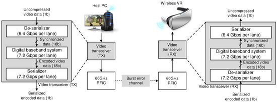
Figure 1.
Processing flow of the proposed wireless VR system.
By reversing the order of data processing, as shown in Figure 1, the receiving (RX) mode of the proposed baseband architecture can efficiently accept the transmitted data through the wireless channel. More precisely, similar to the operations in TX mode, the de-serializer firstly obtains the high-speed bit stream from a single lane of the 60 GHz RF module, and parallelizes the input data into 18 bits, lowering the operating frequency to be applied at the digital baseband architecture in RX mode. With the block-level de-interleaving followed by the high-throughput massive-parallel ECC decoder, the digital baseband processing successfully corrects the erroneous bits whose patterns are mainly occurred at the practical channel conditions. The recovered 16b-parallel data stream is then fed into the serializer to generate the error-free bit stream delivered to the display controller of HMD.
In this work, for providing the immersive experience, we target a data rate of over 12 Gbps from the host device, which can successfully transfer the 4 K/60 Hz full high-definition (FHD) videos [1,5]. To support such a high data-rate, we utilize two transmission lanes at the baseband architecture, realizing two identical sets of baseband processing units each of which achieves over 6 Gbps throughput in 65 nm CMOS technology. Note that the 60 GHz RF module supports both BPSK and QPSK modulations, and therefore the proposed wireless VR solution can support two transmission rates, i.e., 6.4 Gbps and 12.8 Gbps, allowing the trade-offs between the video quality and the power consumption.
2.2. Channel Condition of Wireless VR Environments
To define the required processing of the proposed baseband architecture, we first analyze the channel condition of near-field wireless communications based on our previous 60 GHz RFIC in [14]. Applying the beamforming scheme [15,16], as shown in Figure 2a, we can realize the error-free and zero-latency wireless communication when the beam is successfully aligned. In the case of misaligned beamforming, which normally occurs when the user rotates his or her head, some parts of the received packets directly disappear, resulting in a massive number of burst errors. As a result, the channel condition using the 60 GHz RF transceiver sometimes significantly deteriorates. Even with an average bit-error-rate (BER) of around , as depicted in Figure 2b, the length of burst errors is extremely long due to the high-speed transmission rate, requiring a dedicated digital baseband processing associated with the strong ECC hardware. Based on this observation, we develop a compact baseband system supporting the transmission speed of 12.8 Gbps, recovering up to 1080 consecutive bit errors in the data frame of 106,920 bits.
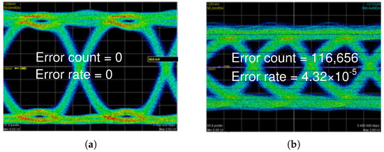
Figure 2.
Error pattern observed by the previous 60 GHz RF circuit. (a) Error count = 0, Error rate = 0; (b) Error count = 116,656, Error rate = 4.32 × .
3. Proposed Low-Latency Compact Baseband System for Wireless VR
3.1. Baseband Processing with Block-Level Interleaved-BCH Codes
Based on the channel observation, it is clear that the wireless VR system over 60 GHz RFIC should recover a number of burst errors. For some specifications targeting the high-speed near-field wireless communications, several candidates can support such a channel condition with different types of codes including low-density parity-check (LDPC) codes targeting the data rate of more than 6 Gbps [9,10,11,12,17]. However, the previous standards are normally defined to support various applications and thus they include several complicated processing steps to ensure the data integrity for different transmitting scenarios. If the recent WiGig standard were applied [6,8], for example, the received data stream would be recovered by passing through a number of blocks including synchronization unit, channel estimator, de-mapper, de-interleaver, and iterative LDPC decoder [18,19]. Therefore, the previous baseband system basically suffers from the long processing latency. In addition, the LDPC code uses the soft-decision inputs associated with a high-speed ADC architecture in general, consuming a huge amount of energy [20,21]. Due to the time- and energy-consuming requirements on the baseband processing, the previous specifications targeting the near-field wireless communication are no longer effective for the proposed wireless VR system. There are also other types of ECCs used for the different applications rather than the near-field communications. for example, ECCs for cellular devices such as turbo codes [22] and polar codes [23] could be attractive candidates if we consider their stable error-correcting powers. Similar to the WiGig case, however, those ECCs cannot be used for the proposed system due to the low code-rate and the long latency. Some high-rate codes for memory applications can be also considered, but the storages normally necessitate long-length codewords, thereby increasing the energy consumption caused by the large-sized internal buffers and the multiple decoding levels for lowering the error bounds [24,25,26].
Considering the tight requirement on the latency, which is the most important player for utilizing the wireless VR system, we choose the BCH-based ECC solution correcting the burst errors of up to 1080 bits in a data frame of 106,920 bits as the previous LDPC code generally takes a long time to correct the existing errors by adopting the iterative decoding steps [27]. To reduce the complexity of baseband processing, we newly introduce a (106,920, 95,040) block-level interleaved BCH code, which consists of 60 (1782, 1584, 18) component BCH codes, as depicted in Figure 3. Even a CC is relatively weak, correcting only up to 18 bits among 1782b-length data, i.e., a fully-erroneous block is recovered by a CC, the proposed coding scheme is effective for recovering the long length of burst errors by presenting the block-level interleaving scheme. As shown in Figure 3, the proposed code is divided into 5940 blocks of 18 bits, i.e., 5280 data blocks (D) from the input video stream and 660 parity blocks (P) for the parity information. Note that each CC consists of 99 blocks: 88 data blocks and 11 parity blocks. More precisely, to construct a CC, we collect 88 D blocks in order, i.e., D, D, …, D, and append 11 P blocks, as depicted in Figure 3. After constructing all CCs by utilizing the parallel BCH encoder, in the TX mode of the proposed baseband architecture, we start a block-level interleaving process, which shuffles the blocks to make the whole data frame tolerable to the burst errors.
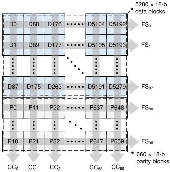
Figure 3.
Construction of the proposed interleaved BCH codes.
For the given data frame, as depicted in Figure 3, the block-level interleaving basically rearranges the order of transmission by generating 99 frame segments (FSs). In contrast to the blocks in each CC being arranged in vertical order as in Figure 3, a FS is simply constructed by selecting the 60 blocks in the horizontal direction, taking a block per CC. Compared to the other wireless standards requiring complicated interleaving steps [6,8], the block-level interleaving in this work is quite simple, remarkably reducing the hardware complexity of the wireless VR baseband system, which is discussed in the following subsection. After the block-level interleaving step, we finally transmit the data frame from FS to FS, guaranteeing that consecutive transmitted blocks are always from different CCs. Figure 4 conceptually illustrates how the proposed baseband architecture in TX mode produces the transmitted data. For supporting a seamless data transaction, note that we utilize the double buffering scheme realized by adopting two frame-sized buffers, which is denoted as FB0 and FB1. After the de-serializer generates the 16-parallel data stream, which is firstly stored to the input FIFO (IFIFO), the proposed baseband system simply generates the encoded CCs in order by reading 18 bits from IFIFO at a time, as illustrated in Figure 4. Note that we utilize the 18-parallel BCH encoder to calculate 11 parity blocks whenever reading out 88 data blocks from IFIFO. Similar to the conventional systematic BCH encoder architectures in [28,29], during the parallel encoding, the encoded user data blocks are directly moved to the following processing unit, i.e., the block-level interleaver, which immediately rearranges the input blocks to construct FSs in a round robin manner, as depicted in Figure 4. When the parallel encoder completely generates all the CCs in a data frame, as a result, all the FSs are also constructed and stored in a frame buffer. Then, the FSs are serially moved to the output FIFO (OFIFO), which is accessed by the serializer generating the high-speed bit stream for the 60 GHz RFIC. By utilizing the double buffering scheme, at the same time, the encoder starts to handle the next data frame, supporting a seamless data transaction, as illustrated in Figure 4.
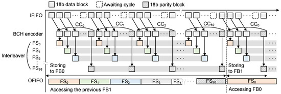
Figure 4.
Proposed interleaving and buffering scheme for seamless data transaction.
For the case of RX mode, the process of baseband processing is performed in a reverse order compared to that of TX processing, as depicted in Figure 5. More precisely, as illustrated in Figure 1, the 60 GHz RFIC provides a high-speed bit stream by demodulating the received signals, and the analog de-serializer in the proposed baseband system parallelizes it into 18-parallel data stream to serially deliver the received FSs to IFIFO at the digital baseband system in RX mode. Starting from the first data block at the first FS, the block-level de-interleaver directly scatters the received 18b blocks by changing the storing address of the frame buffer. In other words, as shown in Figure 5, the de-interleaver rearranges the received blocks in a round robin manner for reconstructing the received CCs. After transmitting a whole data frame, as a result, the frame buffer stores all CCs in order. The 18-parallel BCH decoder is then activated to correct the erroneous bits by sequentially accessing the CCs. Note that we only transfer the recovered data blocks from the parallel BCH decoder to OFIFO that can accept 18b data at a time. As illustrated in Figure 1, the analog serializer finally gets the 16-parallel data stream from OFIFO to make the valid bit stream to media devices, which has the same data-rate as the original input stream shown in Figure 1. Similar to the baseband processing in TX mode, the RX processing also utilizes the double buffering scheme, which means that the next data frame is transferred by using the empty frame buffer during the CC decoding operation, as depicted in Figure 5.
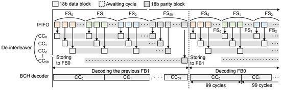
Figure 5.
Proposed de-interleaving and buffering scheme for seamless error correction.
Combined with the simple component BCH codes as well as the block-level interleaving scheme, the proposed digital baseband processing effectively overcomes the burst-error channels. Figure 6 illustrates how the proposed baseband system corrects a number of burst errors. Basically, we process the data blocks in CC-level orders and transfer them in FS-level orders. As two different ways manage the data blocks by handling the opposite directions to each other, as illustrated in Figure 3, the burst errors that exist in a number of blocks during the wireless transmission are naturally scattered to the different CCs at the baseband processing. If the channel suffers from the misalignment of beams, all the transmitted blocks contain errors for a while, which normally belong to the same FS depicted in Figure 6. By rearranging the received FSs with the block-level de-interleaver, however, those erroneous blocks are then placed into different CCs. As each CC can correct up to 18b errors, i.e., a single block, the proposed ECC solution can tolerate up to 60 consecutive error blocks by scattering all the error blocks to the different CC. As a result, the proposed (106,920, 95,040) block-level interleaved-BCH ECC can recover the burst errors of up to 1080 bits during transmitting a data frame of 106,920 bits. Without applying the block-level interleaving scheme, one can use a long BCH code for correcting total 1080 error bits in a user data of 95,040 bits; however, such a long BCH code requires an impractical amount of hardware complexity due to the increased dimension of finite field [30,31]. It is also possible to apply the RS code as a component code for providing the symbol-level correction [32,33]; however, the RS code only focuses on the burst-error channel condition. Even though the practical channel condition of the wireless VR system contains lots of burst errors, based on our observation, there still exist a few random errors. Therefore, the RS-based concatenation scheme is naturally inefficient compared to the proposed BCH-based ECC solution. As a result, the proposed baseband processing is attractive to the wireless VR systems in terms of the error-correcting capability as well as the computing complexity.
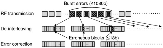
Figure 6.
The example of the burst error correcting with proposed interleaving scheme.
3.2. Hardware Architecture for Baseband Processing
To support the proposed baseband processing associated with the block-level interleaved-BCH ECC, we introduce in this work the dedicated hardware architecture that minimizes the hardware overheads while proving the high-throughput and low-latency data transmission. Figure 7 illustrates the block diagram of the proposed baseband architecture that can support both TX and RX modes. Note that we utilize the flexible FIFO architectures that can change the bandwidth of interfaces. More precisely, the IFIFO can support 16b and 18b input interfaces, which are used for TX and RX modes, respectively. Similarly, the OFIFO provides two options at the output interface, as depicted in Figure 7. By utilizing the flexible interfaces, it is possible to minimize the complexity overheads to support the different transmitting rates between the serialized video stream and the RF data, which are caused by appending the ECC parity information. Then, the 18-parallel BCH encoder in Figure 7 accesses IFIFO to get one 18b data block at a time. In the parallel encoder, whose internal processing architecture is detailed in Figure 8a [28,29], there is a path to directly transfer the issued data block to the interleaver so that the proposed digital baseband processing continuously constructs the frame segments. The interleaver generates the proper address to shuffle the data blocks, as depicted in Figure 6, and the following unified buffer manager transfers the encoded data blocks to the current frame buffer. After encoding all the CCs, i.e., generating a data frame to be transmitted, the OFIFO accesses the FBx through the unified buffer manager to take 18 bits at a time, which is transferred to the analog serializer producing the bit-stream for a transmission lane of 60 GHz RF circuits.
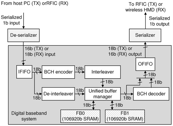
Figure 7.
Block diagram of the proposed digital baseband system.
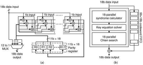
Figure 8.
Block diagram of the proposed one-lane BCH encoder (a) and decoder (b) architecture.
Note that the proposed baseband architecture in Figure 7 can be also used for supporting the RX mode. In contrast to the digital baseband system in TX mode receiving 16b-parallel data stream from the de-serializer handling the host multimedia source, the de-serializer now manages the input bit-stream from the RFIC associated with the higher transmission rate, generating the parallel data stream of 18 bits. By changing the interface mode, therefore, the IFIFO now accepts 18 bits at a time, and the following de-interleaver directly accesses the received data block of 18 bits to reconstruct the received CCs by scattering the writing address of the current frame buffer controlled by the unified buffer manager. The 18-parallel BCH decoder is utilized to decode a data block at every cycle. More precisely, as described in Figure 8b, the well-known three-stage pipelined decoder architecture associated with the codeword FIFO is introduced where each stage is fully optimized by adopting the previous techniques including the common subexpression (CSE)-elimination on syndrome calculation (SC) and Chien search (CS) units [34] and the low-complexity folded architecture on key equation solver (KES) unit [35]. As depicted in Figure 7, the decoded block is moved to the OFIFO, which is accessed by the serializer with the 16b output interface, providing the original media information to the wireless HMD.
To provide the data rate of more than 12 Gbps, which is sufficient to transfer the uncompressed FHD video stream, we utilize two identical baseband systems in Figure 7, each of which is connected to the orthogonal transmission lane of QPSK modulation. By removing all the complicated iterative processing in the previous specifications targeting the near-field wireless communication [6,7,8], the proposed baseband processing still recovers the erroneous channel conditions with the simple hardware configurations, acceptable for wireless VR systems whose HMD architecture is normally energy-limited.
4. Implementation Results
Based on the proposed compact digital baseband architecture for wireless VR systems, we integrated all the baseband processing units including the analog serializer and de-serializer as a prototype design in 65 nm CMOS technology. The die-photo of the prototype baseband system is depicted in Figure 9 where there are four frame buffers, as we utilized two identical baseband systems for supporting both BPSK and QPSK modulations at the 60 GHz RF circuits. To show the impact of the proposed interleaved-BCH ECC solution, we also realized the baseline (106,940, 95,040, 700) BCH codec. Note that the baseline ECC covers a whole data frame with the single code while having the same code rate as the proposed work. Table 1 compares the implementation results of two ECC codec units. By reducing the order of GF dimension, the proposed interleaved-BCH ECC drastically reduces the hardware complexity of both the encoder and decoder architectures. Note that the baseline BCH encoder and decoder necessitate more than 13 M gates, which are impractical to be used for the wireless VR solution. On the other hand, the proposed codec requires only 1.2 M gates, reducing the hardware costs by more than 91%.
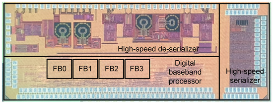
Figure 9.
The die-photo of the prototype baseband processor.

Table 1.
Hardware complexity comparison of BCH codec blocks.
To provide the quantitative comparisons, we summarize the error-correcting performances and the implementation results for different ECC decoding architectures, as depicted in Figure 10 and Table 2, respectively. Compared to the proposed interleaved-BCH code, it is noticeable that the low-rate ECCs for the existing wireless communications, i.e., the 0.5-rate polar code for 5G systems [23] and the 0.5-rate LDPC code for WiGig standards [11,12], provide superior correcting powers, as depicted in Figure 10. However, the baseband systems based on these soft-decision ECCs normally include complicated processing steps associated with high-resolution ADCs, drastically increasing the transmission latency and the energy consumption, as shown in Table 2. Considering the observed channel condition for the wireless VR scenario, as shown in Figure 2, the proposed interleaved-BCH still achieves an attractive UBER of less than , which can be considered as the error-free communication. As reported in [24,25,26], the high-rate ECCs for the storage applications may offer alternative options by achieving a similar error-correcting performances compared to the proposed work. However, in general, the high-rate codes for storages usually adopt the long codewords associated with the iterative decoding operations and multi-level coding schemes in order to lower the error bounds. Therefore, as shown in Table 2, the decoder architectures for storage solutions normally consume a huge amount of energy, which cannot be used for lightweight HMD devices. Allowing the compact and non-iterative ECC architecture, the proposed work definitely provides cost-effective results in terms of silicon area, processing throughput, and even power consumption. More precisely, our architecture consumes only 5.53 pJ for processing a single bit, which is five times less than the previous state-of-the-art ECC solution for near-field wireless system [11].
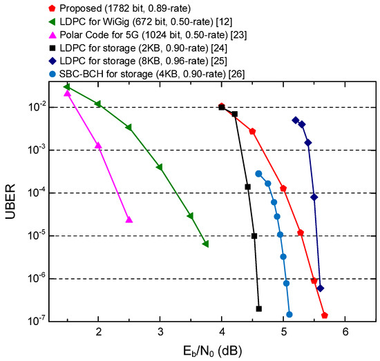
Figure 10.
Error-correcting capabilities of different ECC solutions.
Table 2.
Comparison of ECC solutions for near-field wireless communications.
Figure 11 shows the FPGA-based testing platform connected through the high-speed test I/O pins and also depicts major features of the prototype design. The testing platform successfully verified the high-throughput data transmission of uncompressed HD video streams with low latency. The initial synchronization process, i.e., the analog interfaces, as well as the RFIC operations take 0.97 ms, while the compact non-iterative baseband operations take 0.03 ms by using 6040 and 6058 cycles for TX and RX operations, respectively. As a result, the proposed testing platform achieves the transfer latency of only 1 ms, which can be regarded as a zero-delay transmission for VR applications. By not adopting the complex baseband processing, the proposed prototype consumes only 525 mW for handling the uncompressed HD video streams over HDMI protocols. Therefore, the proposed digital baseband architecture is definitely suitable for wireless VR applications, offering error-free, energy-efficient, and even ultra-low-latency solutions.
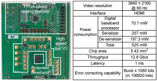
Figure 11.
A FPGA-based testing platform with high-speed interface I/Os.
5. Conclusions
In this paper, we present a cost-effective digital baseband architecture for wireless VR applications. Unlike the previous architectures that adopt the soft-decision and iterative ECCs associated with the complex interleaving scheme, to overcome the practical burst-aware channel condition, the proposed architecture uses only simple hard-decision BCH codes as the component ECCs and introduces the block-level interleaving architecture that minimizes the hardware costs. The optimized parallel encoder and decoder architectures of the proposed interleaved-BCH ECC allow the energy-efficient baseband processing, reducing the overall energy consumption of wireless VR systems significantly. The prototype baseband system utilizes two identical baseband processing lanes for supporting the QPSK modulation with the existing 60 GHz RF circuits, achieving a data rate of more than 12 Gbps, which is sufficient to transfer the uncompressed FHD video streams.
Author Contributions
Conceptualization, S.H. and Y.L.; methodology, S.H. and S.M.; software, S.H. and S.M.; validation, S.H., I.-Y.O. and Y.L.; formal analysis, S.H.; investigation, S.H. and D.K.; resources, S.H., I.-Y.O. and Y.L.; data curation, Y.L.; writing–original draft preparation, S.H. and Y.L.; writing–review and editing, D.K. and Y.L.; visualization, S.H.; supervision, Y.L.; project administration, Y.L.; funding acquisition, Y.L.
Funding
This research was supported by the National Research Foundation (NRF) grant funded by the Korea government (MSIT) (2018R1A4A1025679); by the Ministry of Science and ICT, Korea, under the ITRC support program (IITP-2019-2016-0-00309); by the Sports Promotion Fund of Seoul Olympic Sports Promotion Foundation from Ministry of Culture, Sports and Tourism; and by the IC Design Education Center (IDEC).
Conflicts of Interest
The author declares no conflict of interest.
References
- Pierce, J.S.; Pausch, R.; Sturgill, C.B.; Christiansen, K.D. Designing a successful HMD-based experience. Presence 1999, 8, 469–473. [Google Scholar] [CrossRef] [PubMed]
- Zheng, F.; Whitted, T.; Lastra, A.; Lincoln, P.; State, A.; Maimone, A.; Fuchs, H. Minimizing latency for augmented reality displays: Frames considered harmful. In Proceedings of the 2014 IEEE International Symposium on Mixed and Augmented Reality (ISMAR), Munich, Germany, 10–12 September 2014; pp. 195–200. [Google Scholar]
- Lincoln, P.; Blate, A.; Singh, M.; Whitted, T.; State, A.; Lastra, A.; Fuchs, H. From motion to photons in 80 microseconds: Towards minimal latency for virtual and augmented reality. IEEE Trans. Vis. Comput. Graph. 2016, 22, 1367–1376. [Google Scholar] [CrossRef] [PubMed]
- Choi, S.W.; Lee, S.; Seo, M.W.; Kang, S.J. Time Sequential Motion-to-Photon Latency Measurement System for Virtual Reality Head-Mounted Displays. Electronics 2018, 7, 171. [Google Scholar] [CrossRef]
- Hosseini, M.; Swaminathan, V. Adaptive 360 VR video streaming: Divide and conquer. In Proceedings of the 2016 IEEE International Symposium on Multimedia (ISM), San Jose, CA, USA, 11–13 December 2016; pp. 107–110. [Google Scholar]
- Nitsche, T.; Cordeiro, C.; B Flores, A.; Knightly, E.W.; Perahia, E.; Widmer, J. IEEE 802.11 ad: Directional 60 GHz communication for multi-Gigabit-per-second Wi-Fi. IEEE Commun. Mag. 2014, 52, 132–141. [Google Scholar] [CrossRef]
- Wireless HD. Available online: http://www.wirelesshd.org (accessed on 24 May 2019).
- Ghasempour, Y.; da Silva, C.R.; Cordeiro, C.; Knightly, E.W. IEEE 802.11 ay: Next-generation 60 GHz communication for 100 Gb/s Wi-Fi. IEEE Commun. Mag. 2017, 55, 186–192. [Google Scholar] [CrossRef]
- Balatsoukas-Stimming, A.; Preyss, N.; Cevrero, A.; Burg, A.; Roth, C. A parallelized layered QC-LDPC decoder for IEEE 802.11 ad. In Proceedings of the 2013 IEEE 11th International New Circuits and Systems Conference (NEWCAS), Paris, France, 16–19 June 2013; pp. 1–4. [Google Scholar]
- Li, M.; Naessens, F.; Debacker, P.; Raghavan, P.; Desset, C.; Li, M.; Dejonghe, A.; Van der Perre, L. An area and energy efficient half-row-paralleled layer LDPC decoder for the 802.11 AD standard. In Proceedings of the SiPS 2013, Taipei City, Taiwan, 16–18 October 2013; pp. 112–117. [Google Scholar]
- Li, M.; Lee, Y.; Huang, Y.; Van der Perre, L. Area and energy efficient 802.11 ad LDPC decoding processor. Electron. Lett. 2015, 51, 339–341. [Google Scholar] [CrossRef]
- Li, M.; Weijers, J.W.; Derudder, V.; Vos, I.; Rykunov, M.; Dupont, S.; Debacker, P.; Dewilde, A.; Huang, Y.; Van der Perre, L.; et al. An energy efficient 18Gbps LDPC decoding processor for 802.11 ad in 28 nm CMOS. In Proceedings of the 2015 IEEE Asian Solid-State Circuits Conference (A-SSCC), Xiamen, China, 9–11 November 2015; pp. 1–5. [Google Scholar]
- The Complementary Roles of 802.11ac and 802.11ad with a Wireless Docking Station in an Office Environment. Available online: https://www.qualcomm.com/media/documents/files/signals-research-group-whitepaper-the-complementary-roles-of-802-11ac-and-802-11ad-with-a-wireless-docking-station-in-an-office-environment.pdf (accessed on 24 May 2019).
- Wisejet Wireless VR. Available online: http://wise-jet.com/products/wireless-vr-solution (accessed on 24 May 2019).
- Van Veen, B.D.; Buckley, K.M. Beamforming: A versatile approach to spatial filtering. IEEE ASSP Mag. 1988, 5, 4–24. [Google Scholar] [CrossRef]
- Hefnawi, M. Hybrid Beamforming for Millimeter-Wave Heterogeneous Networks. Electronics 2019, 8, 133. [Google Scholar] [CrossRef]
- Park, Y.S.; Blaauw, D.; Sylvester, D.; Zhang, Z. Low-power high-throughput LDPC decoder using non-refresh embedded DRAM. IEEE J. Solid-State Circuits 2014, 49, 783–794. [Google Scholar] [CrossRef]
- Diamantopoulos, D.; Galiatsatos, P.; Karachalios, A.; Lentaris, G.; Reisis, D.; Soudris, D. Configurable baseband digital transceiver for Gbps wireless 60 GHz communications. In Proceedings of the 2011 18th IEEE International Conference on Electronics, Circuits, and Systems (ICECS), Beirut, Lebanon, 11–14 December 2011; pp. 192–195. [Google Scholar]
- Keusgen, W.; Kortke, A.; Peter, M.; Weiler, R. A highly flexible digital radio testbed and 60 GHz application examples. In Proceedings of the 2013 European Microwave Conference, Nuremberg, Germany, 6–10 October 2013; pp. 740–743. [Google Scholar]
- Moon, S.; Kim, I.S.; Kam, D.; Jee, D.W.; Choi, J.; Lee, Y. Massive MIMO Systems With Low-Resolution ADCs: Baseband Energy Consumption vs. Symbol Detection Performance. IEEE Access 2019, 7, 6650–6660. [Google Scholar] [CrossRef]
- Wang, D.; Zhu, X.; Guo, X.; Luan, J.; Zhou, L.; Wu, D.; Liu, H.; Wu, J.; Liu, X. A 2.6 GS/s 8-Bit Time-Interleaved SAR ADC in 55 nm CMOS Technology. Electronics 2019, 8, 305. [Google Scholar] [CrossRef]
- Lee, Y.; Li, M.; Van der Perre, L. Memory-Reduced Turbo Decoding Architecture Using NII Metric Compression. IEEE Trans. Circuits Syst. II Express Briefs 2015, 63, 211–215. [Google Scholar] [CrossRef]
- 3rd Generation Partnership Project (3GPP). Multiplexing and Channel Coding. 3GPP 38.212 V.15.3.0. 2018. Available online: https://www.etsi.org/deliver/etsi_ts/138200_138299/138212/15.03.00_60/ts_138212v150300p.pdf (accessed on 24 May 2019).
- Ho, K.; Chen, C.; Chang, H. A 520k (18900, 17010) Array Dispersion LDPC Decoder Architectures for NAND Flash Memory. IEEE Trans. Very Large Scale Integr. (VLSI) Syst. 2016, 24, 1293–1304. [Google Scholar] [CrossRef]
- Kim, J.; Sung, W. Rate-0.96 LDPC decoding VLSI for soft-decision error correction of NAND flash memory. IEEE Trans. Very Large Scale Integr. (VLSI) Syst. 2013, 22, 1004–1015. [Google Scholar]
- Hwang, S.; Moon, S.; Jung, J.; Kim, D.; Park, I.; Ha, J.; Lee, Y. Energy-Efficient Symmetric BC-BCH Decoder Architecture for Mobile Storages. IEEE Trans. Circuits Syst. Regul. Pap. 2019, 1–14. [Google Scholar] [CrossRef]
- Ul Hassan, N.; Lentmaier, M.; Fettweis, G.P. Comparison of LDPC block and LDPC convolutional codes based on their decoding latency. In Proceedings of the 2012 7th International Symposium on Turbo Codes and Iterative Information Processing (ISTC), Gothenburg, Sweden, 27–31 August 2012; pp. 225–229. [Google Scholar]
- Lee, Y.; Yoo, H.; Yoo, I.; Park, I.C. 6.4 Gb/s multi-threaded BCH encoder and decoder for multi-channel SSD controllers. In Proceedings of the 2012 IEEE International Solid-State Circuits Conference, San Francisco, CA, USA, 19–23 February 2012; pp. 426–428. [Google Scholar]
- Yoo, H.; Lee, Y.; Park, I.C. 7.3 Gb/s universal BCH encoder and decoder for SSD controllers. In Proceedings of the 2014 19th Asia and South Pacific Design Automation Conference (ASP-DAC), Singapore, 20–23 January 2014; pp. 37–38. [Google Scholar]
- Poolakkaparambil, M.; Mathew, J.; Jabir, A. Multiple bit error tolerant Galois field architectures over GF (2m). Electronics 2012, 1, 3–22. [Google Scholar] [CrossRef]
- Park, B.; Park, J.; Lee, Y. Area-Optimized Fully-Flexible BCH Decoder for Multiple GF Dimensions. IEEE Access 2018, 6, 14498–14509. [Google Scholar] [CrossRef]
- Chen, J.; Owsley, P. A burst-error-correcting algorithm for Reed-Solomon codes. IEEE Trans. Inf. Theory 1992, 38, 1807–1812. [Google Scholar] [CrossRef]
- Lin, S.; Costello, D.J. Error Control Coding: Fundamentals and Applications, 2nd ed.; Prentice-Hall: Englewood Cliffs, NJ, USA, 2004. [Google Scholar]
- Lee, Y.; Yoo, H.; Park, I.C. Low-complexity parallel Chien search structure using two-dimensional optimization. IEEE Trans. Circuits Syst. II Express Briefs 2011, 58, 522–526. [Google Scholar] [CrossRef]
- Park, B.; An, S.; Park, J.; Lee, Y. Novel folded-KES architecture for high-speed and area-efficient BCH decoders. IEEE Trans. Circuits Syst. II Express Briefs 2017, 64, 535–539. [Google Scholar] [CrossRef]
- Lee, Y.; Jung, J.; Park, I.C. Energy-scalable 4KB LDPC decoding architecture for NAND-flash-based storage systems. IEICE Trans. Electron. 2016, 99, 293–301. [Google Scholar] [CrossRef]
© 2019 by the authors. Licensee MDPI, Basel, Switzerland. This article is an open access article distributed under the terms and conditions of the Creative Commons Attribution (CC BY) license (http://creativecommons.org/licenses/by/4.0/).