Article

A High-Accuracy Ultra-Low-Power Offset-Cancelation On-Off Bandgap Reference for Implantable Medical Electronics

1
School of Microelectronics, Xi’an Jiaotong University, Xi’an 710049, China
2
School of Information and Engineering, Jimei University, Fujian 361021, China
3
Department of Chemical and Materials Engineering, National University of Kaohsiung, No. 700, Kaohsiung University Rd., Nan-Tzu District, Kaohsiung 811, Taiwan
*
Authors to whom correspondence should be addressed.
Electronics 2019, 8(7), 814; https://doi.org/10.3390/electronics8070814
Submission received: 11 June 2019 / Revised: 18 July 2019 / Accepted: 19 July 2019 / Published: 21 July 2019
(This article belongs to the Section Microelectronics)

Abstract

:
An ultra-low-power and high-accuracy on-off bandgap reference (BGR) is demonstrated in this paper for implantable medical electronics. The proposed BGR shows an average current consumption of 78 nA under 2.8 V supply and an output voltage of 1.17 V with an untrimmed accuracy of 0.69%. The on-off bandgap combined with sample-and-hold switched-RC filter is developed to reduce power consumption and noise. The on-off mechanism allows a relatively higher current in the sample phase to alleviate the process variation of bipolar transistors. To compensate the error caused by operational amplifier offset, the correlated double sampling strategy is adopted in the BGR. The proposed BGR is implemented in 0.35 μm standard CMOS process and occupies a total area of 0.063 mm2. Measurement results show that the circuit works properly in the supply voltage range of 1.8–3.2 V and achieves a line regulation of 0.59 mV/V. When the temperature varies from −20 to 80 °C, an average temperature coefficient of 19.6 ppm/°C is achieved.

1. Introduction

Along with the continuous development of modern society and growing demand for high-quality life, implantable medical electronics are increasingly adopted in healthcare medical devices such as cardiac pacemakers [1,2,3]. These devices are usually battery powered and need to have ultra-low power consumption of a few microwatts or less [4,5,6,7,8]. Since they would probably be placed where they are not easily removed or recharged, they have to continue working for a relatively long time. A number of important analog circuits for high-precision signal processing, such as voltage regulators, analog to digital converters (ADCs) and digital to analog converters (DACs), are used in almost every biomedical system. All of them demand an accurate bandgap reference (BGR) [9]. In these devices, BGRs provide the voltage references for other important functional blocks and are supposed to be working all the time. Thus, the required average current dissipation of BGR is in the range of several tens of nano-ampere [10,11,12].
To meet the requirement for low power, subthreshold voltage references without bipolar transistors have been developed and used widely [10,11,12]. However, these VTH-based references often suffer from degraded performance in accuracy since the threshold voltage (VTH) of MOSFET changes too much (about 50–100mV) with process variation. Trimming is usually employed to solve this issue. However, the temperature coefficient would be worse after trimming [12]. A conventional bipolar junction transistor (BJT)-based BGR can provide a fairly precise reference voltage, but it requests larger power consumption. When we try to budget a lower current consumption for BJT-based BGR, resistors with very large values are needed, and the VBE of BJT also varies dramatically. VBE variation introduces large fluctuations to the output reference voltage. Even for relatively larger budgeted power consumption, trimming is still generally required for BJT-based BGR because of the existence of mismatch and offset [13].
In this paper, an ultra-low power, high accuracy BGR is presented. The proposed reference provides a 1.17 V output under 2.8 V supply voltage with 78 nA average current consumption. An on-off bandgap combined with sample-and-hold switched-RC filter is developed to reduce power consumption and noise. The on-off mechanism increases the working current of the BJT-based BGR during the sample period, which decreases VBE spread. A correlated double sampling (CDS) strategy is adopted to cancel the offset of the operational amplifier (Opamp), which is fulfilled by a sampling capacitor block combined with chopper mechanism. The conflict between low power and high accuracy is preliminarily settled. The theoretical foundation and specific circuit design are described in Section 2. Section 3 presents the simulation and measurement results as well as a performance comparison. Finally, conclusions are summarized in Section 4.

2. Proposed Bandgap Reference

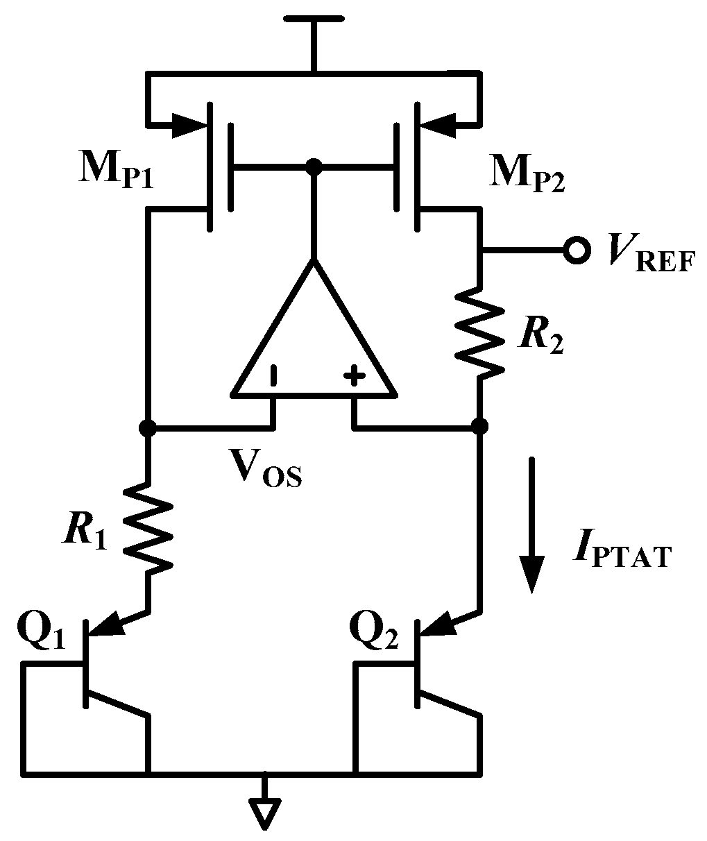
2.1. Error Analysis of the BJT-Based BGR

The key point of this paper is to utilize the techniques of offset cancelling, correlated double sampling and switched-RC to improve the accuracy of the raw BGRs under stringent power consumption constraints. A conventional BJT-based BGR is employed here for demonstration. The core circuit of the BJT-based BGR is shown in Figure 1. The reference voltage generated by it is given by:
V R E F = V B E 2 + R 2 R 1 Δ V B E .
When considering non-ideal factors relevant with VBE and Opamp offset, Equation (1) can be approximately rewritten as
V R E F = V B E 2 + R 2 R 1 ( Δ V B E + V o s )
where the superscript ′ denotes the erroneous quantity. High mismatch characteristic of MOS transistors can introduce considerate offsets to Opamp especially under extreme low power consumption. The VBE spread is also critical because it directly translates an error in VREF. The proposed circuit concentrates on canceling these two sources of errors which have large magnitudes of effects on the accuracy of BGR output voltage.

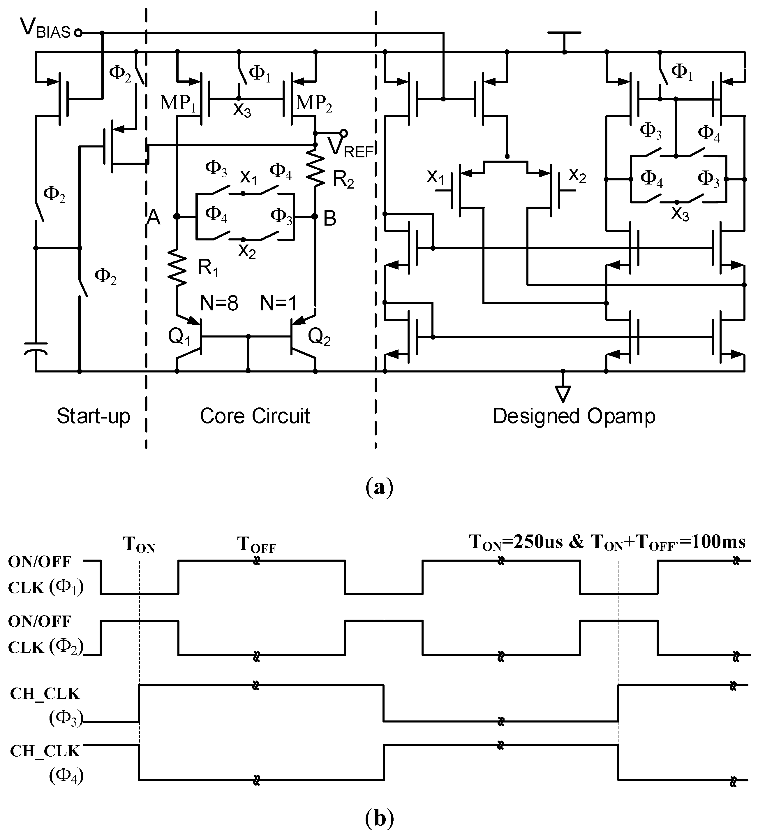
2.2. Architecture of the Proposed BGR Circuit

The systematic architecture of the proposed BGR is shown in Figure 2, which consists of an on-off VBE-based BGR with chopper mechanism, a sampling-capacitor block, and a sample-and-hold switched-RC filter. Also, there is a digital block to generate the low-duty-cycle clocks used in the on-off BGR, which is manually designed as the analog circuits to reduce the turnover rate of the clocks and thus save power. The on-off BGR takes advantages of the conventional VBE-based BGR topology. When consuming dozens of microampere (μA), the conventional VBE-based BGR operates reliably and has little process variation spread. During the hold period, the on-off BGR is turned off to save power. The sampling-capacitor block is based on the technique of correlated double sampling (CDS), which samples twice in a working (on) period, before and after the conversion of the chopper connection state in the on-off BGR, respectively. Therefore, the offset of the Opamp Vos is cancelled out. When the BGR block entered the off state, the switched-RC filter takes the average of the last twice sampled voltages, holds it until next working (on) state, and gets rid of the out-of-band noise through the function of filtering.

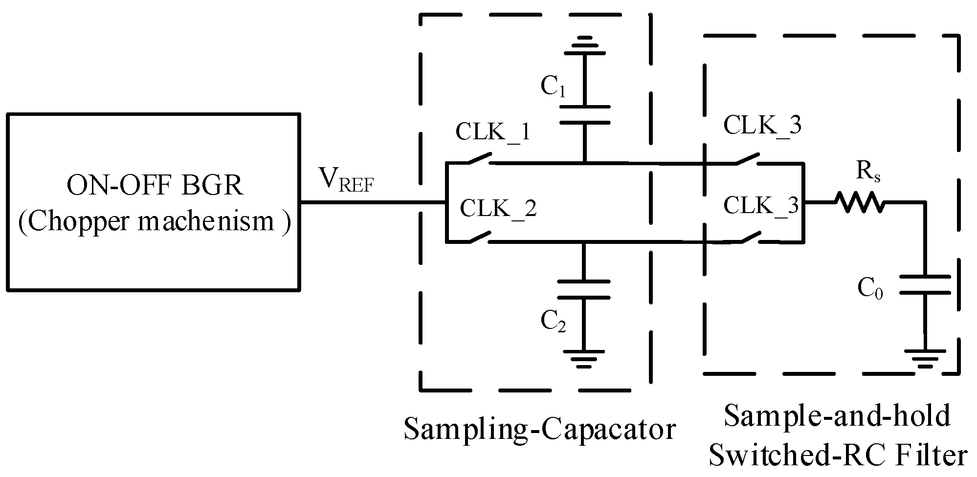
2.3. Chopper Mechanism and Correlated Double Sampling

Figure 3 shows the implementation of the on-off BGR which employs chopper mechanism. A near-zero power consumption start-up structure is adopted. The parameter values of the main components in the BGR core circuit are as follows. The emitter area of Q1 and Q2 is 2 × 2 μm. R1 = 10 kΩ and R2 = 80 kΩ. The size of MP1/2 is 8 μm/16 μm × 6 while the size of the switch transistors is 4 μm/1 μm × 1. The sizes of the transistors are designed to be large for good matching and low flicker noise. Considering the low speed characteristic of the designed circuit, the lengths of the transistors are selected at least 3 times of the 350 nm minimum channel length for lower static leakage current.
Under phase Φ1 and Φ2, the BGR power cycle is controlled by the clock ON/OFF CLK as shown in Figure 3b. With the duty cycle D = 0.25% (TON = 250 us, TON + TOFF = 100 ms), a working current of 16 uA is budgeted for the BGR block to achieve an average power consumption as low as 40 nA. The base-emitter voltage of transistor Q2 is given by
V B E 2 = V T ln ( I C J S A ) ,
where IC and JS are the working collector current and reverse saturation current per unit area of the transistor, respectively, and A is the emitter area. We assume the current variation is IX. Then the relative error can be deduced as in Equation (5).
V B E 2 = V T ln ( I C + I X J S A )
ε = V B E V B E V B E = ln ( I C + I X J S A ) ln ( I C J S A ) 1 1 ln ( I A J S A ) I X D I A ,
where ε represents the relative error, and IA = IC. D is the average current. When the working collector current IC is increased by an on/off duty cycle of 0.25%, the relative error spread of VBE is 400 times less.
The chopper blocks are controlled by the 10Hz CH_CLK to cancel the offset of the Opamp under phases Φ3 and Φ4. In the middle of the on-phase of BGR, the chopper blocks convert connection status from (X2---A, X1---B) to (X1---A, X2---B). In the next on-phase, the connection status changes back. Another chopper block is introduced in the signal path of the designed Opamp to assure that a negative feedback loop be formed according to the chopper status in the on-off BGR.
Figure 4 shows the sampling-capacitor circuit using the technique of correlated double sampling (CDS) [14,15]. The values of the sampling capacitors are selected as C1 = C2 = C0 = 40 μm × 40 μm (1.6 pF). In the control of double sampling clocks CLK_1 and CLK_2, whose clock timings are shown in Figure 4b, C1 and C2 sample the output of the on-off BGR VREF before and after the chopper connection state conversion during TS1 and TS2, respectively, in a working (on) period. C0 samples during the interval TS and sums up the two sampled voltages in it. Using Equation (2), only the Opamp offset is considered,
V 1 = V B E 2 + R 2 R 1 ( Δ V B E + V o s ) = V d e s + R 2 R 1 V o s
V 2 = V B E 2 + R 2 R 1 ( Δ V B E V o s ) = V d e s R 2 R 1 V o s
V 1 C + V 2 C + V 0 C = V 0 * 3 C    If ,   V 0 = V 0 So ,   V 0 = V 1 + V 2 2 = V d e s ,
where C1 = C2 = C0 = C, V1′ is the voltage on C1 which is sampled before the connection state conversion, V2′ is the voltage on C2 sampled after the conversion, V0 is the current voltage on C0 and V0′ is the sample voltage in next cycle on C0. Eventually, Vdes is the original design value of VREF. When the stable condition is reached, V0 is the average value of V1 and V2, canceling the error of VREF caused by the Opamp offset.

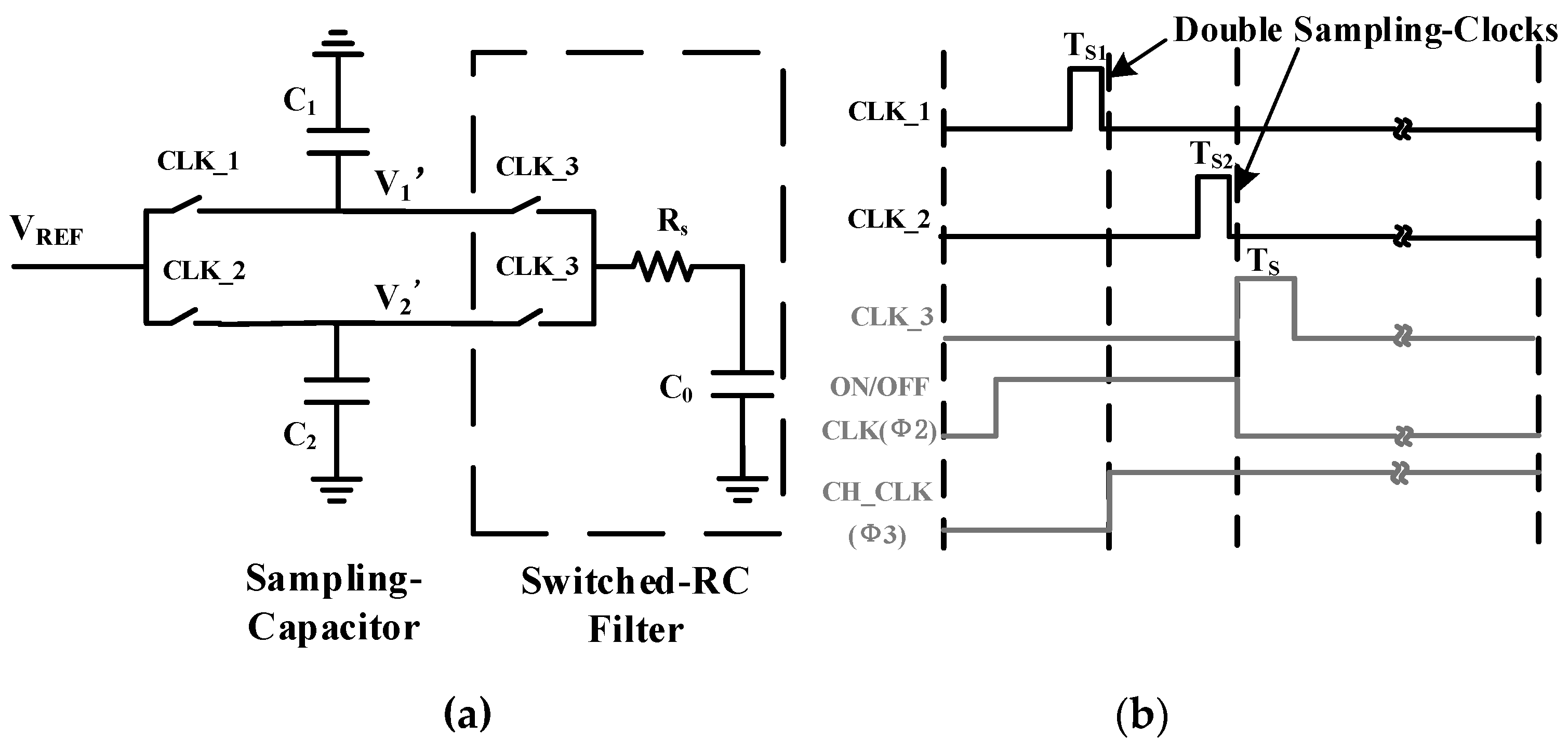
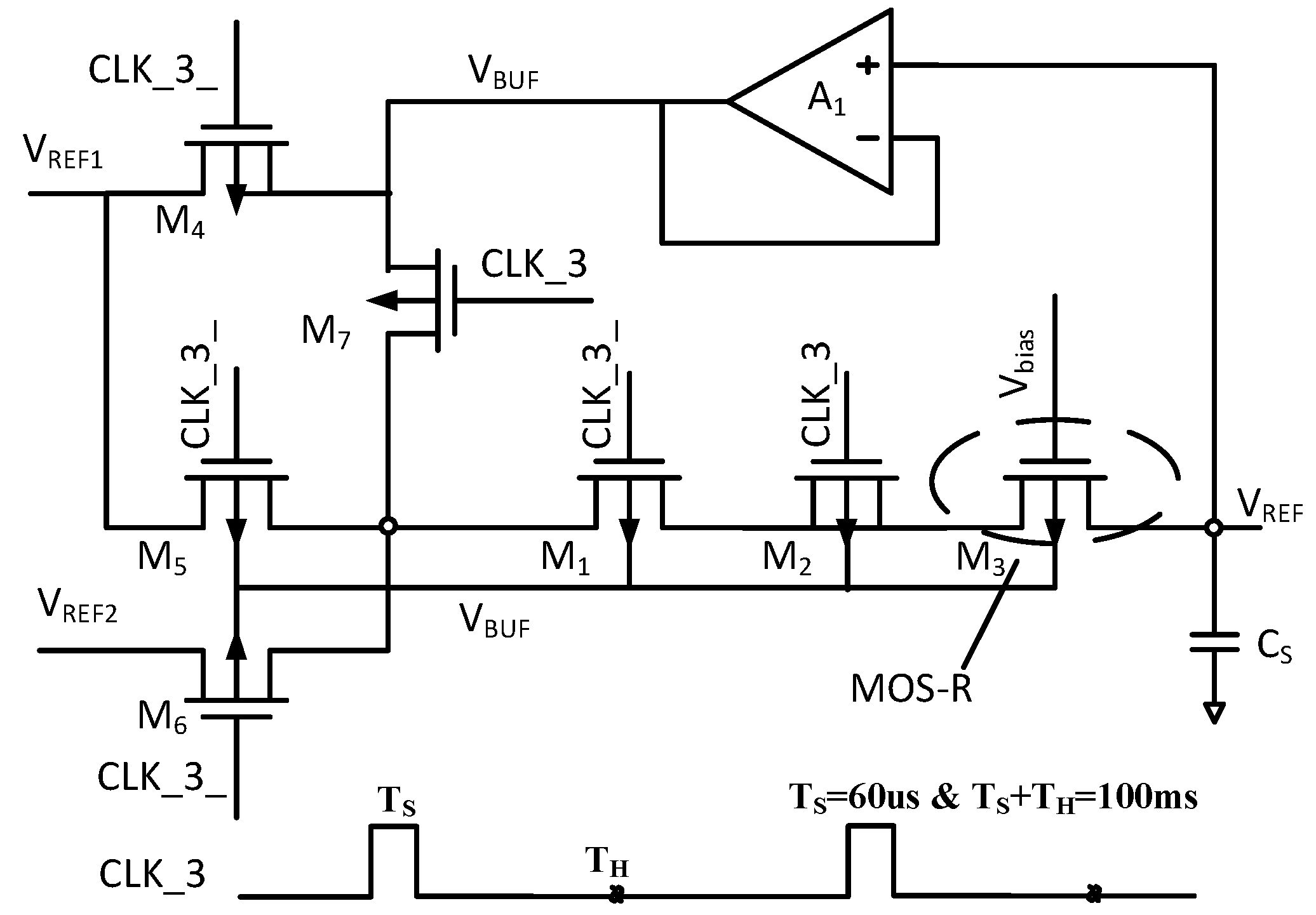
2.4. Sample-and-Hold Switched-RC Filter

Figure 5 shows the circuit implementation of the sample-and-hold switched-RC filter. A MOS-R is used to achieve a high RC filtering resistance of 25 MΩ with small chip area. To alleviate the effect of injection and clock feedthrough, a dummy MOS switch M2 is added in series with the actual switch M1 [13].
Since the drain-bulk and drain-source leakage is critical to the accuracy and stability of VREF output, especially during a long hold time of 100 ms, a simple feedback buffer A1 is used to reduce the voltage drop. In the hold phase, the bulk and source nodes of M1 are buffered to VREF through M7, eliminating charge leakage at CS.
Moreover, the filter emulates a much lower filter pole frequency by pulse-switching them. Compared to the RC filter in Figure 2, the effective pole frequency in Figure 5 is given by [13]:
f L P F = D 2 π R S C S
with CS = 10 pF, RS = 25 MΩ, and D = 0.06% (TS = 60 us, TH + TS = 100 ms), a filter pole of 0.4 Hz can be achieved, which is about two decades lower than the noise integration bandwidth. Consequently, out-of-band noise could be filtered more thoroughly.

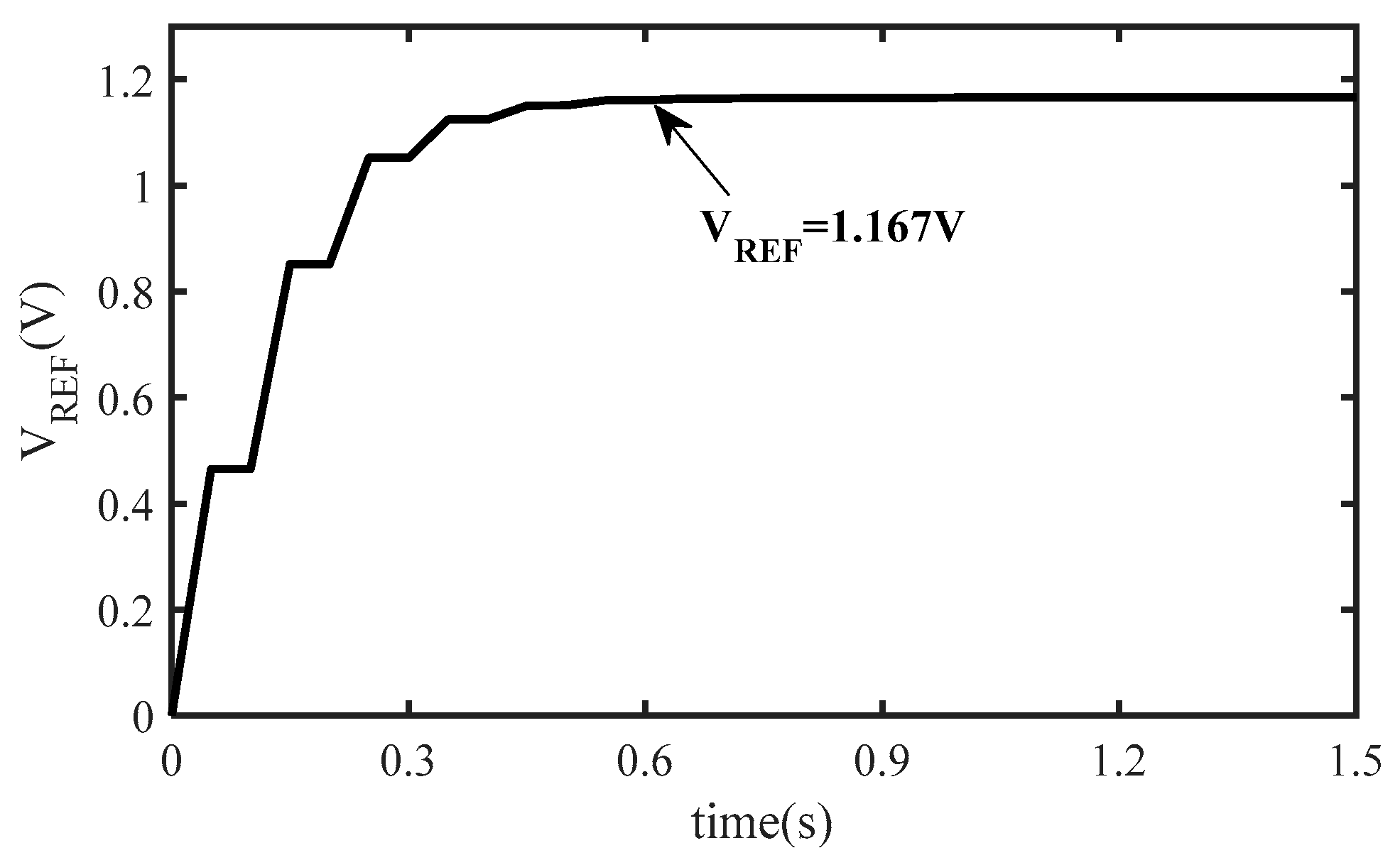
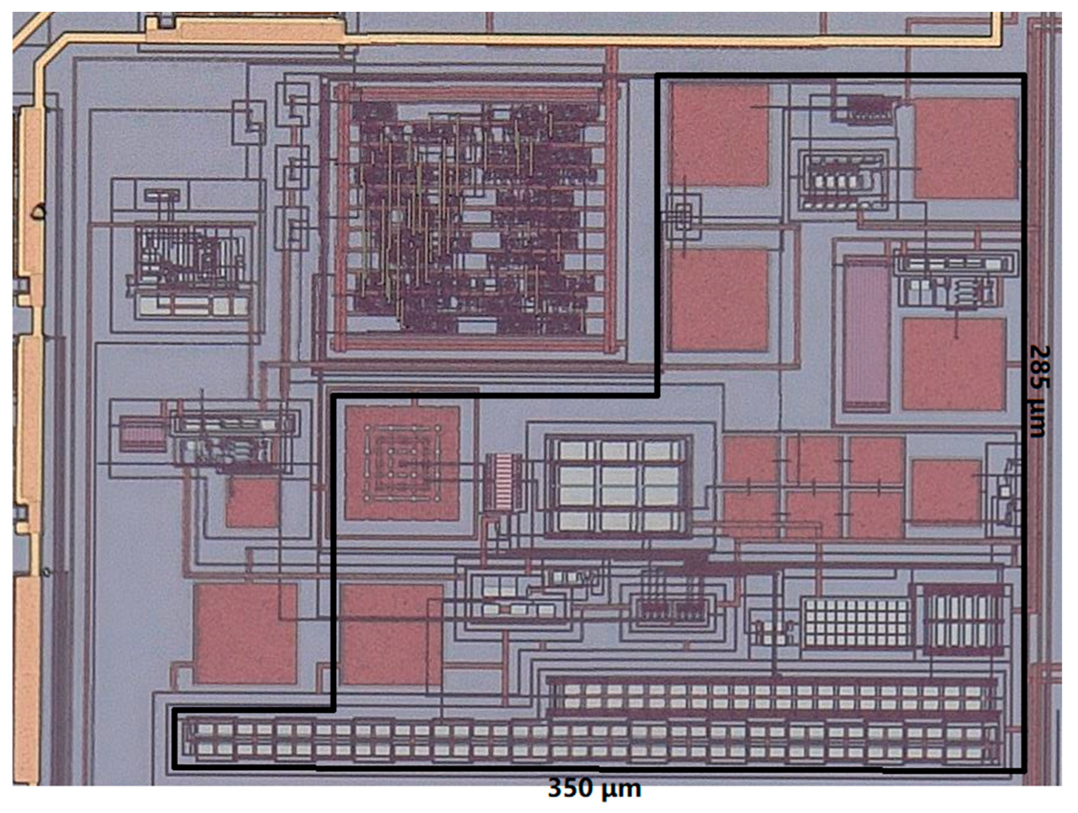
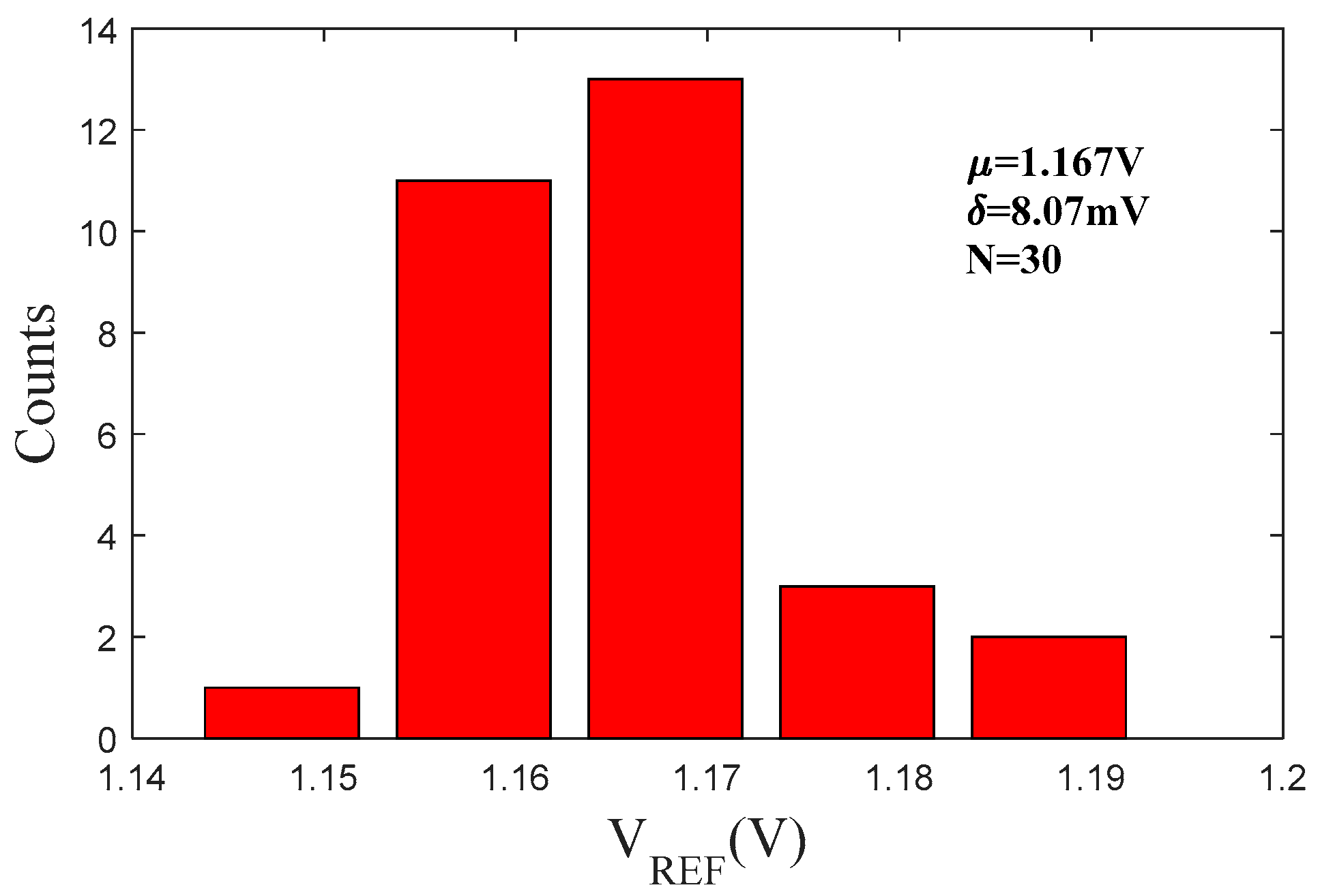
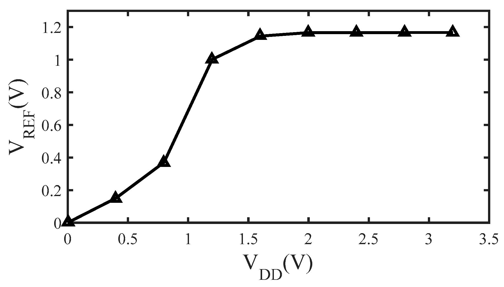
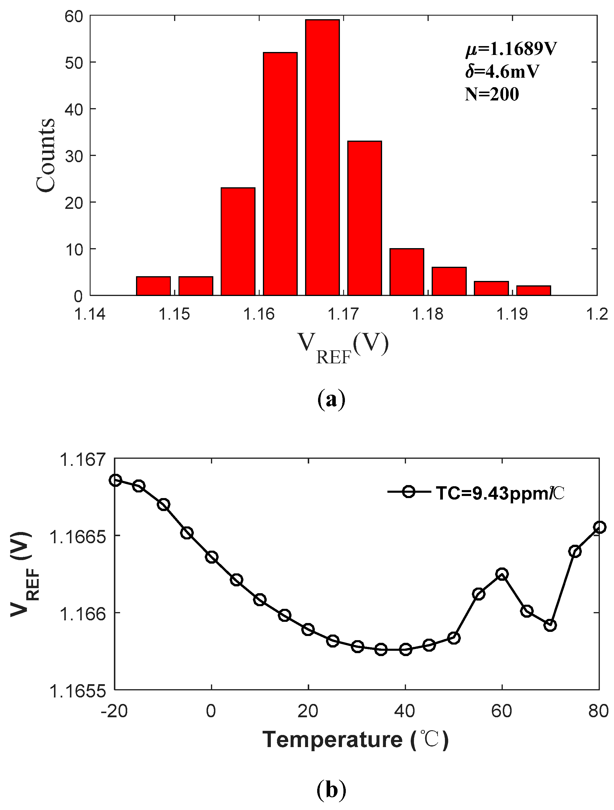
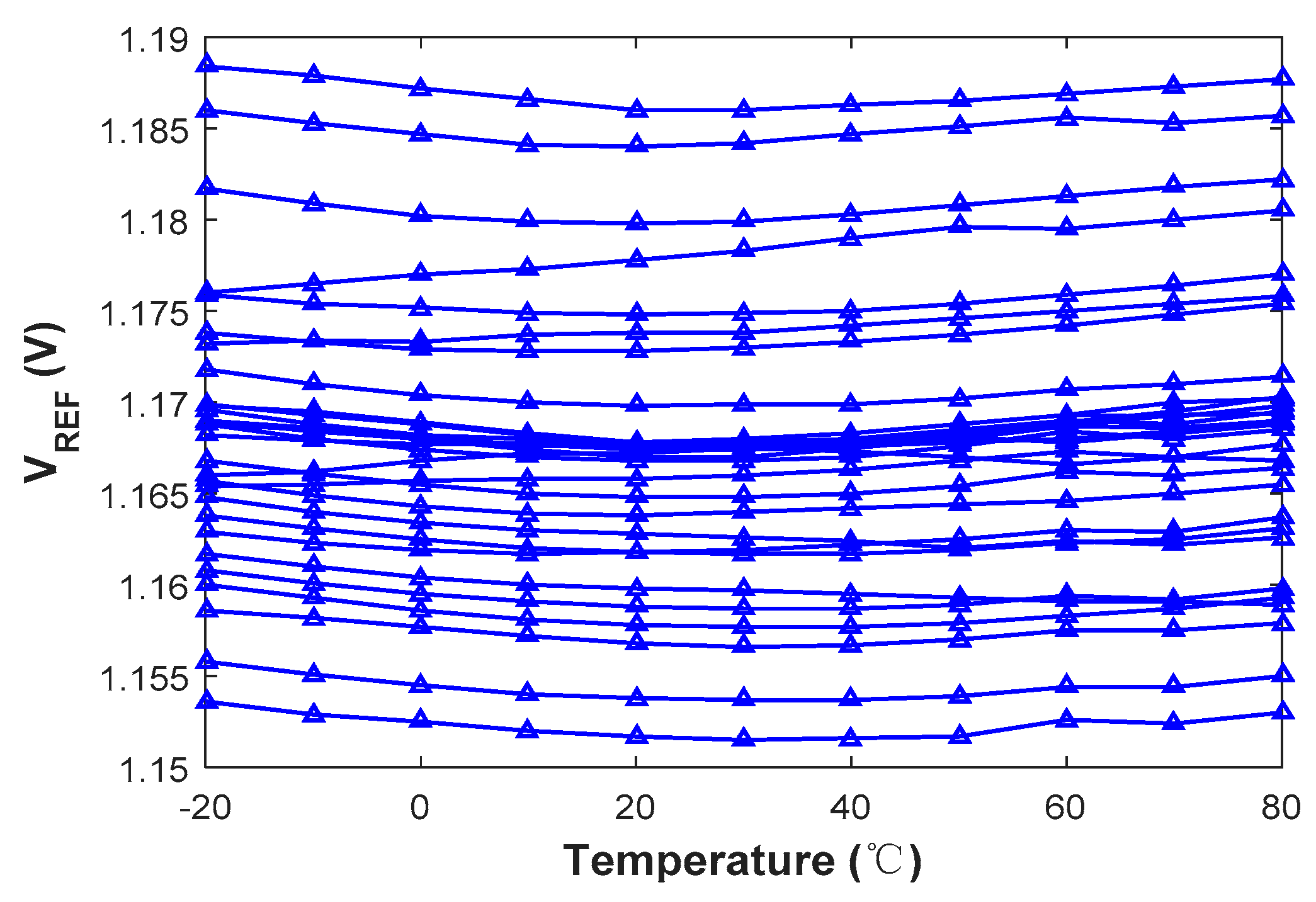
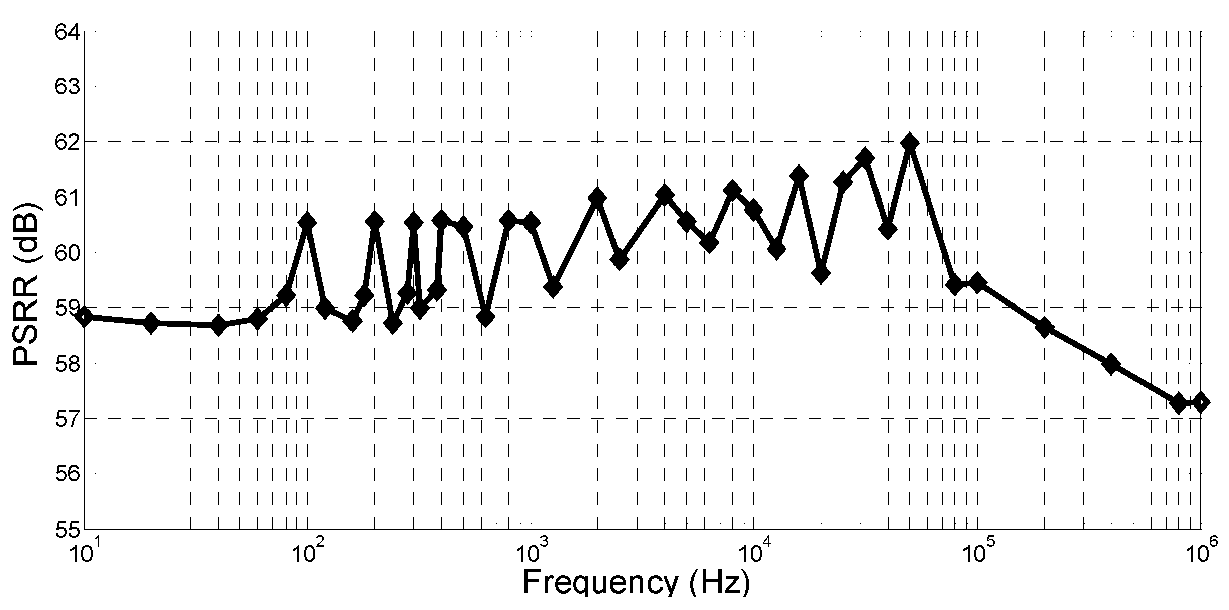
3. Simulation and Measurement Results

The Offset-Cancelation Switched-RC Bandgap Reference presented in this paper has been applied in an implanted cardiac pacemaker ASIC, featured with low power, high reliability and low speed. Consequently, 0.35 μm CMOS technology is employed, which is not advanced but adequately qualified for such applications [1,2]. Also, a lithium-iodine battery with a typical supply voltage of 2.8 V is usually used for cardiac pacemakers, which has a sufficient level of safety and good discharging characteristics [4].
For on-off BGRs with small duty cycles, the settling time for start-up is usually concerned. Figure 6 shows the transient output voltage of the proposed circuit at the supply voltage of 2.8 V and temperature of 27 °C. It takes about 0.6 ms to reach steady state. Monte Carlo 200 simulation runs have been done after layout parasitic extraction, considering the process variation and mismatch. The results are presented in Figure 7a. The mean value (μ) of the proposed BGR is 1.1689 V with the standard deviation (σ) of 4.6 mV, and the coefficient of variation is calculated to be about 0.39%. The simulated temperature dependence of the output reference voltage VREF is plotted in Figure 7b. The temperature coefficient (TC) of the proposed BGR is 9.43 ppm/°C with temperature ranging from −20 to 80 °C.
The proposed BGR circuit is implemented in 0.35 μm standard CMOS process. Figure 8 shows the BGR micrograph of the die. The core circuit occupies an area of 0.063 mm2, which could be optimized after an elaborate layout design. The total current consumption is measured as 78 nA on average from 30 samples. The digital clock generation block consumes 26 nA average current, which means that the percentage of the overhead power consumption by the clock generation block is 33.3% or one third. Figure 9 shows the distribution of the measured output voltage in 30 samples with 2.8 V supply voltage at 27 °C. The mean value (μ) is 1.167 V with the standard deviation (σ) of 8.1 mV. The proposed BGR can achieve an accuracy of 0.69% in the measurement. The accuracy of 0.69% is achieved without trimming and could be considered to be adequate for most implantable biomedical electronics. The low power feature is obtained due to the low duty cycle (D = 0.25%) operation of the on-off BRG. Moreover, the following correlated double sampler and the switched-RC filter just consume about 12 nA average current and occupy about 0.03 mm2 chip area of the total 0.063 mm2 chip area, but guaranteed the good performance of the on-off BRG. The on-off BGR achieves an untrimmed measured accuracy of 0.69%, which is comparable with the accuracy of BGRs with current consumptions of hundreds of times larger, just at a small price.
Figure 10 shows VREF versus temperature ranging from −20 to 80 °C and the measured TC ranges from 13.7 ppm/°C to 38.2 ppm/°C with an average TC of 19.6 ppm/°C. Figure 11 shows the measured reference voltage versus the supply voltage at 27 °C. When the supply voltage changes from 1.8 V to 3.2 V, the BGR voltage variation is less than 0.83 mV. The reference voltage can achieve the line regulation of 0.59 mV/V. For measurement convenience, when measuring the power supply rejection ratio (PSRR), the on-off period is set at 10 ms instead of 100 ms, which will not affect the authenticity of the measured results. Figure 12 shows the PSRR results, which is better than 58.6 dB before 200 kHz. There are peaks at multiples of 100 Hz (1/10 ms) due to the characteristic of sampling. When the frequency of the fluctuation on the supply is the same as the sampling rate, the effect of the supply fluctuation on the sampled output voltage is also the same during the on phase in every sampling period and thus will be attenuated.
The performance of the proposed BGR circuit is summarized in Table 1, and these results are compared with other published references. From Table 1, it is observed that this work has the best line regulation and temperature coefficient in the untrimmed voltage references, while it also has advantages in the aspects of current consumption and untrimmed accuracy. However, the limitations of such on-off BGR are analyzed as follows. First, a small ripple at the switching moment still exists after switched-RC filtering. For continuous-time applications, this issue should be considered. Second, because the BGR output voltage is sampled in the capacitor, it has limited driving ability.

4. Conclusions

An ultra-low power, high accuracy BGR designed for implantable medical electronics is presented in this paper. To solve the conflict between low power and high accuracy, an on-off bandgap combined with sample-and-hold switched-RC filter is developed. A higher working current is allowed to alleviate VBE spread, which directly causes error to output voltage, but also keeps the average power consumption as low as 220 nW with the voltage supply of 2.8 V. Furthermore, to improve the accuracy ulteriorly, the error brought by the Opamp offset is eliminated by applying correlated double sampling strategy. As a result, the measured voltage accuracy of 0.69% is achieved without trimming, which is adequate for most implanted medical electronics. The circuit shows a line regulation of 0.59 mV/V in the supply voltage range of 1.8–3.2 V and a TC of 19.6 ppm/°C in the temperature ranging from −20 to 80 °C. The proposed BGR circuit meets all the requirements of implantable medical electronics. It is very suitable for application in biomedical systems.

Author Contributions

Conceptualization, J.X. and R.Z.; investigation, M.W. and S.W.; writing—original draft preparation, J.X. and Y.W.; writing—review and editing, G.Z. and C.-F.Y.; project administration, R.Z.

Funding

This research was funded by National Natural Science Foundation of China (Grant No. 61774126), Core Electronic Devices, High-end General Chips and Basic Software Products Projects of China (Grant No. 2017ZX01030204), and the Fundamental Research Funds for the Central Universities.

Conflicts of Interest

The authors declare no conflict of interest.

References

  1. Zhang, J.; Zhang, H.; Zhang, R.; Xu, J.; Yang, Z.; Zhang, M.; Li, J. A mixed-signal ASIC for triple-chamber cardiac pacemakers with heart resistance measurement. In Proceedings of the 2015 IEEE Asian Solid-State Circuits Conference (A-SSCC), Xiamen, China, 9–11 November 2015; pp. 33–36. [Google Scholar]
  2. Zhang, J.; Zhang, H.; Xu, J.; Zhao, Y.; Li, J.; Hu, G.; Wang, J.; Zhang, R.; Lian, Y. A low energy ASIC for triple-chamber cardiac pacemakers with contact resistance measurement. Microelectron. J. 2017, 60, 65–74. [Google Scholar] [CrossRef]
  3. Swampillai, J.; Stiles, M.K. Hazards of modern pacemaker programming: Less is more. J. Electrocardiol. 2013, 46, 140. [Google Scholar] [CrossRef] [PubMed]
  4. Fayomietal, C.J.B. Sub-1-V CMOS Bandgap Reference Design Techniques: A Survey. Analog Integr. Circuits Signal Process. 2010, 62, 141–157. [Google Scholar]
  5. Peng, K.; Xu, Y. Design of Low-Power Bandgap Voltage Reference for IoT RFID Communication. In Proceedings of the 2018 IEEE 3rd International Conference on Integrated Circuits and Microsystems (ICICM), Shanghai, China, 24–26 November 2018; pp. 345–348. [Google Scholar]
  6. Wu, C.; Goh, W.L.; Yang, Y.; Chang, A.; Zhu, X.; Wang, L. A start-up free 200nW bandgap voltage reference. In Proceedings of the 2016 14th IEEE International New Circuits and Systems Conference (NEWCAS), Vancouver, BC, Canada, 26–29 June 2016; pp. 1–4. [Google Scholar]
  7. Souliotis, G.; Plessas, F.; Vlassis, S. A high accuracy voltage reference generator. Microelectron. J. 2018, 75, 61–67. [Google Scholar] [CrossRef]
  8. Andreou, C.M.; Georgiou, J. A 0.7 V, 2.7 µW, 180 °C Temperature Range, 12.9 ppm/°C, 0.023 mm2, Subthreshold Voltage Reference. Int. J. Circuit Theory Appl. 2017, 45, 1349–1368. [Google Scholar] [CrossRef]
  9. Sarpeshkar, R. Ultra Low Power Bioelectronics; Cambridge University Press: Cambridge, UK, 2010. [Google Scholar]
  10. Ueno, K.; Hirose, T.; Asai, T.; Amemiya, Y. A 300 nW, 15 ppm/°C, 20 ppm/V CMOS Voltage Reference Circuit Consisting of Subthreshold MOSFETs. IEEE J. Solid-State Circuits 2009, 44, 2047–2054. [Google Scholar] [CrossRef]
  11. Abbasi, M.U.; Raikos, G.; Saraswat, R.; Rodriguez-Villegas, E.; Usaid, A.M. A high PSRR, ultra-low power 1.2V curvature corrected Bandgap reference for wearable EEG application. In Proceedings of the 2015 IEEE 13th International New Circuits and Systems Conference (NEWCAS), Grenoble, France, 7–10 June 2015; pp. 1–4. [Google Scholar]
  12. Mu, J.; Liu, L.; Zhu, Z.; Yang, Y. A 0.5 V, 40 nW voltage reference for WBAN devices. In Proceedings of the 2016 IEEE Biomedical Circuits and Systems Conference (BioCAS), Shanghai, China, 17–19 October 2016; pp. 504–507. [Google Scholar]
  13. Magod, R.; Suda, N.; Ivanov, V.; Balasingam, R.; Bakkaloglu, B. A Low-Noise Output Capacitorless Low-Dropout Regulator with a Switched-RC Bandgap Reference. IEEE Trans. Power Electron. 2017, 32, 2856–2864. [Google Scholar] [CrossRef]
  14. Hafiz, O.A.; Wang, X.; Hurst, P.J.; Lewis, S.H. Immediate Calibration of Operational Amplifier Gain Error in Pipelined ADCs Using Extended Correlated Double Sampling. IEEE J. Solid-State Circuits 2013, 48, 749–759. [Google Scholar] [CrossRef]
  15. Son, S.; Jeon, S.; Namgung, S.; Yoo, J.; Song, M.; Suho, S. A one-shot digital correlated double sampling with a differential difference amplifier for a high speed CMOS image sensor. In Proceedings of the 2015 IEEE International Symposium on Circuits and Systems (ISCAS), Lisbon, Portugal, 24–27 May 2015; pp. 1054–1057. [Google Scholar]
  16. Jiang, J.; Shu, W.; Chang, J.S. A 5.6 ppm/°C Temperature Coefficient, 87-dB PSRR, Sub-1-V Voltage Reference in 65-nm CMOS Exploiting the Zero-Temperature-Coefficient Point. IEEE J. Solid-State Circuits 2017, 52, 623–633. [Google Scholar] [CrossRef]
  17. Wang, Y.; Zhu, Z.; Yao, J.; Yang, Y. A 0.45-V, 14.6-nW CMOS Subthreshold Voltage Reference With No Resistors and No BJTs. IEEE Trans. Circuits Syst. 2015, 62, 621–625. [Google Scholar] [CrossRef]
  18. Shrivastava, A.; Craig, K.; Roberts, N.E.; Wentzloff, D.D.; Calhoun, B.H. A 32 nW bandgap reference voltage operational from 0.5 V supply for ultra-low power systems. In Proceedings of the 2015 IEEE International Solid-State Circuits Conference (ISSCC) Digest of Technical Papers, San Francisco, CA, USA, 22–26 February 2015; pp. 1–3. [Google Scholar]
  19. Basyurt, P.B.; Bonizzoni, E.; Aksin, D.Y.; Maloberti, F. A 0.4-V Supply Curvature-Corrected Reference Generator with 84.5-ppm/°C Average Temperature Coefficient within 40 °C to 130 °C. IEEE Trans. Circuits Syst. 2017, 64, 362–366. [Google Scholar] [CrossRef]
Figure 1. The basic topology of the bipolar junction transistor (BJT)-based bandgap reference (BGR) core circuit.
Electronics 08 00814 g001
Figure 2. Block diagram of the proposed BGR.
Electronics 08 00814 g002
Figure 3. (a) Proposed on-off BGR with chopper mechanism; (b) Control clocks for BGR power cycle and chopper blocks.
Electronics 08 00814 g003
Figure 4. (a) Proposed sampling-capacitor circuit along with switched-RC block; (b) Control clocks for sampling switches.
Electronics 08 00814 g004
Figure 5. Proposed sample-and-hold switched-RC filter circuit and control clock timing.
Electronics 08 00814 g005
Figure 6. The output voltage of the proposed circuit.
Electronics 08 00814 g006
Figure 7. (a) 200 Monte Carlo simulation results. (b) Temperature coefficient simulation at 2.8 V supply.
Electronics 08 00814 g007
Figure 8. Microphotograph of BGR chip.
Electronics 08 00814 g008
Figure 9. Measured results for 30 samples.
Electronics 08 00814 g009
Figure 10. Measured reference voltage versus temperature for 30 samples.
Electronics 08 00814 g010
Figure 11. Measured reference voltage versus the supply voltage.
Electronics 08 00814 g011
Figure 12. Measured power supply rejection ratio (PSRR).
Electronics 08 00814 g012
Table 1. Comparison table.
Parameter[16][17][18][19]This Work
Process65 nm180 nm130 nm180 nm350 nm
Publication YearJSSC 2017TCAS-II 2015ISSCC 2015TCAS-II 20172019
Accuracy (σ/µ)0.39%(T)3.9%(UT)0.67%(UT)2%(T),10.69%(UT)
TypeVTHVTHVBEVTHVBE
TC (ppm/℃)5.6(T)64(T)75(UT)84.5(UT)19.6(UT)
Supply0.8 V0.45 V0.5 V0.4 V2.8 V
Output Voltage428 mV120 mV500 mV212 mV1.17 V
Current Consumption16.3 μA32.4 nA64 nA480 nA78 nA
Line regulation1 mV/V1.2 mV/V10 mV/V2 mV/V0.59 mV/V
(T): trimmed. (UT): untrimmed. 1: 3σ.

