


Abstract
The performance of true random number generators (TRNGs) fundamentally depends on the quality of their entropy sources (ESs). However, many FPGA-friendly designs still rely on a single mechanism and struggle to achieve both high throughput and low resource cost. To address this challenge, we propose the exclusive OR (XOR) Self-Feedback Ring Oscillator (XORSFRO), an XORNOT-style TRNG that integrates two cross-connected XOR gates with a short inverter delay chain and clocked sampling. A unified timing model is developed to describe how arrival-time skew and gate inertial delay lead to cancellation, narrow-pulse generation, and inversion events, thereby enabling effective entropy extraction. Experimental results on Xilinx Spartan-6 and Artix-7 FPGAs demonstrate that XORSFRO maintains stable operation across standard process–voltage–temperature (PVT) variations, while achieving higher throughput and lower hardware overhead compared with recent FPGA-based TRNGs. The generated bitstreams pass both the NIST SP 800-22 and NIST SP 800-90B test suites without post-processing.
1. Introduction
The rapid expansion of distributed photovoltaic (PV) systems has created new opportunities for clean energy generation [1,2]. According to recent projections, the global penetration of PV installations will continue to accelerate, bringing substantial economic and environmental benefits [3,4,5]. At the same time, these systems are increasingly networked, often integrated into smart grids or remote monitoring infrastructures, forming a large-scale distributed internet-of-things (IoT) platform. However, such connectivity exposes PV systems to significant cybersecurity risks, including the compromise of cryptographic keys and the interception of secure communication channels. Therefore, ensuring reliable security mechanisms has become a critical requirement for distributed PV deployments [6,7,8,9].
Random numbers are the cornerstone of cryptographic security, serving as the foundation for key generation and authentication protocols [10,11,12,13,14,15,16]. However, in distributed photovoltaic systems, the challenge is even greater: Many edge devices are resource-constrained and deployed in environments with fluctuating power supply and limited computational capacity. Conventional cryptographic primitives often impose excessive hardware and energy overhead, rendering them impractical for these platforms. Thus, a lightweight, energy efficient and high quality TRNG is essential to protect the security of distributed photovoltaic systems.
Random numbers can be classified into pseudorandom and true random sequences [17,18,19,20]. Pseudorandom numbers are generated by deterministic algorithms seeded with initial values. Although efficient, they exhibit periodicity and predictability, making them vulnerable to adversarial exploitation [2,21,22,23]. By contrast, TRNGs extract entropy from physical processes to produce non-reproducible and unpredictable sequences. On FPGAs, TRNGs typically consist of three main components: the entropy source (ES), which converts physical noise into digital randomness; the entropy extractor (or conditioning component), which enhances randomness quality through mechanisms like feedback and mixing; and an optional post-processing unit, which mitigates statistical bias [13,24]. However, environmental variations such as supply voltage, temperature, and external noise can introduce correlation and degrade entropy quality [3,25]. Post-processing methods, such as von Neumann correctors or cryptographic hashing, are widely applied to compensate for these defects, though they also increase design complexity.
Till now, a variety of ES circuits have been explored, including ring oscillators (ROs) [4,18,24], self-timed rings (STRs) [6,7,20,26], digital clock managers (DCMs) [8,10,27], and metastability-based circuits [11,23,28]. While effective, each approach has trade-offs. STRs are robust but complex to control; DCMs add overhead and are absent in many edge-grade devices; metastability-based designs require careful manual routing to ensure sufficient entropy. RO-based TRNGs, which rely on oscillator phase noise and timing jitter, are appealing for their simplicity and small gate count. However, conventional designs often combine multiple ROs through XOR trees to improve statistical quality [12], which increases resource usage and reduces throughput. Moreover, inverter-based ROs require an odd number of inversions to sustain oscillation, limiting design flexibility.
To overcome these limitations, this work introduces a lightweight and high-throughput TRNG architecture, named XORSFRO TRNG. The proposed design augments a conventional RO by mixing its output with a high-speed clock and feeding the result back into the oscillator. This structure enhances ES quality while maintaining low hardware and power overhead, making it well-suited for distributed PV systems that demand both efficiency and security. In particular, the key contributions of this paper are as follows:
- (1)
- We refine the standard RO and propsoe a compact, resource-efficient, and stable self-feedback structure, named XORSFRO, as ES for TRNG.
- (2)
- By feeding back the XOR of a high-speed clock and the RO output, the ES is continuously refreshed, thereby improving minimum entropy and reducing bias.
- (3)
- A two-round cross-serial XOR tree is utilized to prevent the detrimental effects of clock coupling of ES architecture, further improving the randomness.
- (4)
- We establish a mathematical model that explains how input-arrival skew and gate inertial delay generate narrow pulses and inversions, effectively amplifying randomness.
- (5)
- Experimental results on FPGA platforms demonstrate that XORSFRO achieves high throughput and low hardware/power cost, while maintaining robustness across process–voltage–temperature (PVT) variations, making it a strong candidate for secure distributed PV applications.
2. Background
Owing to its structural simplicity and seamless integration into digital ASICs and FPGAs, the RO has become one of the most widely used ES circuits in TRNGs. An RO consists of a closed loop with an odd number of inverters, which sustains oscillation and produces a square-wave output signal. Ideally, the oscillation period remains constant. However, in practice, intrinsic thermal noise, shot noise, and external disturbances such as supply fluctuations introduce jitter, which appears as phase noise in the frequency domain. This jitter forms the physical basis of the randomness in RO outputs.
The design of RO-based TRNGs centers on exploiting and balancing this jitter. Increasing the number of inverters enhances entropy quality but reduces oscillation frequency, thereby limiting throughput. Conversely, reducing the inverter count increases throughput at the cost of randomness. As a compromise, many designs employ multiple ROs in parallel, combining their outputs through an XOR tree to improve both throughput and statistical quality. For instance, Mei et al. achieved a throughput of 160 Mbps using such a structure, though with significant hardware overhead (25 LUTs and 37 DFFs) [13]. A deeper challenge, however, lies in the inherently narrow jitter range of ROs, which makes efficient entropy extraction difficult. Early methods illustrate this trade-off: Sivaraman et al. proposed a beat-frequency detection scheme that digitized phase differences between two ROs using counters, but at the cost of high resource consumption (539 DFFs) and power overhead [14]. Xu et al. introduced an edge-tracing method that improved throughput to 127 Mbps, yet its heavy resource usage and strong sensitivity to PVT variations limited practicality [15].
Recent research has therefore shifted toward refining the circuit structure of RO as ES itself to enhance throughput, reduce resource overhead, and improve robustness. Tao et al. embedded nonlinear feedback units into ROs to amplify inherent unpredictability, achieving 200 Mbps throughput with ultra-low power consumption, though with less-than-ideal resource utilization [17]. Cui et al. designed a multi-stage feedback structure that sampled a PLL clock with RO jitter, broadening the range of entropy extraction and improving both throughput and efficiency, but at the cost of high power consumption [18]. Peng et al. proposed an FPGA-based TRNG leveraging the metastability of RO-driven shift registers, where metastable states simplified entropy extraction and delivered high throughput with minimal resource usage [19].
Beyond these approaches, researchers have explored further architectural modifications to overcome the trade-offs of conventional ROs. Della Sala et al. presented an ultracompact TRNG using latched ROs, which required only 4 LUTs and 3 DFFs but suffered extremely low throughput (0.76 Mbps) [23]. Lin et al. proposed a Galois RO with an event sample architecture, which achieves high throughput and robustness on FPGA platforms [24]. Wu et al. designed a TRNG based on delay chain feedback loops, reaching 150 Mbps throughput, but at the expense of nearly 300 LUTs [29]. More recently, Frustaci et al. employed metastability combined with clock managers, enabling very high throughput (300 Mbps) while still requiring non-negligible hardware cost [11]. These examples highlight the ongoing challenge of balancing throughput, entropy quality, and hardware efficiency.
In summary, an effective TRNG must combine high entropy quality and throughput with low resource and power consumption, while maintaining robustness across PVT variations. Enhancing the ES architecture itself is thus a promising path toward meeting these requirements. Building on this idea, this work introduces an optimized RO-based ES architecture that addresses the limitations of prior approaches while achieving improved performance and efficiency.
3. The Proposed XORSFRO TRNG Architecture
This section introduces the core architecture of the proposed XORSFRO TRNG design. The aim is to achieve a lightweight yet high-quality XORSFRO ES circuit suitable for PV devices.
3.1. XORSFRO Structure
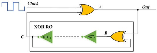
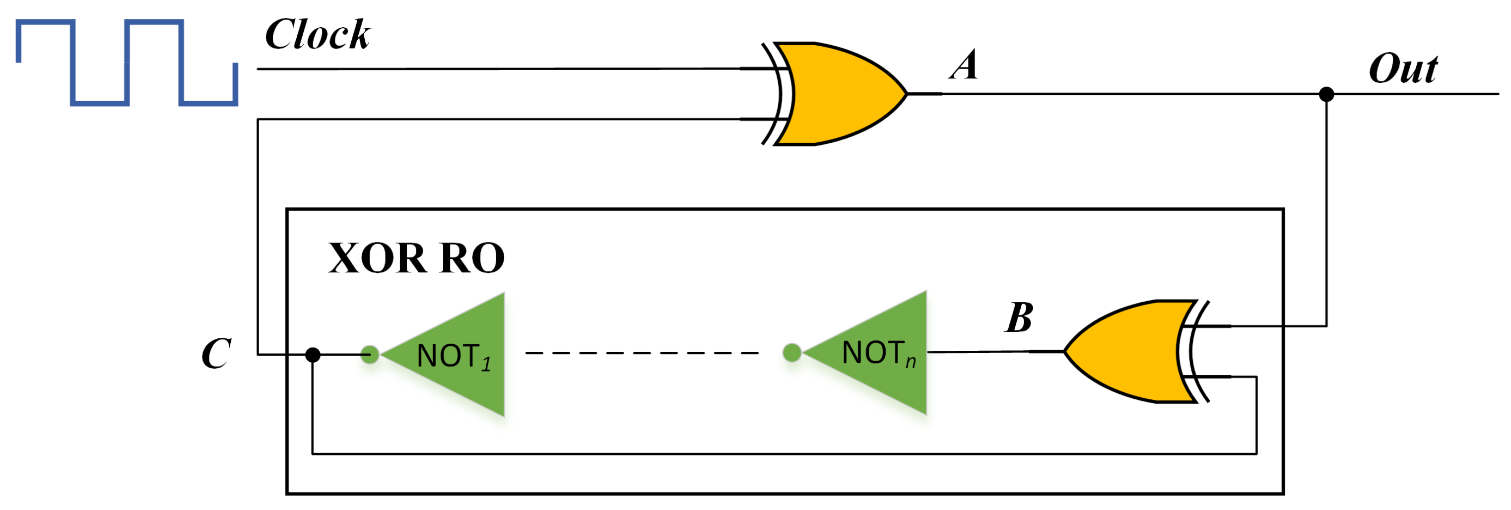
Figure 1 presents the proposed XORSFRO structure. As can be seen from Figure 1, the circuit is highly compact and very simple, using only XOR and NOT gates. Since using a standalone RO as the ES circuit in a TRNG fails to adequately overcome performance limitations, our design integrates an XOR gate with an n-stage RO, as depicted in Figure 1. The XOR gate takes as inputs a clock signal and the output of the XOR-based RO; its output produces a one-bit random sequence. The XOR RO itself consists of inverters and XOR gates. The output signal from this structure is XORed with a clock signal generated by a phase-locked loop (PLL), resulting in the final random bitstream. Moreover, the generated random bit is fed back into the ring oscillator, enabling real-time dynamic control of its oscillation state.
Figure 1.
Basic XORSFRO Structure.
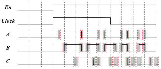
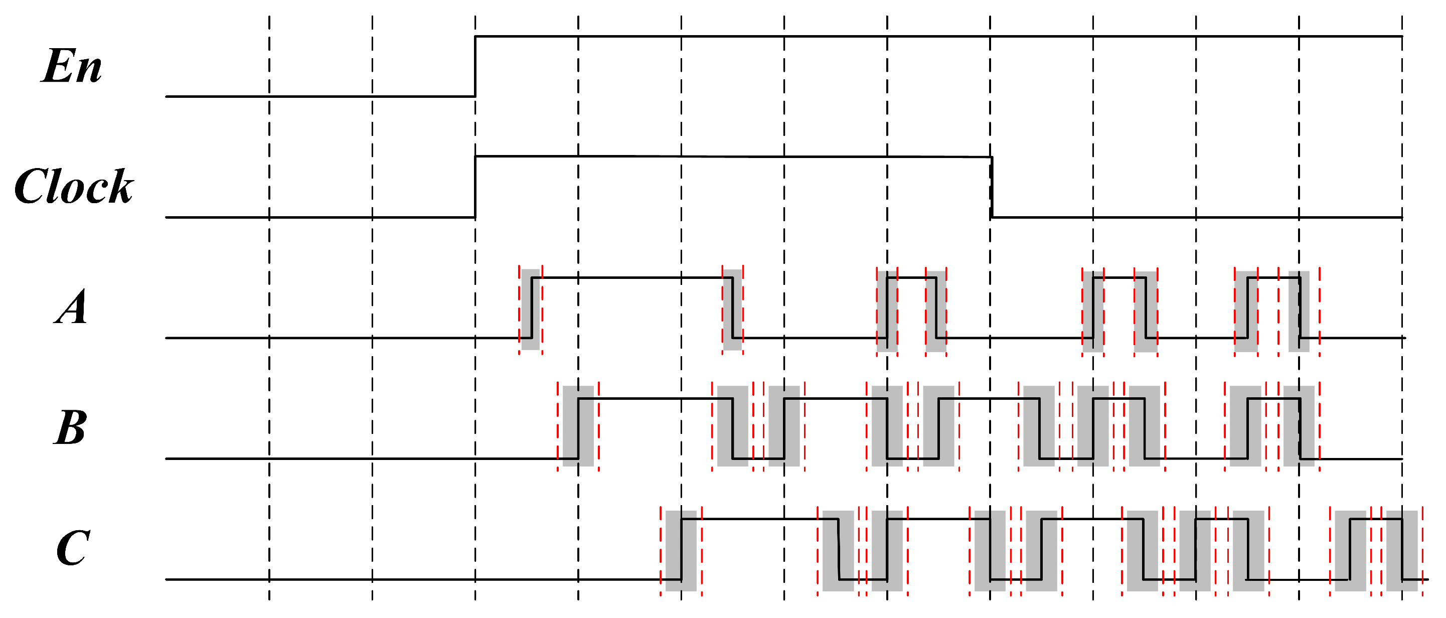
As shown in Figure 2, the timing behavior of the XORSFRO arises from the interaction between the RO transition and the high-speed clock. When their edges arrive nearly simultaneously at the upper XOR gate, the output remains unchanged due to cancellation. Routing skew and feedback perturbation introduce small arrival-time offsets, shifting the effective sampling instant and causing the transition boundaries of nodes A, B, and C to drift across cycles. The spreading of these boundaries and the associated uncertainty regions illustrate how delay imbalance and feedback disturbance induce phase variation in the RO loop. When the arrival-time difference becomes sufficiently large, the XOR output follows either the RO transition or the clock, yielding inverted or non-inverted segments.
Figure 2.
XORSFRO timing waveform.
This repeated evolution of near-alignment, phase drift, and feedback-induced variation broadens the jitter distribution and strengthens the entropy of the XORSFRO.
3.2. XORSFRO TRNG Design
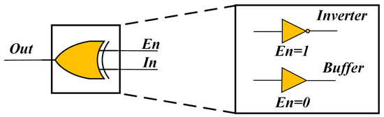
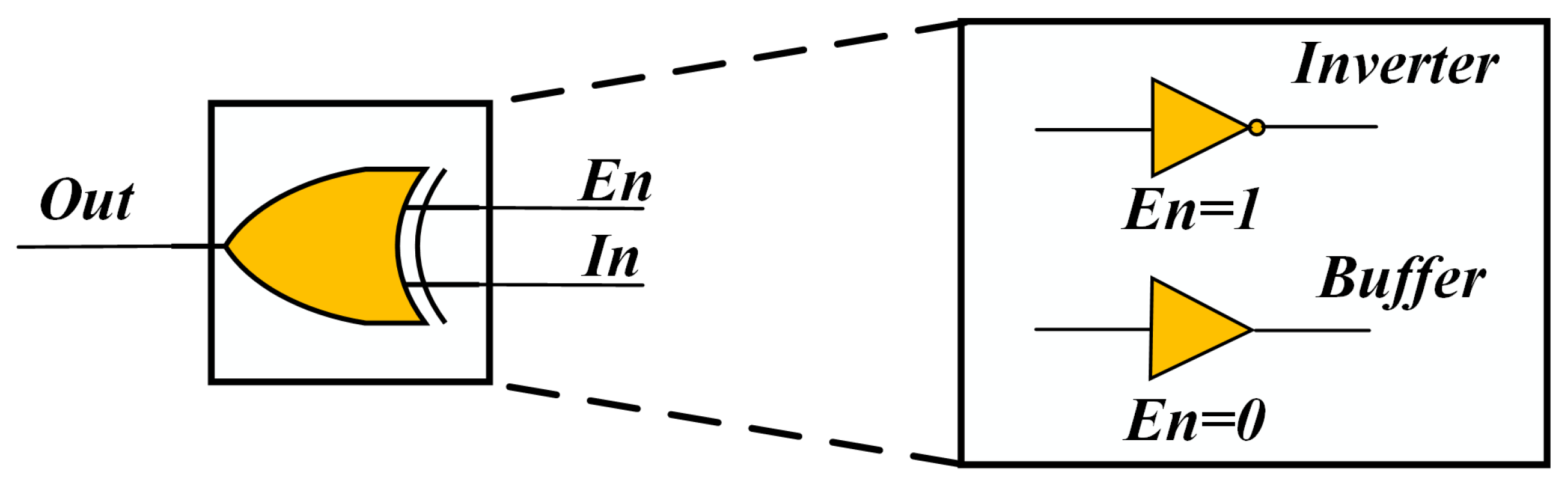
A conventional RO is formed by connecting an odd number of inverters in a closed loop, which restricts flexibility in resource utilization. To overcome this constraint, we replace the inverters (or in some designs, NAND gates) with XOR gates. This modification removes the parity constraint: the RO can now oscillate with either an even or odd number of inverting stages. As shown in Figure 3, when the enable signal En is 1, the XOR gate behaves as an inverter; when En is 0, it acts as a buffer. For example, in an RO with 2n inverters, setting En = 1 makes the XOR serve as an inverter, completing the loop with an odd number of inversions and enabling oscillation. Conversely, oscillation halts when En = 0. Similarly, for an RO with 2n + 1 inverters, setting En = 0 configures the XOR as a buffer, permitting oscillation; otherwise, the loop effectively contains an even number of inversions and oscillation ceases. The same principle applies to the XOR gate that combines the RO output with the PLL clock: it functions as an inverter when the clock is high and as a buffer when the clock is low, thereby dynamically altering the effective number of inversions in the loop.
Figure 3.
XOR gate configurations: inverter vs. buffer.
Feedback structures are known to enhance phase noise in TRNG circuits, thereby improving entropy quality. Simultaneously, XOR operations help improve randomness by combining multiple random sources and reducing bias between ‘0’ and ‘1’. Accordingly, we introduce a feedback mechanism into the RO circuit. This structure comprises an XOR gate and a high-speed clock signal: one input of the XOR is connected to the output of the XOR RO, and the other to the clock. The output of the XOR is used not only as the TRNG output but also fed back into the oscillator, performing continuous XOR mixing that perturbs the oscillation pattern and enhances entropy randomness.
As illustrated in Figure 4, the output of the XOR gate drives both the TRNG output and the oscillator input. The shaded regions indicate intervals where the RO is enabled and free-running oscillations occur. Variations in oscillation duration enlarge the jitter region, shortening the time needed for jitter accumulation. The unshaded regions represent periods when the RO is disabled, during which it essentially behaves as a delay line.
Figure 4.
XOR-based feedback structure combining RO output and high-speed clock for entropy enhancement.
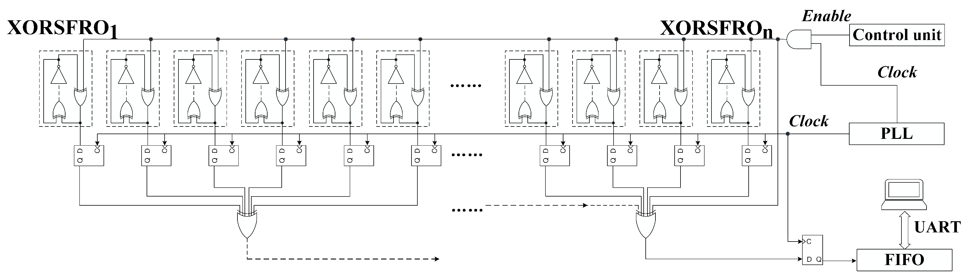
To clarify the feedback and mixing mechanism at the system level, Figure 5 illustrates the proposed XORSFRO TRNG. Each XORSFRO block consists of an XOR-based ring oscillator and a DFF for synchronized sampling. Multiple blocks operate in parallel, and their sampled outputs are combined through XOR networks. The system clock (Clk) from the PLL drives both the DFFs and the improved XOR tree.
Figure 5.
Circuit schematic of the proposed XORSFRO TRNG architecture.
Instead of using a simple inverter-only ring, we insert cross-XOR perturbation paths between internal RO nodes. These internal XOR stages mix two nodes of the ring, introducing controlled phase disturbances that dynamically alter the delay states. As a result, small variations caused by thermal noise, supply fluctuations, and routing mismatches are effectively amplified into measurable jitter and metastability.
From a randomness perspective, the feedback signal serves three roles: (i) disturbing phase alignment to prevent stable oscillation, (ii) sustaining narrow glitches by feeding them directly back into the loop rather than filtering through long inverter chains, and (iii) reducing bias thanks to the balanced property of XOR.
Thus, the feedback path in Figure 5, which originates from the output of each DFF and is re-injected into its corresponding oscillator loop, continuously perturbs the oscillation dynamics. This feedback-driven mixing mechanism effectively increases the entropy density per cycle and enables the generation of high-quality random numbers with minimal hardware overhead.
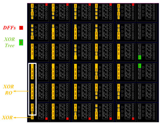
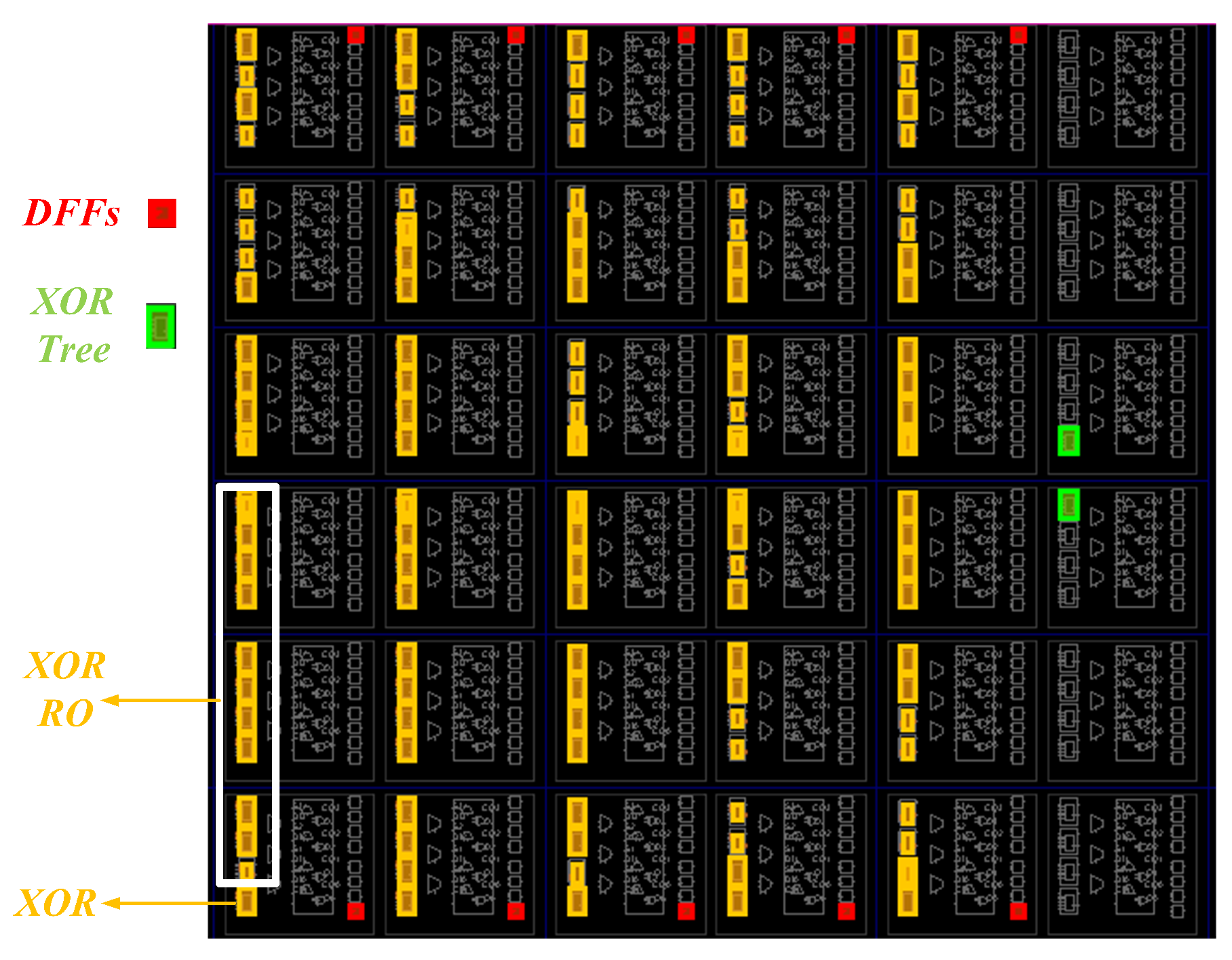
At the physical design level, the FPGA implementation relies entirely on the tools’ automatic placement and routing rather than manually enforced symmetric constraints. As shown in Figure 6, the compiler naturally arranges the XOR-RO chain as a vertically aligned column of LUTs, with the DFFs and XOR-tree elements distributed across neighboring slices. This placement pattern reflects inherent device-level delay imbalance and routing variability, both of which contribute to arrival-time skew in the feedback loop.
Figure 6.
Internal slice connection view of the FPGA compiler.
Instead of attempting to equalize delays through manual routing—which often reduces entropy by suppressing natural jitter—the design leverages these automatically generated mismatches. The slight differences in LUT-to-LUT and inter-slice wiring delays continuously perturb the oscillator phase, ensuring cycle-to-cycle timing divergence. This explains why the proposed architecture achieves effective entropy amplification without requiring long inverter chains or manually tuned symmetric routing: the auto-routed physical layout itself provides sufficient skew and variability to sustain strong jitter evolution with minimal hardware cost.
Finally, let and denote the probabilities of a logic gate output being logic-1 and logic-0, respectively (Table 1). For most two-input logic gates (e.g., AND, OR, NAND, NOR), the : ratio exhibits a strong bias. In contrast, XOR and XNOR produce nearly balanced 1:1 ratios, which are more favorable for randomness. Since XNOR is equivalent to XOR+INV and therefore consumes additional resources and power, XOR is selected as the merging and feedback node. This choice avoids introducing 0/1 bias, enhances output min-entropy, and facilitates the bypass feedback strategy, thereby achieving higher entropy and throughput without requiring complex post-processing.
Table 1.
Ratio of output 1 to output 0 for two-input logic gates.
3.3. Theoretical Proof
The oscillation period of the RO is approximately , where is the delay of an inverter, and L is the order of the RO, defined as the number of inverters. Increasing L will reduce the RO frequency f, which optimizes phase noise but reduces throughput. To increase the RO frequency, and the number of inverters N need to be reduced. At the same time, to improve the RO clock jitter, the number of inverters N should be increased. We denote the gate that XORs the high-speed clock and the RO output as the upper XOR gate, and the gate in the XOR RO as the lower XOR gate. At a certain moment t, the output of the XOR RO is denoted as , and the clock function from the PLL is . Then, the output of the upper XOR gate, , can be expressed by Equation (1):
The high-speed clock is generated by the PLL and can be modeled as a square wave with period T.
The output of the lower XOR gate, denoted as , can be expressed by Equation (3):
As depicted in Figure 5, the proposed XORSFRO structure enables the parallel operation of multiple RO units, each integrated with a DFF for synchronized sampling. The core entropy generation mechanism relies on combining their outputs through XOR networks, while the sampled results are also re-injected into the oscillator loops as feedback signals. This feedback-driven architecture ensures that the oscillation phases of different ROs are continuously perturbed, thereby preventing phase locking and enhancing entropy diversity.
The rapid, asynchronous signal transitions from these concurrently running ROs, when combined at the XOR gates, frequently induce glitches due to path delay mismatches and metastability. If the arrival times of these input signals violate the setup or hold constraints, the XOR operation produces short, unpredictable pulses. These pulses form a primary source of entropy, which is then captured by the DFFs synchronously to Clk to generate the raw random bitstream.
Under ideal synchronization, when the two signals are perfectly aligned and the XOR gate is assumed to be instantaneous, the downstream output reduces to the clock signal . However, such algebraic cancellation only holds when both inputs arrive simultaneously and inertial delay is ignored. In practice, propagates to the downstream XOR through two distinct routing paths with arrival times and , plus a small offset introduced by phase noise, PVT variations, and feedback-induced disturbances.
Meanwhile, the XOR gate exhibits a minimum effective response, denoted by the inertial delay d, below which narrow transients cannot be fully suppressed. When the misalignment between the two inputs falls within , the output is not a stable transition but a short glitch. Taking these non-ideal effects into account, the actual output of the downstream XOR, denoted , can be modeled as:
Here, Z denotes the ideal result , is its complement arising when the two inputs generate sequential transitions (so that inverts ), and is the narrow pulse output produced by near-simultaneous arrivals.
Therefore, Equation (5) unifies the three cases of “ideal cancellation–narrow pulse–inversion” in terms of the input arrival time difference and the gate-level inertial delay d:
- When , the two signals are perfectly in phase, and ;
- When , a narrow pulse is generated, with a width on the same order as the misalignment;
- When , an effective inversion occurs, and the output is .
The three output cases above are qualitatively distinguished by the relative arrival-time difference with respect to the inertial delay d. To further quantify their occurrence probabilities and impact on entropy, we analyze how feedback-induced timing variance reshapes the probability distribution of and derive a simplified lower bound on the min-entropy.
To quantitatively characterize the effect of feedback on entropy, we begin by defining the effective arrival-time difference as:
where and denote the arrival delays of the two input signals at the XOR gate, and accounts for the stochastic offset introduced by jitter and routing imbalance.
Let represent the intrinsic jitter variance of the ring oscillators, and let denote the additional variance contributed by the feedback path. In the absence of feedback, , so the distribution of remains relatively narrow and the probabilities of generating narrow pulses or inversions are negligible. When the feedback path is enabled, however, the total variance increases to
where denotes the overall variance of .
Given the inertial delay d of the XOR gate, the probabilities of the three output events can be expressed as:
with denoting the mean of . As increases, the distribution of broadens, which results in higher glitch probability and inversion probability . Consequently, the output probability approaches , thereby reducing bias and improving statistical randomness.
For analytical tractability, under the symmetric zero-mean assumption (), the glitch probability can be approximated using the error function:
where denotes the error function. Accordingly, a conservative lower bound on the min-entropy is obtained as:
This leads to the monotonic relation:
From Equation (13), it can be observed that the feedback-induced variance directly increases the total variance , which in turn raises the glitch probability and thereby enlarges the conservative lower bound on the min-entropy . This monotonic relationship confirms that enabling feedback effectively amplifies timing uncertainty, promotes the occurrence of glitch events, and enhances the worst-case unpredictability of the output sequence, all while incurring negligible hardware overhead.
4. Experiment Results
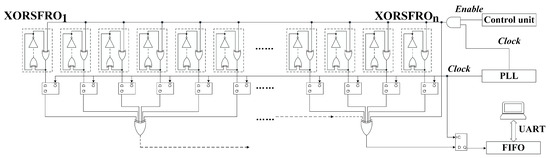
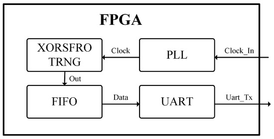
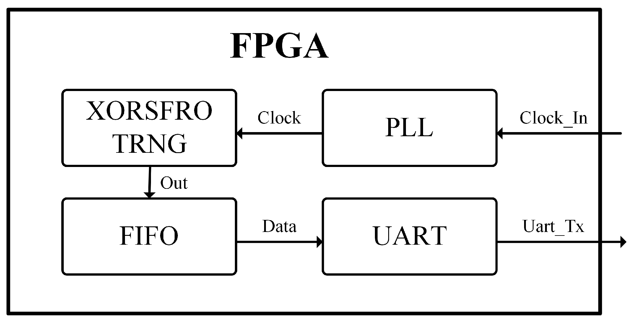
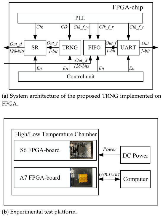
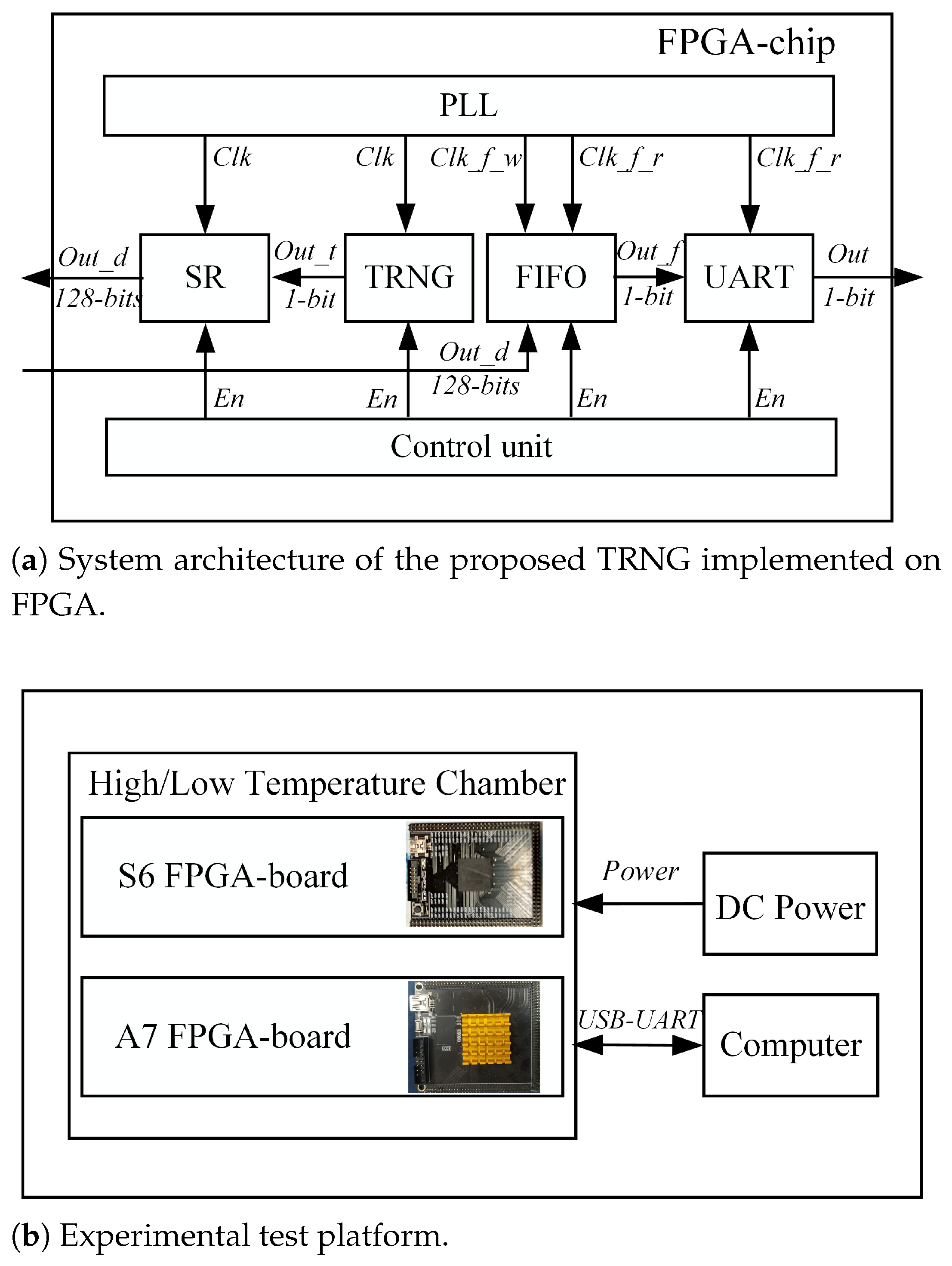
To validate the proposed XORSFRO TRNG, we implemented and evaluated it on off-the-shelf FPGA platforms. The verification system is composed of 10 parallel 11-stage XORSFRO units. To mitigate board-specific randomness, two Xilinx Spartan-6 XC6SLX16 FPGA boards (45 nm process) and two Xilinx Artix-7 XC7A35T FPGA boards (28 nm process) were selected as target devices for implementation. The development toolchains used were Xilinx ISE 14.7 and Vivado 2018.3. Standard operating conditions were set at 25 °C with supply voltages of 1.2 V for Spartan-6 and 1.0 V for Artix-7, respectively. Figure 7 presents the complete block diagram of the experimental platform. An external crystal oscillator provides a 50 MHz clock signal, which is multiplied via a PLL to generate a 400 MHz clock for Spartan-6 and a 500 MHz clock for Artix-7. Since one bit is generated in every PLL cycle, the throughput of each XORSFRO unit is equal to the respective PLL frequency. The TRNG output is first buffered through a 1024-bit First-In First-Out (FIFO) and then transmitted to a host computer via USB-UART, where post-processing operations are performed on the received data.
Figure 7.
XORSFRO TRNG test architecture.
As shown in Figure 8, the proposed TRNG is implemented on the FPGA platform with a control unit, shift register (SR), FIFO, and Universal Asynchronous Receiver-Transmitter (UART) interface. The design enables real-time data collection and communication while maintaining compact hardware overhead.
Figure 8.
Overall FPGA implementation of the proposed TRNG.
In this work, five evaluation metrics were employed to assess the performance of the XORSFRO TRNG: the NIST tests (including both NIST SP 800-22 and NIST SP 800-90B), the Deviation Test, the Autocorrelation Test, the Restart Test, and the PVT Test. Finally, the proposed XORSFRO TRNG is compared with recent FPGA-based state-of-the-art TRNG architectures in terms of performance and resource utilization, from which the conclusions are drawn.
4.1. NIST Test
In this subsection, the performance of the XORSFRO TRNG is evaluated using the NIST SP 800-22 and NIST SP 800-90B test suites.
NIST SP 800-22 consists of 15 statistical tests, each producing a P-value that reflects the likelihood that the tested sequence is truly random. A sequence is considered to pass a test when its P-value is greater than 0.01, and the overall proportion of passing sequences should ideally be close to 1. For each FPGA board, ten datasets were collected, each containing one million output bits generated under nominal operating conditions. The results, summarized in Table 2, show that the generated sequences consistently achieved p-values above 0.01, with average pass rates exceeding 96%. Slight variations in p-values are attributed to chip-to-chip process variations rather than deficiencies in the TRNG design.
Table 2.
NIST SP 800-22 test results on different FPGA families.
NIST SP 800-90B further evaluates entropy quality by estimating the minimum entropy (h-min) of the output bitstream using non-IID (non-independent and identically distributed) tests. This standard reports maximum probability(p-max), the maximum probability of observing the most frequent symbol, and derives h-min as the worst-case entropy per bit. For each FPGA device, one million output bits were analyzed. From Table 3, it can be seen that the minimum entropy values of the proposed TRNG are 0.899598 and 0.903432 on Spartan-6, and 0.936991 and 0.911052 on Artix-7, confirming that the design maintains strong unpredictability across different FPGA platforms.
Table 3.
Different FPGA series NIST SP 800-90B entropy analysis results.
Together, these results demonstrate that the proposed XORSFRO successfully passes both NIST SP 800-22 and SP 800-90B suites without requiring post-processing, validating its ability to generate high-quality random sequences suitable for cryptographic applications in distributed PV systems.
4.2. Deviation Test
While statistical test suites validate the overall randomness properties of generated sequences, they do not directly reflect the bit-level uniformity of the TRNG output. To further evaluate distribution balance, we performed a Deviation Test, which measures the deviation rate between the number of ‘1’s and ‘0’s in the output sequence. Ideally, in a continuous random sequence, the probabilities of generating ‘0’ and ‘1’ should both be 50% [20]. However, in practice, the output of a TRNG may exhibit bias due to the influence of factors such as voltage, temperature, and noise. If the generated sequence shows excessive bias, it may be susceptible to adversarial attacks.
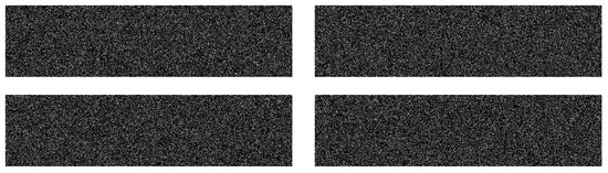
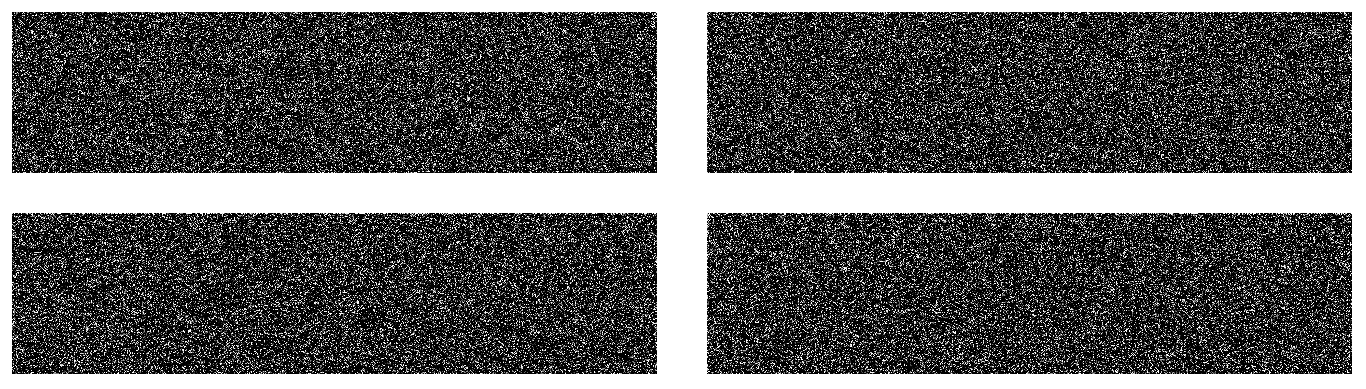
In this subsection, one million consecutive bits were generated on the FPGA boards under test under standard operating conditions, and the collected data were visualized as bitstream images. Figure 9 illustrates the generated bitstream images, where black pixels represent ‘1’ and white pixels represent ‘0’. It can be observed that the distribution of black and white pixels is uniform, indicating that the number of ‘0’s and ‘1’s in the generated random sequences is approximately equal. Furthermore, the statistical bias of the proposed TRNG on different FPGA boards can be calculated using Equation (6).
Figure 9.
Deviation test result bitstream images of Spartan-6 FPGAs and Artix-7 FPGAs.
In Equation (14), and denote the numbers of ‘0’s and ‘1’s in the random sequence, respectively.
As shown in Table 4, the statistical bias of the TRNG random sequences generated on the four tested FPGA boards is presented. This demonstrates that the proposed TRNG is capable of generating random sequences with low bias.
Table 4.
Bias test results of Spartan-6 FPGAs and Artix-7 FPGAs.
4.3. Autocorrelation Test
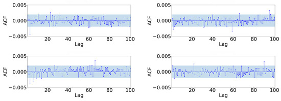
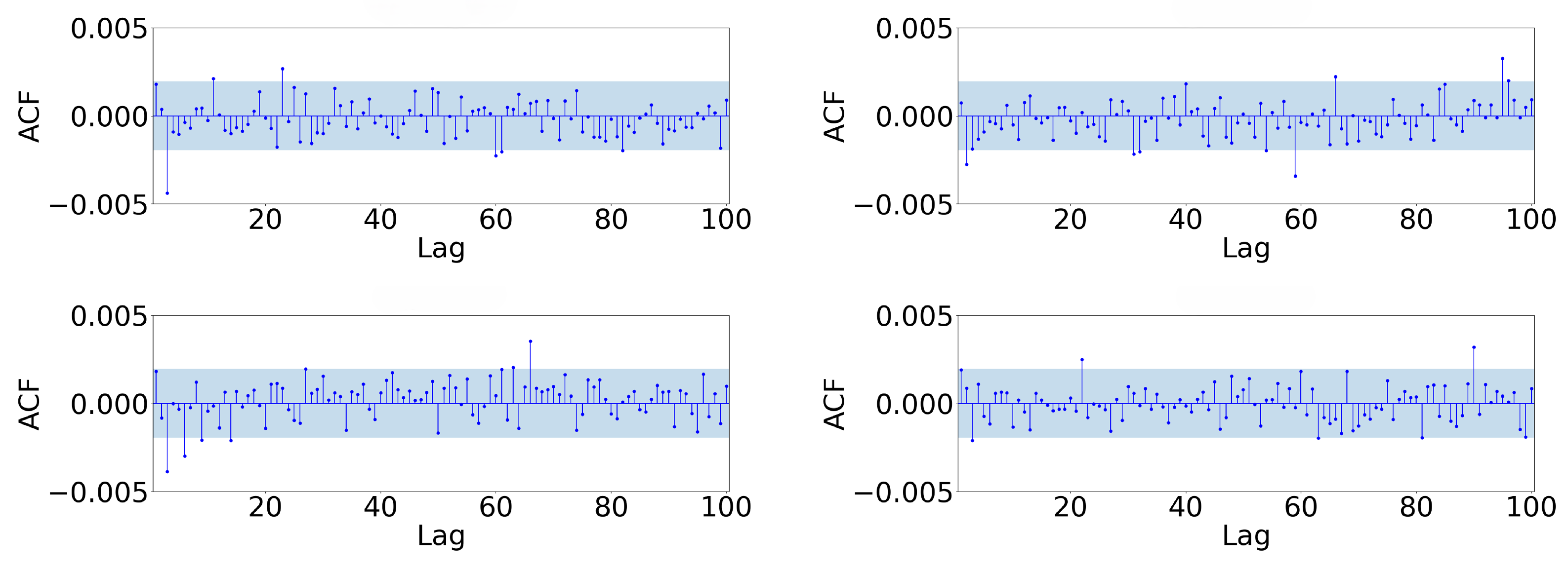
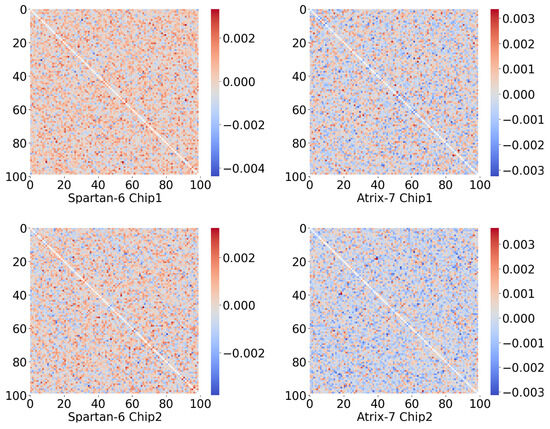
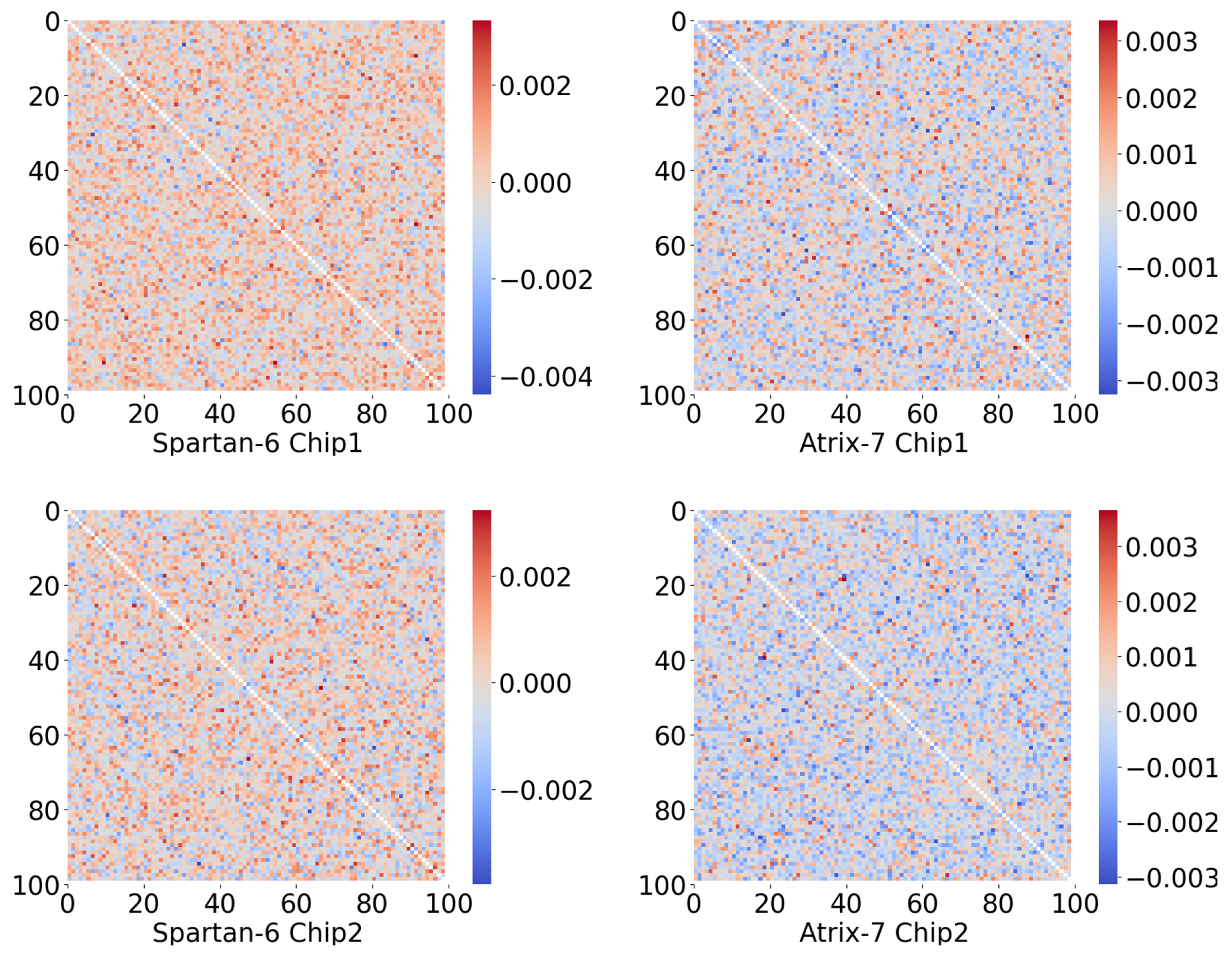
Ideally, the bits generated by a TRNG at different time instances should be uncorrelated. The correlation between different time instances in a random sequence can be evaluated using the autocorrelation coefficient. In our experiments, one million consecutive bits were collected from both Spartan-6 and Artix-7 FPGA boards, and the autocorrelation coefficients were computed using Python 3.10. The lag values in the autocorrelation function were set from 1 to 100, and the autocorrelation factors (ACF) between variables with lags of 1 to 100 bits were analyzed. According to the statistical index designed by Karl Pearson, a correlation coefficient below 0.3 can be regarded as uncorrelated.
The results of the autocorrelation test are shown in Figure 10, where the ACF values of all datasets fluctuate within , indicating that all correlation coefficients are well below 0.3. Therefore, it can be concluded that the random sequences generated by the proposed TRNG exhibit no autocorrelation.
Figure 10.
Autocorrelation test results on Spartan-6 FPGAs and Artix-7 FPGAs.
4.4. Restart Test
Ideally, the random sequences generated by a TRNG should be different each time it is powered on. Therefore, in this subsection, six sets of 30 consecutive bits were collected under standard operating conditions from both Spartan-6 and Artix-7 FPGA boards. As shown in Figure 11, all the random sequences are distinct, indicating that the TRNG generates different random bitstreams after each power-up. Hence, it can be concluded that the random sequences produced by the TRNG exhibit no similarity and possess strong randomness.
Figure 11.
The results of restart test.
4.5. PVT Test
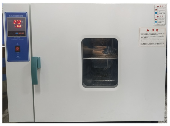
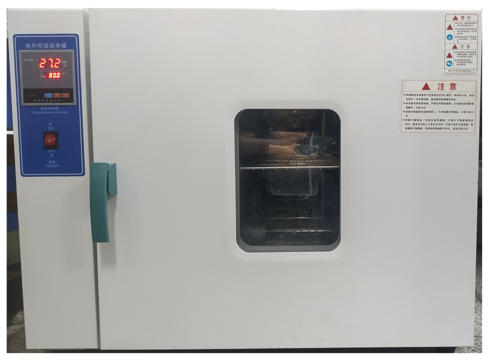
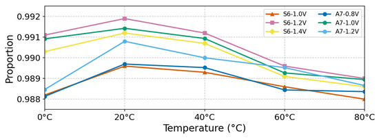
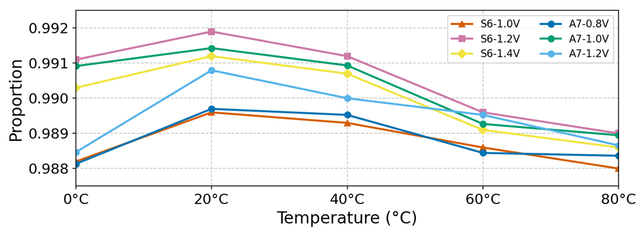
The output quality of a TRNG can be affected by factors such as voltage, temperature, and noise. Therefore, we evaluated the performance of the XORSFRO under different temperature and voltage conditions, as illustrated in Figure 12. A DC power supply and a computer interface were used to provide stable operation and data acquisition. Standard operating conditions were defined as follows: 20 °C and 1.2 V for Spartan-6, and 20 °C and 1.0 V for Artix-7. The temperature was varied from 0 °C to 80 °C in steps of 20 °C, while the voltage ranged from 1.0 V to 1.4 V for Spartan-6 and from 0.8 V to 1.2 V for Artix-7. For each step, ten sets of random bitstreams, each containing one million bits, were collected. The NIST SP 800-22 test suite was then used to evaluate the percentage of tests passed (hereafter referred to as the pass rate). The results are illustrated in Figure 12.
Figure 12.
PVT test environment.
From Figure 13, it can be observed that, for both Spartan-6 and Artix-7, the highest pass rates were achieved at temperatures between 0 °C and 20 °C under the nominal supply voltage, indicating the best randomness in this range. However, as the temperature increases, the pass rate of the XORSFRO decreases across different FPGA boards. In addition, variations in voltage also influence the pass rate. At lower voltages, the generated bitstreams exhibit reduced pass rates, with a more rapid decline as the temperature increases. Although the decrease in pass rate is less pronounced at higher voltages compared to lower voltages, neither condition is as stable as the nominal voltage.
Figure 13.
Results of PVT test on Spartan-6 and Artix-7 FPGAs.
4.6. Comparison with Other TRNGs Based on FPGAs
In this subsection, we compare the performance of the proposed XORSFRO TRNG with state-of-the-art TRNGs across seven dimensions (from the third to the ninth columns of Table 4): (1) TRNG implementation platform; (2) chip technology node; (3) ES circuit of the TRNG; (4) hardware cost (including LUTs, DFFs, and CARRY4s); (5) TRNG throughput (Mbps); (6) throughput-to-slice ratio (Mbps/Slice); and (7) TRNG runtime power consumption. The comparison results are presented in Table 5.
Table 5.
Comparison of FPGA-based TRNG implementations.
From Table 5, it can be observed that all of these TRNGs are implemented on advanced FPGA platforms and most exhibit strong performance. Wu et al. [29] achieved a throughput of 150 Mbps, but with a resource cost of 298 LUTs. Della et al. [23] implemented a design with only 4 LUTs and 3 DFFs, but the throughput was limited to 0.76 Mbps. Frustaci et al. [11] achieved higher throughput, yet their throughput-to-slice ratio still requires improvement. In addition, the TRNGs proposed by Wang et al. [20] and Lin et al. [24]. also require better resource utilization.
In contrast, the proposed XORSFRO TRNG achieves throughputs of 400 Mbps (S6) and 500 Mbps (A7) while using 32 LUTs and 11 DFFs, resulting in throughput-to-slice ratios of 66.7 and 83.3. These values are 8.45× and 10.56× higher, respectively, than those reported in [11]. This demonstrates that our method achieves low hardware cost and high throughput, making it highly suitable for resource-constrained devices.
5. Conclusions
In this work, we proposed a high-entropy TRNG based on a high-speed feedback structure, where the random output is fed back to alter the oscillation state of FXOR-ROs and amplify jitter. Experimental results on Xilinx Spartan-6 and Artix-7 FPGAs show that the proposed TRNG requires 32 LUTs and 11 DFFs while achieving throughputs of 400 Mbps and 500 Mbps. Compared with existing FPGA-based TRNGs, our design is more compact, consumes significantly fewer resources, and achieves ultra-high throughput. Moreover, the new RO structure demonstrates strong potential for enhancing TRNG performance, making it a promising solution for generating high-quality and efficient random data.
Author Contributions
Conceptualization, J.W.; methodology, W.G.; software, W.G. and R.X.; validation, J.W., B.D. and C.X.; formal analysis, Y.Z.; investigation, W.G. and J.L.; data curation, Y.Z. and J.L.; writing—original draft preparation, W.G. and J.L.; writing—review and editing, Y.Z. and J.L.; supervision, J.W.; project administration, Y.Z.; funding acquisition, W.G. All authors have read and agreed to the published version of the manuscript.
Funding
This research was funded by the Science and Technology Project of China Huaneng Group Corporation under grant number HNKJ23-HF64, and the National Natural Science Foundation of China under grant number 62167009.
Data Availability Statement
The original contributions presented in this study are included in the article. Further inquiries can be directed to the corresponding authors.
Acknowledgments
The authors would like to thank Junjun Wang and Zhao Huang, as well as the editors and reviewers for their efforts and suggestions to improve our manuscript.
Conflicts of Interest
Authors Wei Guo and Jingcheng Wang were employed by the company Xi’an Thermal Power Research Institute Co., Ltd. Authors Rui Xia, Bosong Ding, and Chao Xiong were employed by the company Huaneng Power International Co., Ltd. Anhui Wind Power Branch. The remaining authors declare that the research was conducted in the absence of any commercial or financial relationships that could be construed as a potential conflict of interest. The authors declare that this study was funded by the Science and Technology Project of China Huaneng Group Corporation. The funder was not involved in the study design, collection, analysis, interpretation of data, the writing of this article, or the decision to submit it for publication.
Abbreviations
| TRNG | True Random Number Generator |
| ES | Entropy Source |
| PV | Photovoltaic |
| IoT | Internet of Things |
| RO | Ring Oscillator |
| STR | Self-Timed Ring |
| DCM | Digital Clock Manager |
| PLL | Phase-Locked Loop |
| PVT | Process–Voltage–Temperature |
| FPGA | Field-Programmable Gate Array |
| XOR | Exclusive OR |
| XNOR | Exclusive NOR |
| XORSFRO | XOR Self-Feedback Ring Oscillator |
| DFF | D-type Flip-Flop |
| SR | Shift Register |
| FIFO | First-In First-Out |
| UART | Universal Asynchronous Receiver-Transmitter |
| Clk | System Clock |
| ACF | Autocorrelation factor |
| LUT | Look-Up Table |
| MCV | Most Common Value |
| h-min | Minimum Entropy |
| p-max | Maximum Probability |
| NAND | NOT AND Gate |
| NOR | NOT OR Gate |
References
- Harrou, F.; Taghezouit, B.; Bouyeddou, B.; Sun, Y. Cybersecurity of Photovoltaic Systems: Challenges, Threats, and Mitigation Strategies: A Short Survey. Electronics 2023, 12, 1274451. [Google Scholar] [CrossRef] [Scilit]
- Orúe López, A.B.; Encinas, L.H.; Muñoz, A.M.; Vitini, F.M. A lightweight pseudorandom number generator for securing the Internet of Things. IEEE Access 2017, 5, 27800–27806. [Google Scholar] [CrossRef] [Scilit]
- Serrano, R.; Duran, C.; Sarmiento, M.; Hoang, T.-T.; Tsukamoto, A.; Suzaki, K.; Pham, C.-K. A robust and healthy against PVT variations TRNG based on frequency collapse. IEEE Access 2022, 10, 41852–41862. [Google Scholar] [CrossRef] [Scilit]
- Koyuncu, İ.; Tuna, M.; Pehlivan, İ.; Fidan, C.B.; Alçin, M. Design, FPGA implementation and statistical analysis of chaos-ring based dual entropy core true random number generator. Analog Integr. Circuits Signal Process. 2020, 102, 445–456. [Google Scholar] [CrossRef] [Scilit]
- IEA-PVPS. Trends in Photovoltaic Applications 2024. International Energy Agency Photovoltaic Power Systems Programme. 2024. Available online: https://iea-pvps.org/wp-content/uploads/2024/10/IEA-PVPS-Task-1-Trends-Report-2024.pdf (accessed on 15 September 2025).
- Choe, J.-Y.; Shin, K.-W. A self-timed ring based TRNG with feedback structure. In Proceedings of the 2020 International Conference on Electronics, Information, and Communication (ICEIC), Barcelona, Spain, 19–22 January 2020; pp. 1–3. [Google Scholar]
- Gu, H.; Deng, F.; Wang, Q.; Jing, N. A four-phase self-timed ring based true random number generator on FPGA. In Proceedings of the 2022 IEEE 16th International Conference on Solid-State & Integrated Circuit Technology (ICSICT), Nanjing, China, 25–28 October 2022; pp. 1–3. [Google Scholar]
- Fujieda, N.; Takeda, M.; Ichikawa, S. An analysis of DCM-based true random number generator. IEEE Trans. Circuits Syst. II Express Briefs 2020, 67, 1109–1113. [Google Scholar] [CrossRef] [Scilit]
- Riurean, S.; Fodorean, D.; Rusu, M.C.; Drosu, A.L. Securing photovoltaic systems as critical infrastructure. Sustainability 2025, 17, 4397. [Google Scholar] [CrossRef] [Scilit]
- Johnson, A.P.; Chakraborty, R.S.; Mukhopadyay, D. An improved DCM-based tunable true random number generator for Xilinx FPGA. IEEE Trans. Circuits Syst. II Express Briefs 2017, 64, 452–456. [Google Scholar] [CrossRef] [Scilit]
- Frustaci, F.; Spagnolo, F.; Perri, S.; Corsonello, P. A high-speed FPGA-based true random number generator using metastability with clock managers. IEEE Trans. Circuits Syst. II Express Briefs 2023, 70, 756–760. [Google Scholar] [CrossRef] [Scilit]
- Maiti, A.; Schaumont, P. Improved Ring Oscillator PUF: An FPGA-friendly Secure Primitive. J. Cryptol. 2011, 24, 375–397. [Google Scholar] [CrossRef] [Scilit]
- Mei, F.; Zhang, L.; Gu, C.; Cao, Y.; Wang, C.; Liu, W. A highly flexible lightweight and high speed true random number generator on FPGA. In Proceedings of the 2018 IEEE Computer Society Annual Symposium on VLSI (ISVLSI), Hong Kong, China, 8–11 July 2018; pp. 399–404. [Google Scholar]
- Sivaraman, R.; Arumugham, S.; Rajagopalan, S. Design and analysis of ring oscillator influenced beat frequency detection for true random number generation on FPGA. In Proceedings of the 2019 11th International Conference on Computing, Communication and Networking Technologies (ICCCNT), Coimbatore, India, 7–11 January 2019; pp. 1–6. [Google Scholar]
- Xu, X.; Liang, H.; Zhou, K.; Ma, G.; Huang, Z.; Yi, M.; Ni, T.; Lu, Y. An all-digital and jitter-quantizing true random number generator in SRAM-based FPGAs. In Proceedings of the 2018 IEEE Asian Test Symposium (ATS), Hefei, China, 15–18 October 2018; pp. 59–62. [Google Scholar]
- Lu, Z.; Qidiao, H.; Chen, Q.; Liu, Z.; Zhang, J. An FPGA-compatible TRNG with ultra-high throughput and energy efficiency. In Proceedings of the 2023 60th ACM/IEEE Design Automation Conference (DAC), San Francisco, CA, USA, 9–13 July 2023; pp. 1–6. [Google Scholar] [CrossRef] [Scilit]
- Tao, S.; Yu, Y.; Dubrova, E. FPGA-based true random number generators using non-linear feedback ring oscillators. In Proceedings of the 2018 16th IEEE International New Circuits and Systems Conference (NEWCAS), Montreal, QC, Canada, 24–27 June 2018; pp. 213–216. [Google Scholar]
- Cui, J.; Yi, M.; Cao, D.; Yao, L.; Wang, X.; Liang, H.; Huang, Z.; Qi, H.; Ni, T.; Lu, Y. Design of true random number generator based on multi-stage feedback ring oscillator. IEEE Trans. Circuits Syst. II Express Briefs 2022, 69, 1752–1756. [Google Scholar] [CrossRef] [Scilit]
- Peng, Q.; Bian, J.; Huang, Z.; Wang, S.; Yan, A. A compact TRNG design for FPGA based on the metastability of RO-driven shift registers. ACM Trans. Des. Autom. Electron. Syst. 2023, 29, 1–17. [Google Scholar] [CrossRef] [Scilit]
- Wang, X.; Liang, H.; Wang, Y.; Yao, L.; Guo, Y.; Yi, M.; Huang, Z.; Qi, H.; Lu, Y. High-throughput portable true random number generator based on jitter-latch structure. IEEE Trans. Circuits Syst. I Reg. Papers 2021, 68, 741–753. [Google Scholar] [CrossRef] [Scilit]
- Grujić, M.; Verbauwhede, I. TROT: A three-edge ring oscillator based true random number generator with time-to-digital conversion. IEEE Trans. Circuits Syst. I Reg. Papers 2022, 69, 2435–2448. [Google Scholar] [CrossRef] [Scilit]
- Yang, Y.; Jia, S.; Wang, Y.; Zhang, S.; Liu, C. A reliable true random number generator based on novel chaotic ring oscillator. In Proceedings of the 2017 IEEE International Symposium on Circuits and Systems (ISCAS), Baltimore, MD, USA, 28–31 May 2017; pp. 1–4. [Google Scholar]
- Della Sala, R.; Bellizia, D.; Scotti, G. A novel ultra-compact FPGA-compatible TRNG architecture exploiting latched ring oscillators. IEEE Trans. Circuits Syst. II Express Briefs 2022, 69, 1672–1676. [Google Scholar] [CrossRef] [Scilit]
- Lin, J.; Wang, Y.; Zhao, Z.; Hui, C.; Song, Z. A new method of true random number generation based on Galois ring oscillator with event sampling architecture in FPGA. In Proceedings of the IEEE International Instrumentation and Measurement Technology Conference (I2MTC), Dubrovnik, Croatia, 25–28 May 2020; pp. 1–5. [Google Scholar]
- Della Sala, R.; Scotti, G. On enhancing the throughput of the latched ring oscillator TRNG on FPGA. In Proceedings of the International Conference on Applications in Electronics Pervading Industry, Environment and Society, Genova, Italy, 26–27 September 2023; pp. 277–287. [Google Scholar] [CrossRef] [Scilit]
- Zhang, Y.; Zhang, J. A high throughput STR-based TRNG by jitter precise quantization superposing. ACM Trans. Des. Autom. Electron. Syst. 2023, 29, 1–19. [Google Scholar] [CrossRef] [Scilit]
- Tupparwar, S.; Mohankumar, N. A hybrid true random number generator using ring oscillator and digital clock manager. In Proceedings of the 6th International Conference on Inventive Computation Technologies (ICICT), Coimbatore, India, 20–22 January 2021; pp. 290–294. [Google Scholar]
- Sivaraman, R.; Rajagopalan, S.; Sridevi, A.; Rayappan, J.B.B.; Annamalai, M.P.V.; Rengarajan, A. Metastability-induced TRNG architecture on FPGA. Iran. J. Sci. Technol. Trans. Electr. Eng. 2019, 44, 47–57. [Google Scholar] [CrossRef] [Scilit]
- Wu, X.; Li, S. A new digital true random number generator based on delay chain feedback loop. In Proceedings of the IEEE International Symposium on Circuits and Systems (ISCAS), Baltimore, MD, USA, 28–31 May 2017; pp. 1–4. [Google Scholar]



Disclaimer/Publisher’s Note: The statements, opinions and data contained in all publications are solely those of the individual author(s) and contributor(s) and not of MDPI and/or the editor(s). MDPI and/or the editor(s) disclaim responsibility for any injury to people or property resulting from any ideas, methods, instructions or products referred to in the content. |
© 2025 by the authors. Licensee MDPI, Basel, Switzerland. This article is an open access article distributed under the terms and conditions of the Creative Commons Attribution (CC BY) license.