1. Introduction
MMC has become a key technology for high-voltage and high-power applications due to their modularity, scalability, and high-quality output waveforms. They are widely used in HVDC transmission, medium-voltage distribution networks, and flexible AC transmission systems. The modular architecture allows low-voltage power devices to share voltage, simplifying design and enhancing reliability.
Recently, the integration of energy storage into MMCs has attracted significant attention, leading to the development of ES-MMCs. Unlike conventional MMCs, ES-MMCs incorporate batteries, supercapacitors, or hybrid storage devices directly within submodules. This enables each submodule to function as both a power conversion stage and an independent energy storage unit, enhancing system flexibility and enabling bidirectional power exchange with the AC grid and DC link. ES-MMCs support grid stability, frequency regulation, peak shaving, fault tolerance, and operation under weak grid or islanded conditions, making them particularly suitable for renewable energy integration and hybrid power management.
However, energy storage integration introduces new challenges. Distributed storage alters internal power flow, often causing imbalances between upper and lower arm voltages and unequal energy utilization among phases [
1,
2,
3,
4]. Traditional voltage-balancing methods for non-storage MMCs are insufficient for ES-MMCs, especially under dynamic power exchange conditions.
Several methods have been proposed to address these issues. In [
5], differential-mode fundamental-frequency components are added to the modulation voltages of the upper and lower arms, effectively regulating interphase and arm voltage differences, though this may introduce harmonic currents on the AC side. References [
1,
2,
3,
4,
6,
7] control the positive- and negative-sequence amplitudes of fundamental-frequency common-mode currents to balance capacitor voltages between phases and arms. However, under light-load or no-load conditions, the absence of DC in the arms eliminates the power path for phase capacitor balancing, leaving intra-arm capacitor voltages unregulated [
5]. Asymmetric power distribution strategies [
8] adjust output power for each phase and arm, enabling coordinated voltage balancing, but practical implementation remains complex. A generalized voltage balancing algorithm based on dynamic switching state selection is proposed, in which the switching states of the submodules are generated dynamically [
9,
10]. Ref. [
11] analyzed the causes of capacitor voltage imbalance and proposed a control strategy based on fundamental-frequency reactive circulating current injection. Ref. [
12] achieved submodule capacitor voltage balancing by introducing a regulation coefficient into the modulation. Refs. [
13,
14,
15,
16,
17,
18,
19,
20,
21,
22,
23,
24] also investigated the principles of capacitor voltage behavior and balancing control methods related to CPS-PWM, providing the theoretical foundation for this paper.
This paper proposes a self-synchronized common-mode current strategy for power rebalancing in ES-MMCs, with 2 main contributions:
Regulation of upper and lower arm capacitor voltages through control of the phase angle between the modulation voltage and the fundamental-frequency common-mode current, while maintaining phase capacitor voltage stability via a DC common-mode offset.
Establishment of a dedicated and controllable power-balancing pathway by maintaining a constant common-mode current amplitude, which enhances capacitor voltage balancing, operational stability, and enables flexible energy management under varying load and grid conditions.
3. Self-Synchronized Common-Mode Strategy
3.1. Capacitor Voltage Balancing Principle of Common-Mode Current
As shown in (9), to achieve both the average capacitor voltage regulation across all submodules in phase
j and the voltage balance between the upper and lower arms, a DC common-mode component
(
t) and a fundamental-frequency common-mode component
(
t) are introduced into the modulation voltages of the upper and lower arms
(
t) and
(
t). The output voltage (or modulation voltage) of the upper arm can be expressed as
The fundamental-frequency common-mode voltage component in phase
j is defined as
where
denotes the amplitude of the fundamental-frequency common-mode voltage, and
represents its phase angle relative to the reference differential-mode voltage
(
t).
Accordingly, in (10), the upper- and lower-arm currents
(
t) and
(
t) are augmented compared with (4) by the introduction of the fundamental-frequency common-mode current component:
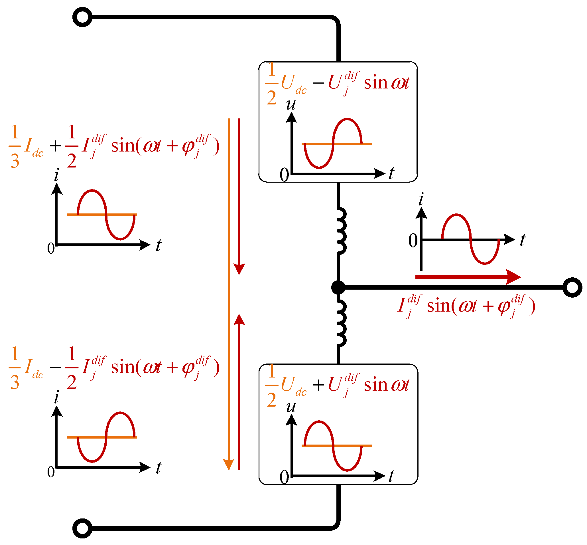
The instantaneous powers of the upper and lower arms, denoted as
(
t) and
(
t), are illustrated in
Figure 5 and
Figure 6, respectively.
Figure 5 depicts the decomposition of the upper-arm power into its DC, differential-mode, and common-mode components, while
Figure 6 presents the corresponding decomposition for the lower arm.
In
Figure 5 and
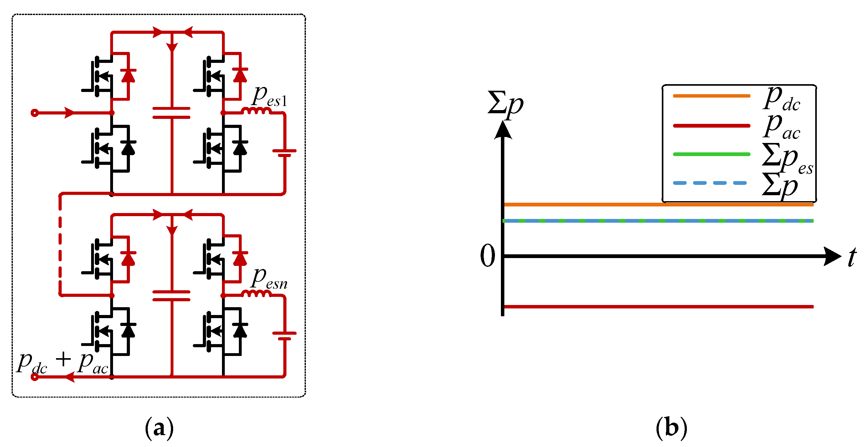
Figure 6, the product and superposition of the voltage and current components yield relatively complex expressions for instantaneous power. However, rather than focusing on the instantaneous power fluctuations, the primary concern lies in the periodic variations in the capacitor power in the upper and lower arms, namely the DC component of the power. Therefore, a moving average filter with a 0.02-s (50 Hz) time constant is applied to the output power to extract its DC component.
Then, by applying the moving average filter with an averaging interval of Ts, the DC components of the instantaneous powers in the upper and lower arms can be obtained as (12).
The DC components of the arm powers can be further decomposed into common-mode and differential-mode parts in (11). Specifically, the averaged common-mode and differential-mode power components over the window
Ts are defined as
By regulating <(t)>Ts, the phase input power can be adjusted; in other words, the common-mode component of the DC power can be used to control the average capacitor voltage of the phase. Similarly, by controlling <(t)>Ts, the differential power between the upper and lower arms can be modulated, allowing the differential DC component to be regulated and thereby achieving voltage balance between the upper and lower arm capacitors.
In <(t)>Ts, the power exchange process between the DC and AC sides is not affected by the common-mode voltage component. Among the remaining three terms, the dominant contribution arises from the DC component of , which is used to regulate the average capacitor voltage of phase j. Furthermore, this DC component of the common-mode current can be realized by controlling the DC component of the common-mode modulation voltage, (t), applied to the arm output voltage.
In <
(
t)>
Ts, the differential-mode voltage
is typically much larger than the common-mode voltage
, making it the dominant term. The power balance between the upper and lower arms can be regulated by controlling either the amplitude of the common-mode current
or the phase angle
between the common-mode current
(
t) and the differential-mode voltage
(
t). As reported in [
1,
2,
4,
5], maintaining
= 0 and adjusting the amplitude of the common-mode modulation voltage
(
t) allows regulation of
(
t), thereby achieving voltage balance between the upper- and lower-arm capacitors.
However, amplitude-based control has a drawback under low-power operation on the AC/DC side of the MMC. Due to small power fluctuations, the resulting common-mode current is also small, and the current flowing through the arms is insufficient to redistribute power among the submodules within the arms. Consequently, although the upper- and lower-arm capacitor voltages may remain balanced, the capacitor voltages within the same arm can become unbalanced if the output powers of the submodule storage units are asymmetric.
Therefore, in this study, the arm voltage balance is achieved by regulating the phase angle . However, when ≠ 0, the presence of the common-mode current induces fundamental-frequency reactive power exchange between the upper and lower arms. Direct control under these conditions would require frequent adjustments of the phase angle, which can degrade both control stability and performance. To mitigate this issue, a fundamental-frequency moving-average filter is applied to extract the DC component of the arm capacitor power for control, thereby avoiding the influence of reactive power. Furthermore, by superimposing a DC common-mode voltage (t) on the fundamental-frequency common-mode voltage (t), regulation of the average capacitor voltage of the phase is achieved.
This decomposition and control strategy thus establish a phase-level power transfer channel within each arm and provide an effective mechanism for capacitor power rebalancing, particularly under persistent asymmetry conditions introduced by distributed energy storage units.
3.2. Modeling and Synchronization Mechanism of Common-Mode Power
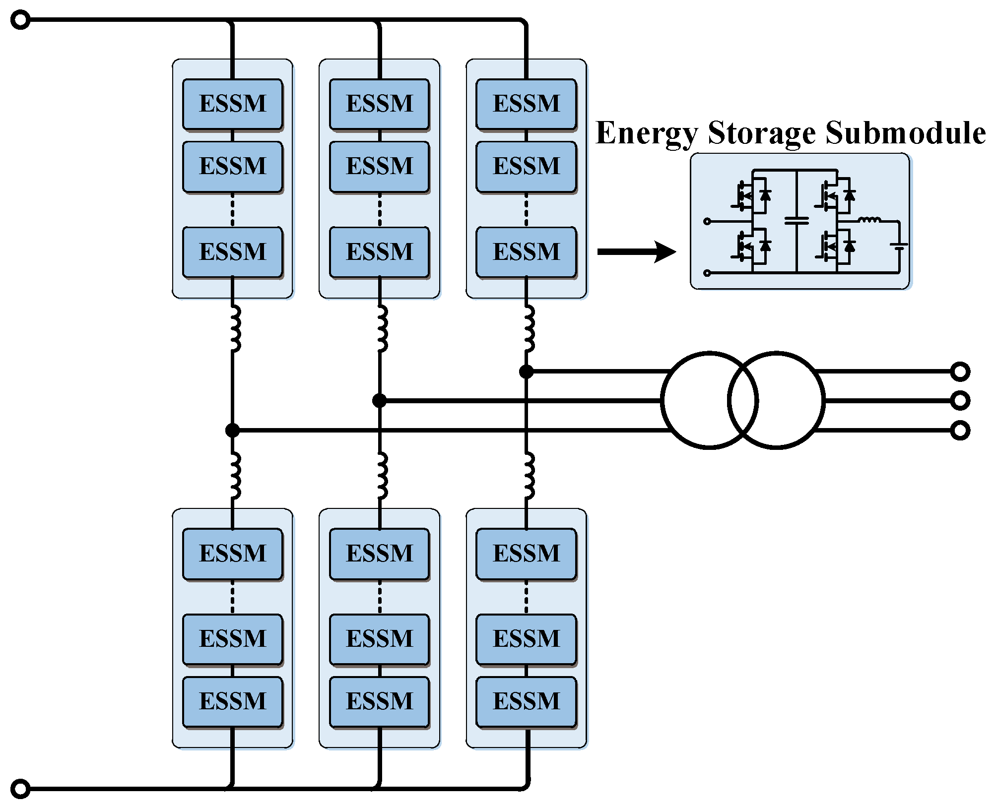
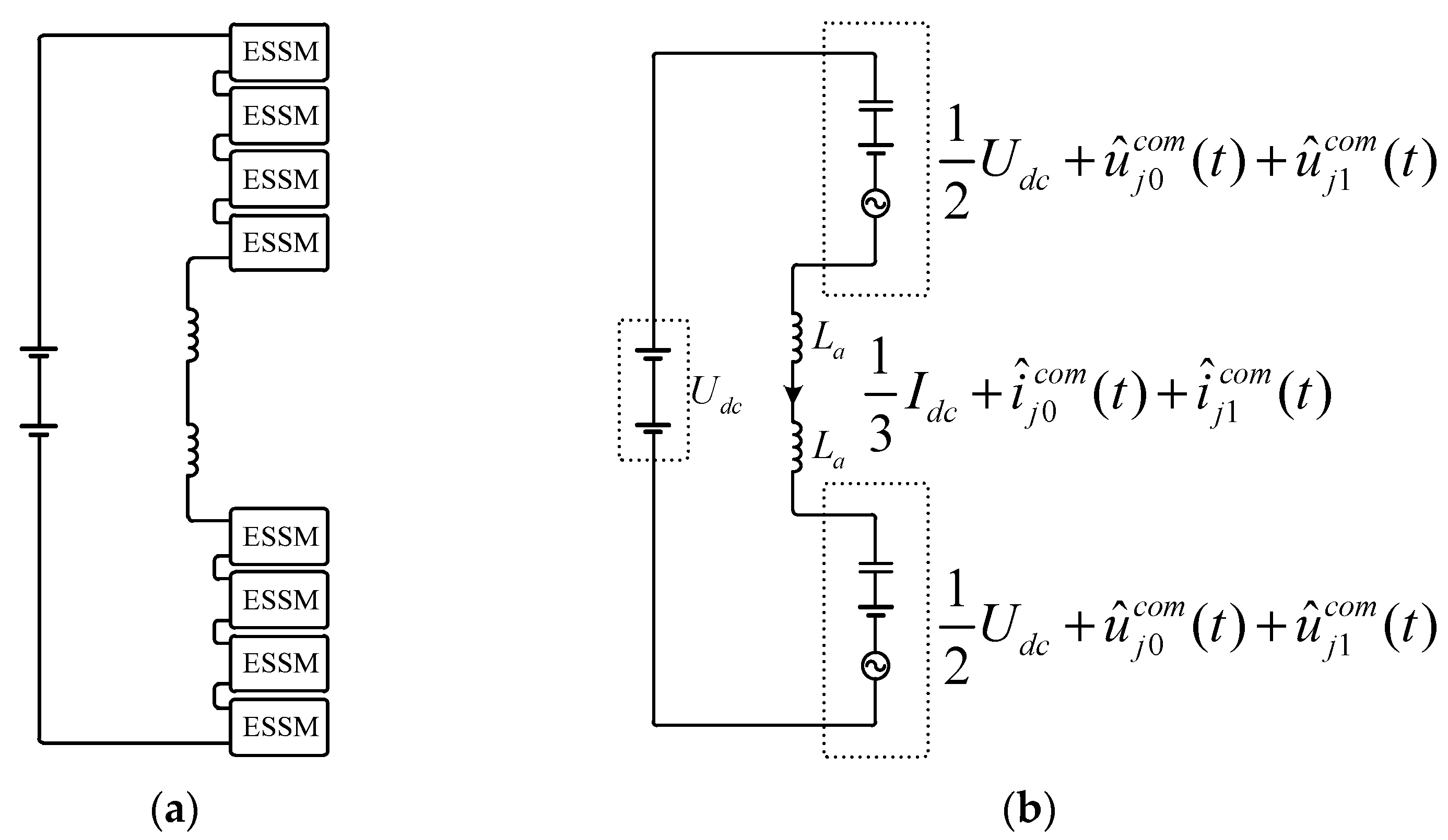
Figure 7a illustrates the phase topology of the ES-MMC, which consists of upper-arm submodules, lower-arm submodules, and arm inductors. Compared with the DC component of the arm
and the differential-mode voltage
(
t), both the superimposed DC common-mode voltage and the fundamental-frequency common-mode voltage can be considered as small-signal perturbations, as shown in
Figure 7b.
The DC common-mode voltage component (t) is denoted as , and the fundamental-frequency common-mode voltage component (t) is denoted as . These small-signal components are simultaneously superimposed onto the modulation signals of the upper and lower arms, generating corresponding small-signal common-mode currents in the arms, consisting of a DC component and a fundamental-frequency component .
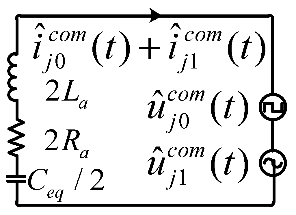
Figure 8 illustrates the small-signal circuit model derived from
Figure 7 by separating the steady-state point. In this equivalent model, the arm inductance
La and its internal resistance
Ra are represented,
Ceq is the equivalent capacitor from the submodule after modulation, across which a controlled DC voltage and a sinusoidal voltage are applied. Consequently, the process of generating the common-mode DC and the common-mode fundamental current can be effectively described.
Figure 8 demonstrates that the amplitude of the output currents
and
can be regulated by adjusting the amplitudes of the DC and fundamental-frequency common-mode voltages. Moreover, by controlling the phase angle
of the fundamental-frequency common-mode voltage, the synchronization angle
of the common-mode current can be effectively modulated.
The periodic discrete control waveform of the common-mode current
is illustrated in
Figure 9. To ensure the integrity of the synchronization-angle control process, the control angle
(
t) within the common-mode voltage is updated only at the end of each fundamental cycle. Accordingly, the proposed synchronization-angle control strategy adopts a discrete control scheme with a period of 0.02 s. At the beginning of each cycle, the small-signal component derived from the sum of the phase capacitor voltages
is employed to adjust the amplitude. In contrast, the small-signal component
obtained from the difference between the upper- and lower-arm voltages is used to regulate
(
t), thereby controlling the angle
(
t).
The phase relationship among the fundamental common-mode voltage control angle
(
t), the synchronization angle of the fundamental common-mode current
(
t), and the differential voltage
(
t) is illustrated in
Figure 10. By taking the differential voltage
(
t) as the reference phase, denoted as the d-axis, the control angle
(
t) is defined as a small-signal deviation relative to this reference. Due to the presence of the arm inductance, the inductor current lags behind the reference by
(
t). Its steady-state point is aligned with the q-axis, and the deviation of the synchronization angle relative to this steady-state point is denoted as a small-signal perturbation
.
The fundamental common-mode current vector can be projected onto the upper- and lower-arm differential voltages and as cos, which corresponds to the active power exchanged between the two arms. From the vector diagram, it is evident that, under the influence of the fundamental common-mode current, the power output directions of the upper and lower arms are always opposite. This observation is consistent with the analytical results presented in Equation (13).
The control angle
(
t) operates within a regulation interval centered on the d-axis, [−0.5π, 0.5π]. This interval can be further divided into six regions (I–VI), as illustrated in
Figure 10. Among them, Regions III and IV represent the ideal operating zones, where the arm power difference remains below
, ensuring that the common-mode current can fully achieve power balancing between the upper and lower arms.
Regions II and V are defined as nonlinear compensation zones. In these regions, if the imbalance power falls within the feasible circular boundary, it can still be compensated by adjusting the control angle. However, once the imbalance exceeds this boundary, angle adjustment becomes ineffective, and the control angle is forced to saturate at its limits, −0.5π or 0.5π.
Finally, Regions I and VI correspond to the under-compensation zones. In these regions, even when the control angle reaches its extreme limits (−0.5π or 0.5π), capacitor power balance between the upper and lower arms cannot be achieved. Consequently, the ES-MMC inevitably loses stability. Therefore, during the design process of circuit parameters and the selection of the fundamental common-mode current amplitude , the system should be configured to avoid operation in these two regions.
3.3. Coordinated Control Under Nonuniform Energy Storage Power
3.3.1. Moving Average Filter Design and Implementation
The moving average filter is essentially a finite impulse response filter (FIR), whose transfer function in the
z-domain is given by
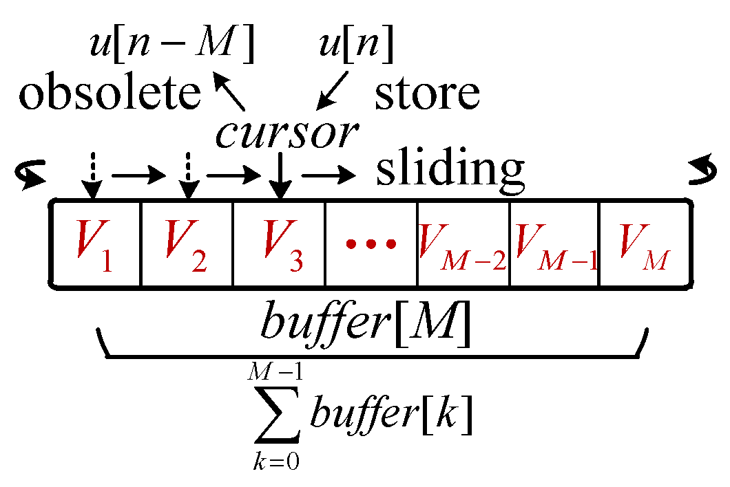
In the practical experiment and application, the moving average filter is implemented in the controller as illustrated in
Figure 11. A memory array
buffer[
M] of length M is allocated in the heap, and a pointer cursor tracks the oldest data
u[
n−
M].
The sum ∑buffer[k] is updated incrementally: the oldest value is replaced by the latest input u[n], and cursor is advanced to the next element. When cursor reaches the end of the array, it wraps around to form a circular buffer. The filter output is then given by ∑buffer[k]/M. During the first 200 points, the average gradually converges as the window fills. Afterward, each update requires only one addition and one subtraction, significantly improving computational efficiency compared with summing all 200 points at each step.
The frequency response of the moving average filter is given by
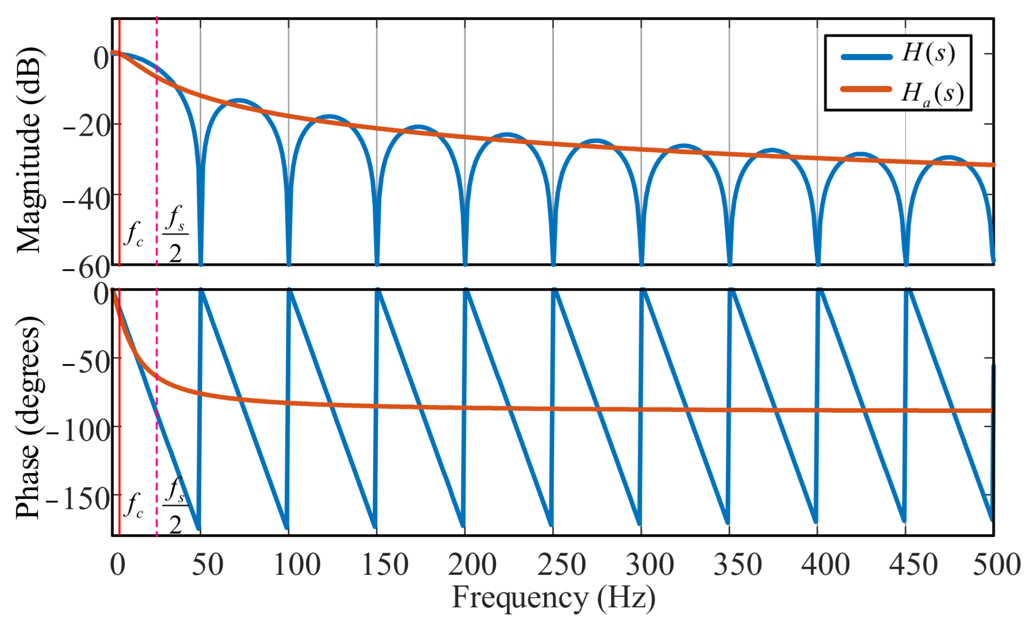
As shown in
Figure 12 the Bode plot, zeros appear successively at 50 Hz and its harmonics. Therefore, the moving average filter provides complete attenuation at 50 Hz and its integer multiples.
In this paper, the controller design was carried out using the root locus method. However, since the frequency response of the moving average filter corresponds to a Dirichlet kernel, directly applying the root locus analysis to the
z-domain transfer function in (14) is intractable. To address this problem, the moving average filter is approximated in the low-frequency range of the Nyquist frequency as a first-order inertia transfer. Specifically, yielding the following approximation:
In the low-frequency range, this first-order inertia approximation can effectively emulate the dynamic characteristics of the moving average filter as in
Figure 12. Therefore, in both the experimental and simulation stages of designing phase-level capacitor voltages controller
Dp(
z) and arm-level capacitor voltage controller
Da(
z), the approximate inertia element
Ha(
s) was employed in place of the moving average filter for controller parameter design.
3.3.2. Phase-Level Capacitor Voltages Control
According to the small-signal equivalent circuit of the common-mode voltage in
Figure 8, a differential relationship exists between the applied common-mode voltage
and the resulting common-mode current
as
Which can be expressed by the transfer function
Applying a zero-order-hold (ZOH) discretization to (19) with sampling period
Ts = 0.02 s yields the following
z-domain discrete transfer function:
Since the discrete sampling period coincides with the fundamental-frequency period, and the output of the controlled plant remains constant within each ZOH interval, the control input in (20) can be regarded as its DC component , while the output can similarly be considered as its DC component .
Furthermore, the sum of the modulation voltages of the upper and lower arms in the same phase equals
Udc. The product of the DC component of the common-mode current
and the sum of the upper- and lower-arm output voltages
Udc corresponds to the phase-regulating power
, which is used to charge the capacitors across the entire phase.
Additionally, a small-signal transfer function can be derived for the phase capacitor charging process in (20).
By applying ZOH discretization to (20) with a sampling period of
Ts = 0.02 s, the discrete transfer function from the modulation voltage
to the total capacitor voltage
of the upper and lower arms is established, as illustrated in
Figure 13.
In
Figure 13, the discretized transfer functions are denoted as
and
, respectively.
As illustrated in
Figure 14, a discrete controller,
Dp(
z), and a moving average filter,
H(
z), are introduced to implement closed-loop control of the plant.
The discrete controller Dp(z) is implemented as a PI controller and discretized using the Tustin method. Through Dp(z), the system can maintain the DC component of the common-mode current, thereby regulating the average capacitor voltage of the phase. Combined with the moving average filter H(z), the controller extracts the DC component of the arm capacitor power and provides feedback for closed-loop regulation, ensuring that the upper- and lower-arm capacitor voltages under varying operating conditions.
The PI controller in the discrete domain is designed using the Tustin transformation, as expressed
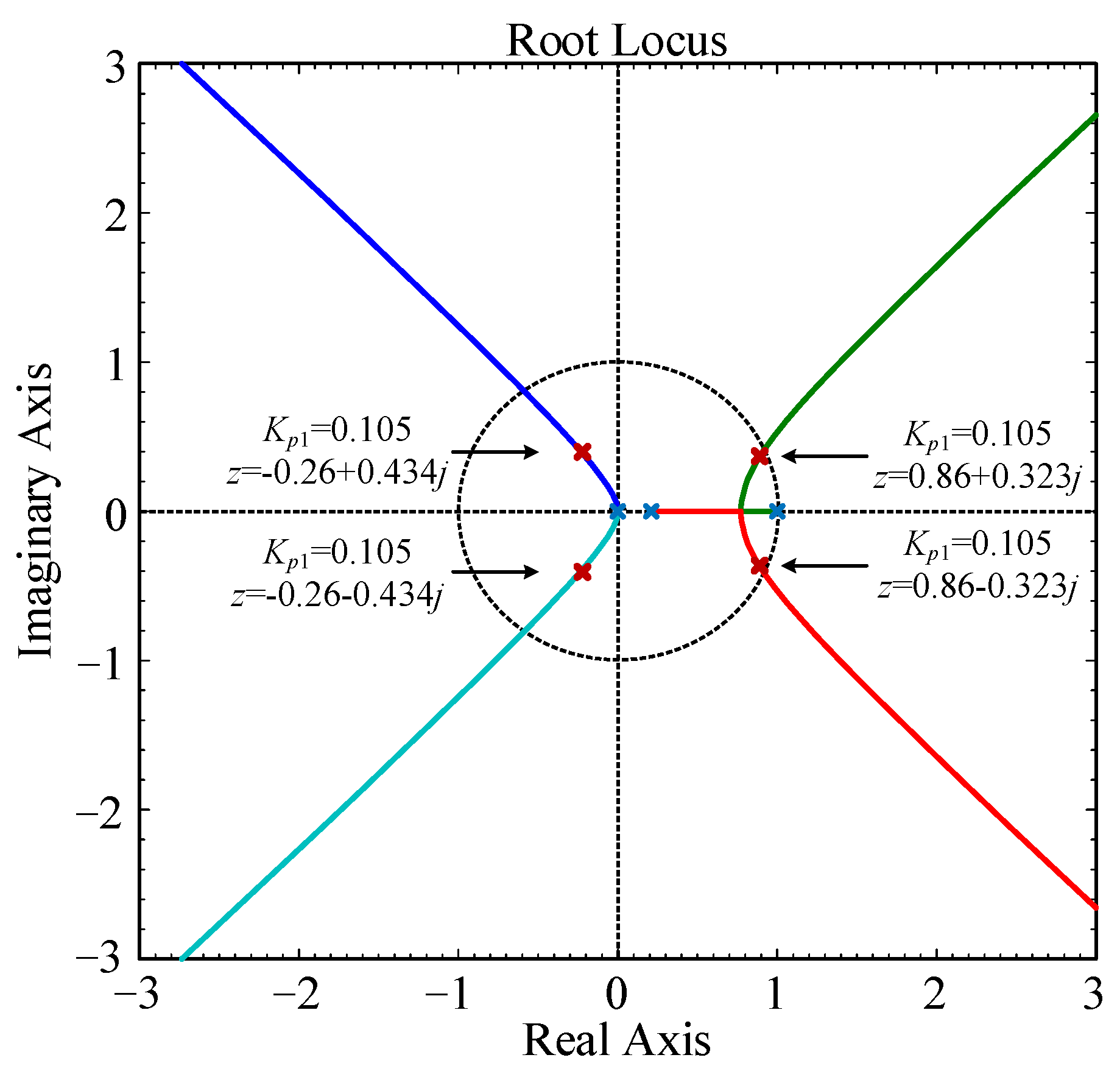
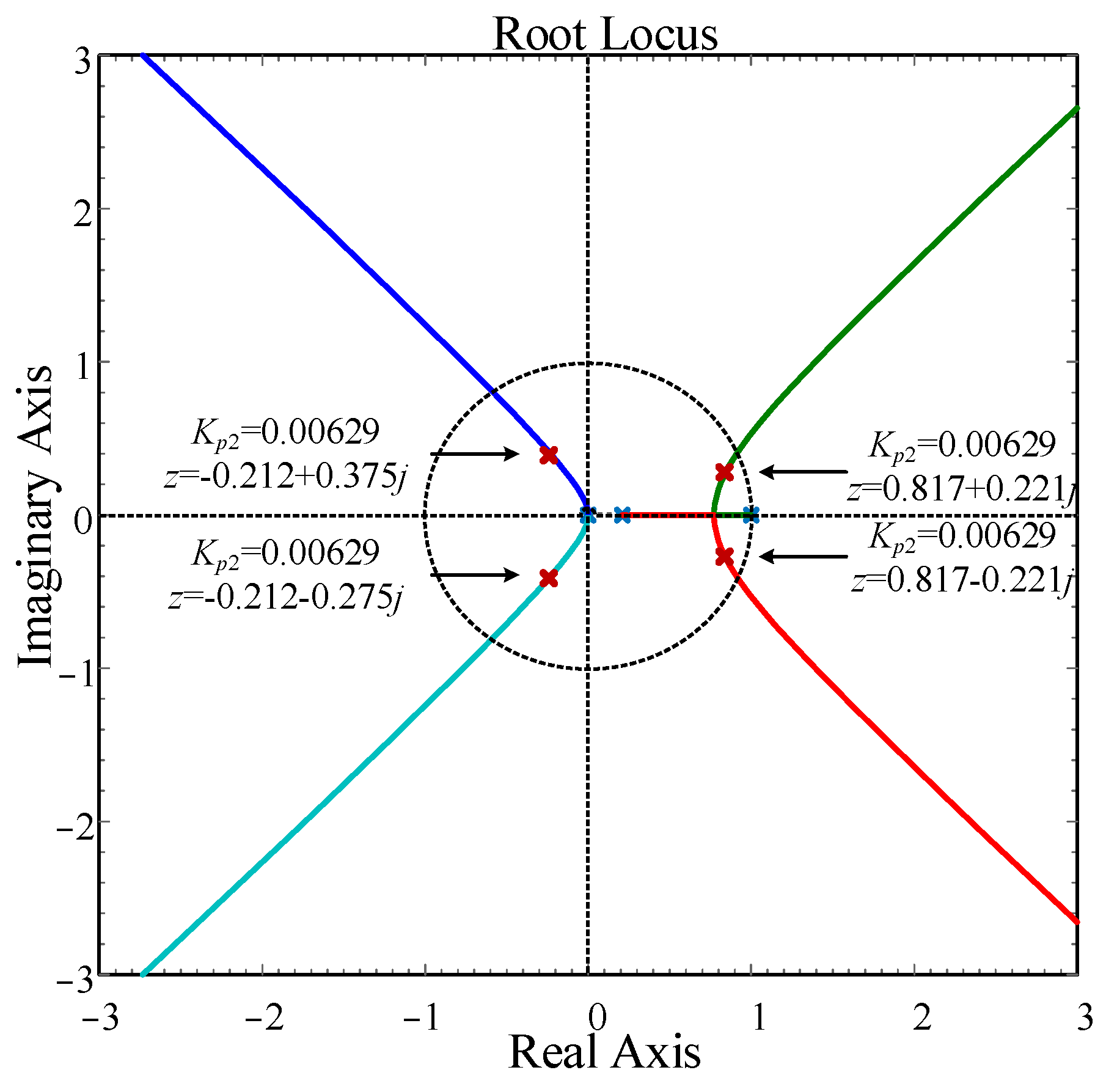
Taking the simulation parameters as an example, by substituting them into the model, the root locus under the discrete control period of
Ts = 0.02 s is obtained
Figure 15. It shows the root locus of the
Dp(
z) controller as the proportional gain kp1 varies from 0 to ∞. The discrete system is stable when the poles remain inside the unit circle.
3.3.3. Arm-Level Capacitor Voltage Control
The core of the upper- and lower-arm capacitor voltage balancing control lies in regulating the phase shift angle
(
t) of the fundamental common-mode voltage
(
t) with respect to the differential voltage
(
t). This adjustment enables the synchronization angle
(
t) of the fundamental common-mode current
(
t) to be controlled. The small-signal equations of the common-mode voltage and current are expressed in (19).
Evidently, the differential equation from
to
involves nonlinear trigonometric terms, which cannot be linearized by separating the steady-state operating point.
Considering that, under steady-state conditions in
Figure 8,
=
, the process from the voltage phase-shift angle to the current synchronization angle is simplified as an inductive inertia element with a static gain of unity, as expressed in (20).
Furthermore, the term can be simplified at the steady-state operating point in (25).
Applying the ZOH discretization to (20) and (24) with a sampling period of
Ts = 0.02 s, the discrete transfer function from the small-signal phase-shifting angle
to the voltage difference
between the upper and lower arms is obtained, as shown in
Figure 16.
The discrete transfer functions in the z-domain are denoted as and .
Figure 17 illustrates the block diagram of the closed-loop control scheme for balancing the capacitor voltages between the upper and lower arms.
Da(
z) is the PI controller for capacitor voltage balance between arms. The control objective is to suppress voltage imbalance
by regulating the phase angle
(
t) of the fundamental common-mode voltage
(
t) with respect to the differential voltage
(
t). Through this mechanism, the synchronization angle of the common-mode current
(
t) is adjusted, thereby achieving an effective redistribution of power between the arms and maintaining capacitor voltage balance.
Similarly, for the upper and lower arm voltage balancing control, the discrete controller is designed using a PI structure with Tustin transformation, as expressed
By substituting the simulation parameters, the root locus under a discrete control period of
Ts = 0.02 s is obtained in
Figure 18.
Figure 18 shows the root locus of the
Da(
z) controller as the proportional gain
kp2 varies from 0 to ∞. The discrete system is stable when the poles remain inside the unit circle.
4. Simulation Verification
To verify the effectiveness of the proposed capacitor voltage balancing control method based on self-synchronized common-mode current, detailed simulations were conducted using the software platform.
The simulation model is established based on a 10 kV distribution network. Each arm consists of four high-voltage MMC submodules rated at 4.5 kV, with a submodule capacitance of 2000 μF. The CPS-PWM modulation strategy is applied to each submodule. The DC bus voltage is set to 18 kV. The arm inductance
La is designed to be 10 mH with an equivalent resistance
Ra of 4 Ω. The detailed simulation parameters are summarized in
Table 1.
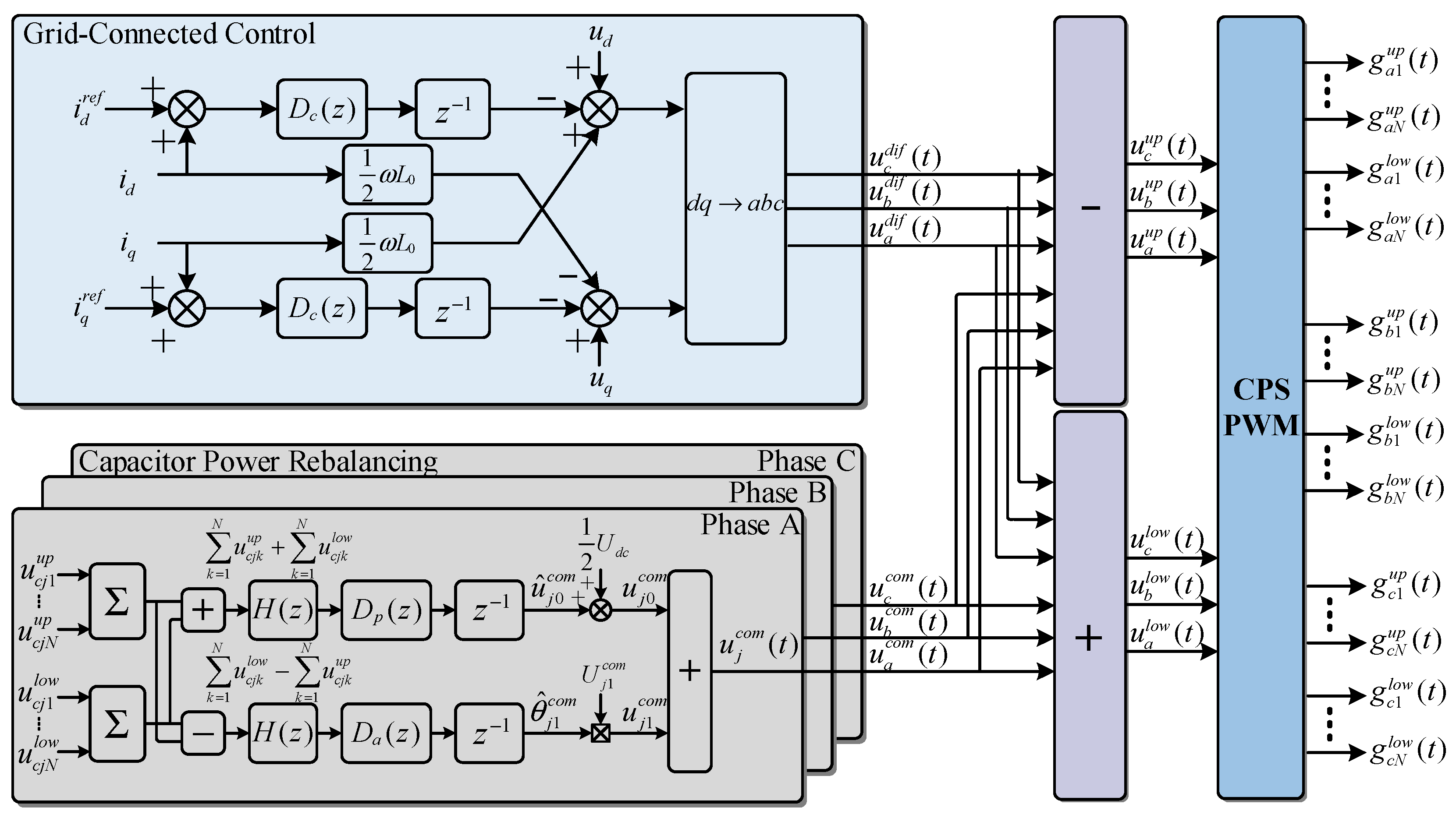
Figure 19 shows the control system structure. The instantaneous reactive power control is adopted on the AC side, with the d-axis current reference set to 30 A and the q-axis current reference set to 0 A. The capacitor power rebalancing control is implemented on a per-phase basis, where the sum and difference in the upper and lower arm capacitor voltages are regulated to generate the common-mode modulation voltage
(
t). This voltage is then superimposed with
(
t) and modulated using CPS-PWM, producing the phase-shifted switching signals for each submodule. The control parameters in
Figure 19 are listed in
Table 2.
The simulation results are presented in
Figure 20,
Figure 21,
Figure 22,
Figure 23,
Figure 24 and
Figure 25. These figures illustrate the performance of the proposed control scheme in terms of grid-connected operation, capacitor voltage balancing, common-mode current synchronization, and dynamic response under different operating conditions.
Figure 20 illustrates the grid-side current waveforms of the ES-MMC in the three-phase stationary
abc reference frame. Since the instantaneous reactive power control method is adopted with the d-axis current reference set to 30 A, the amplitude of the grid current is regulated to 30 A and remains in phase with the corresponding grid voltage.
Figure 20a shows the long-term steady-state current waveform, where the grid current is stably maintained.
Figure 20b presents the locally magnified waveform, confirming the sinusoidal characteristics of the CPS-PWM 10 kHz.
Figure 20c illustrates the closed-loop control result of the d-axis current, which accurately tracks the 30 A reference.
Figure 20d shows the closed-loop result of the q-axis current, which is effectively regulated to 0 A, demonstrating successful decoupled active and reactive current control.
Figure 21 shows the capacitor voltage waveforms of Phase A, where each upper and lower arm consists of eight submodule capacitors.
Figure 21a illustrates the entire simulation process, which is divided into four stages (I–IV). In Stage I, the system operates in grid-connected mode, and the capacitor balancing control is not activated,
(
t) = 0,
= 0. In Stage II,
is set to 50 V, which introduces a corresponding common-mode circulating current component in the arms. As a result, the capacitor voltages exhibit larger fluctuations, as shown in
Figure 21b.
In Stage III, an unbalanced power injection of 4.5 kW = 4.5 kV × 1 A is applied to the second submodule of the upper arm. Since the capacitor voltages within the same arm are regulated by the proportional control method proposed in [
9], the voltages stabilize at levels proportional to the deviation in average power. Consequently, the second submodule voltage stabilizes around 4700 V due to its higher output power, while the other capacitor voltages in the upper arm are lower than the average voltage of the lower arm.
In Stage IV, when the injected power from the energy storage side is removed, the power balance among all submodules is restored, and the capacitor voltages of both upper and lower arms immediately recover to a balanced state.
Figure 22 shows the average voltage control of the upper and lower arms, which corresponds to the regulation of the DC component
(
t) of the common-mode voltage.
Figure 22a illustrates the moving-averaged capacitor voltages of the upper and lower arms. In Stages I and II, without closed-loop control, the arm capacitor voltages slightly deviate from the rated value of 18 kV. In Stage III, after the common-mode voltage controller is activated, the average voltages of both arms are effectively compensated and stabilized at 18 kV.
Figure 22b compares the moving-averaged capacitor voltage with the raw waveform. Due to the influence of the differential-mode current and common-mode current on the AC side, the raw capacitor voltage exhibits significant fluctuations. By applying a moving average filter with a sampling period of
Ts = 0.02 s, the pulsating components are effectively suppressed, thereby avoiding adverse effects on the control performance.
Figure 23 illustrates the differential capacitor voltages between the upper and lower arms, which reflect the relative voltage deviation within each phase.
Figure 23a shows the moving-averaged differential voltages over the simulation period. In Stages II, without closed-loop compensation but, the differential voltages exhibit noticeable deviations from zero, indicating voltage imbalance between the upper and lower arms. When the common-mode voltage controller is activated in Stage III, the differential voltages are effectively suppressed and converge close to zero, demonstrating successful balancing of the arm capacitor voltages.
Figure 23b compares the moving-averaged differential voltages with the raw differential waveforms. The raw signals contain fluctuations induced by the AC-side differential-mode and common-mode currents. By applying a moving average filter with a sampling period of
Ts = 0.02 s, the pulsating components are smoothed, which avoids interference with the voltage balancing control.
Figure 24 illustrates the variation in the synchronization angle between the common-mode current
(
t) and the differential voltage
(
t) of phase
a.
Figure 24a presents the steady-state time-domain waveform. At steady state, the capacitor voltages of the upper and lower arms are balanced, resulting in no active power exchange between the arms. According to (13) and
Figure 10, synchronization angle
equals 0.5π.
Figure 24b shows the variation in the synchronization angle over different simulation stages. In Stage I, since
= 0, the common-mode current
(
t) = 0, and the synchronization angle exhibits random fluctuations with no practical significance. In Stage II, with
= 50 V, the synchronization angle stabilizes near the steady-state point of 0.5π. In Stage III, to compensate for the unbalanced power output between the upper and lower arms, the synchronization angle
deviates from the steady-state point. In Stage IV, after the external energy injection from all submodules is balanced, the synchronization angle returns close to the steady-state value.
The behaviors in
Figure 22 and
Figure 23 are mutually coupled. Through the closed-loop distribution of common-mode and differential-mode power, the control strategy compensates for the unbalanced power output of the submodule energy storage units, ensuring stable capacitor voltage regulation.
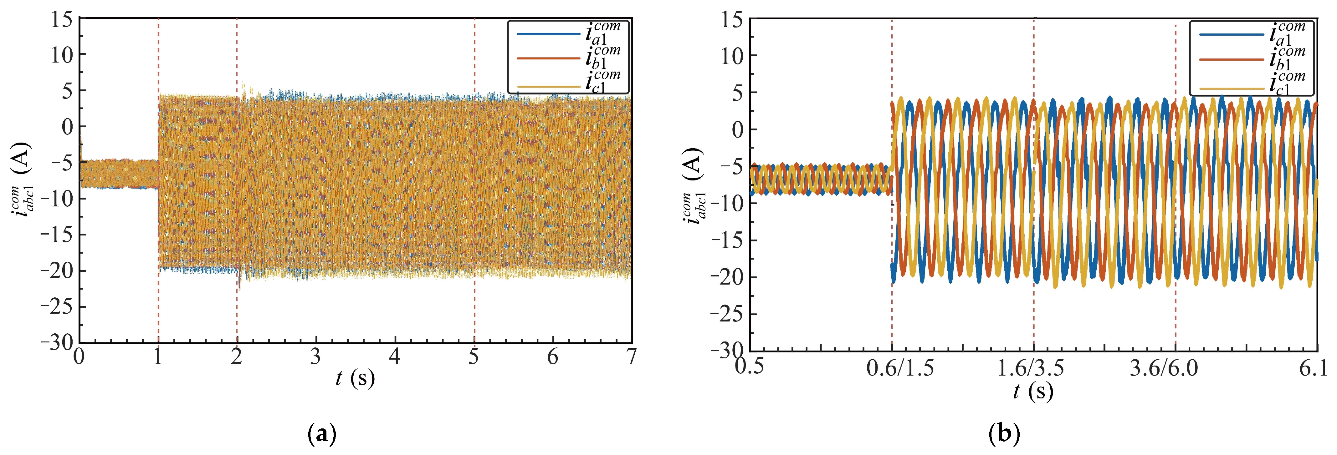
Figure 25 shows the fundamental-frequency common-mode currents
,
, and
in the three-phase system.
Figure 25a presents the time-domain waveforms over the entire simulation. In Stage I, the fundamental common-mode currents are primarily caused by fluctuations in the submodule capacitor voltages. From Stages II to IV, after superimposing the common-mode voltage
= 50 V, the fundamental common-mode currents reach an amplitude of approximately 22 A.
Figure 25b shows a locally magnified view of the waveforms, highlighting the dynamics of the common-mode currents in each stage.
These results demonstrate that the proposed common-mode voltage injection effectively generates controllable fundamental-frequency common-mode currents, which play a key role in compensating power imbalances among the arms in the same phase and maintaining capacitor voltage equilibrium.
Under rated operating conditions, the capacitor voltages of the upper and lower arms remain well balanced, demonstrating that the proposed self-synchronized common-mode current control strategy maintains steady-state performance. When unbalanced power conditions are introduced among the energy storage units, transient voltage deviations occur. However, the proposed method rapidly regulates the capacitor voltages, effectively restoring balance and ensuring system stability. These results confirm the robustness and effectiveness of the control approach under both nominal and disturbed operating scenarios.
5. Experimental Validation
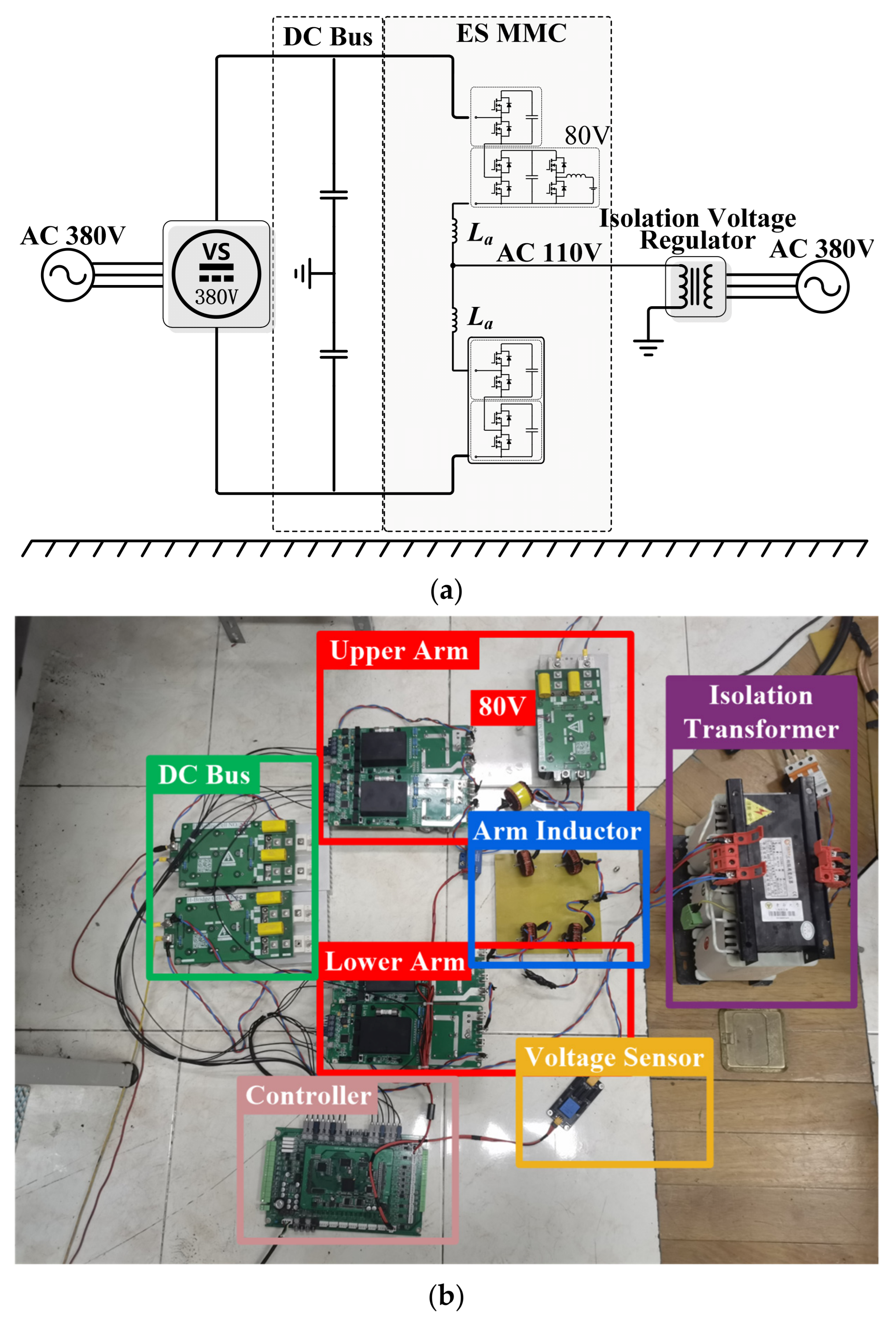
To further verify the effectiveness of the proposed self-synchronized common-mode current control strategy for achieving power balancing in both upper and lower arms, a single-phase ES-MMC experimental prototype was developed. The prototype is implemented using SiC MOSFET H-bridge submodules.
An experimental platform for a single-phase ES-MMC prototype was developed, as illustrated in
Figure 26. The prototype consists of four H-bridge submodules, each implemented with SiC MOSFETs, and is equipped with a 1000 µF dc-link capacitor. It is connected to distributed low-voltage storage units through bidirectional DC/DC interfaces. The system is rated at a DC bus voltage of 400 V, with an AC-side rated voltage of 110 V and an output current of 0 A. Thus, the AC-side differential voltage
is in phase with the grid voltage. Each arm is equipped with a 4 mH inductor
La and a series resistance
Ra of approximately 0.5 Ω to suppress circulating current. Circuit parameters are listed in
Table 3.
The control system is implemented on a digital signal processor (DSP, TMS320F28335), where the voltage and current signals are measured by Hall-effect sensors and fed into the DSP via isolated signal conditioning circuits. CPS-PWM is employed, with phase-shifted carriers generated and distributed by the DSP. This setup enables comprehensive experimental verification of the proposed self-synchronized common-mode current control strategy under various operating conditions.
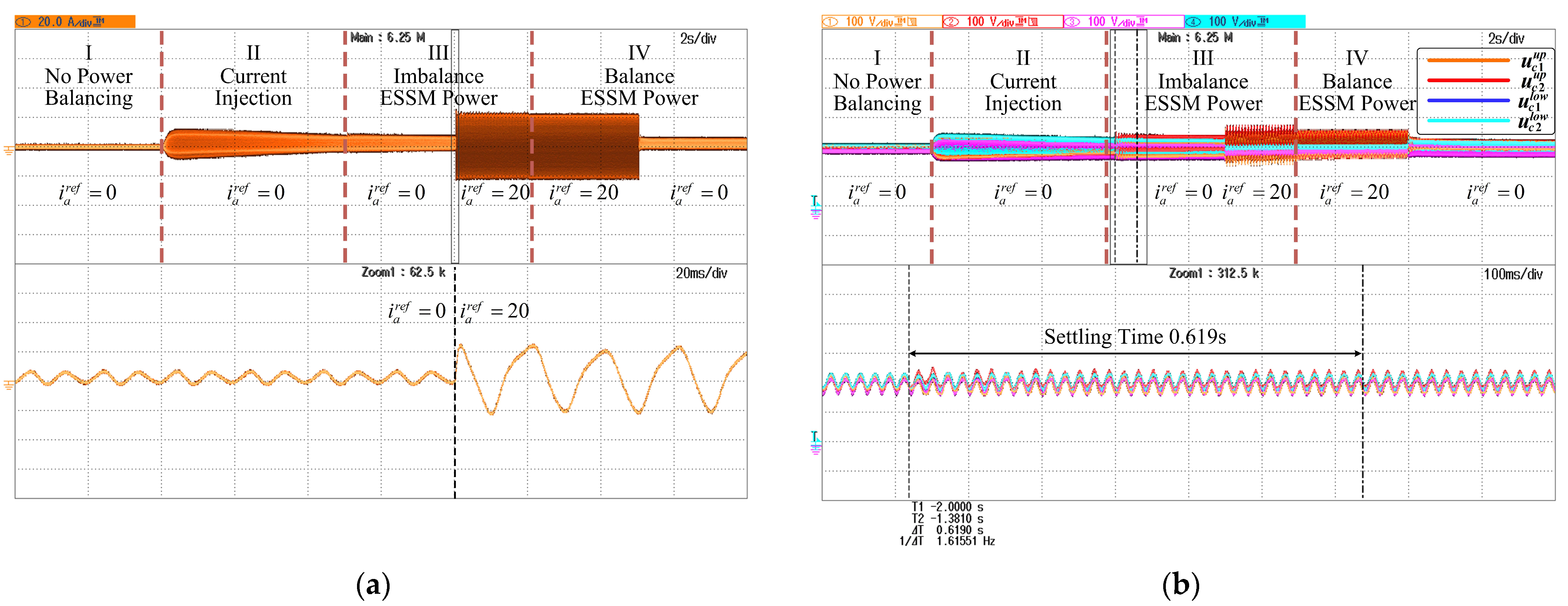
Figure 27a shows the ac-side current
ia(
t), which is set to 0 A. In this condition, no current flows through the arm inductors, and the voltages across the inductors are equal. Consequently, the differential modulation voltage of the upper and lower arms,
(
t), is identical to the grid voltage
ua(
t). Therefore, the grid voltage
ua(
t) can be directly measured instead of
(
t). This substitution is necessary because the differential modulation voltage is essentially a control signal that cannot be directly measured, whereas
(
t) serves as the reference for the synchronization angle, which is indispensable for the study.
Figure 27b illustrates the waveforms of four submodule capacitor voltages, namely
,
,
, and
. In Stage I, without capacitor voltage balancing control, the capacitor voltages remain stable. In Stage II, when the common-mode current is injected, the fluctuations in capacitor voltage increase. In Stage III, an additional power of 200 W (200 V × 1 A) is injected into the second submodule of the upper arm through the buck–boost converter, leading to a higher average voltage of
compared with the others. The settling time after introducing power imbalances is about 0.619 s. The AC grid current increases from 0 to 20 A. In Stage IV, after the additional power injection is removed, the capacitor voltages of both arms recover to balance, as the grid current amplitude decreases from 20 A to 0.
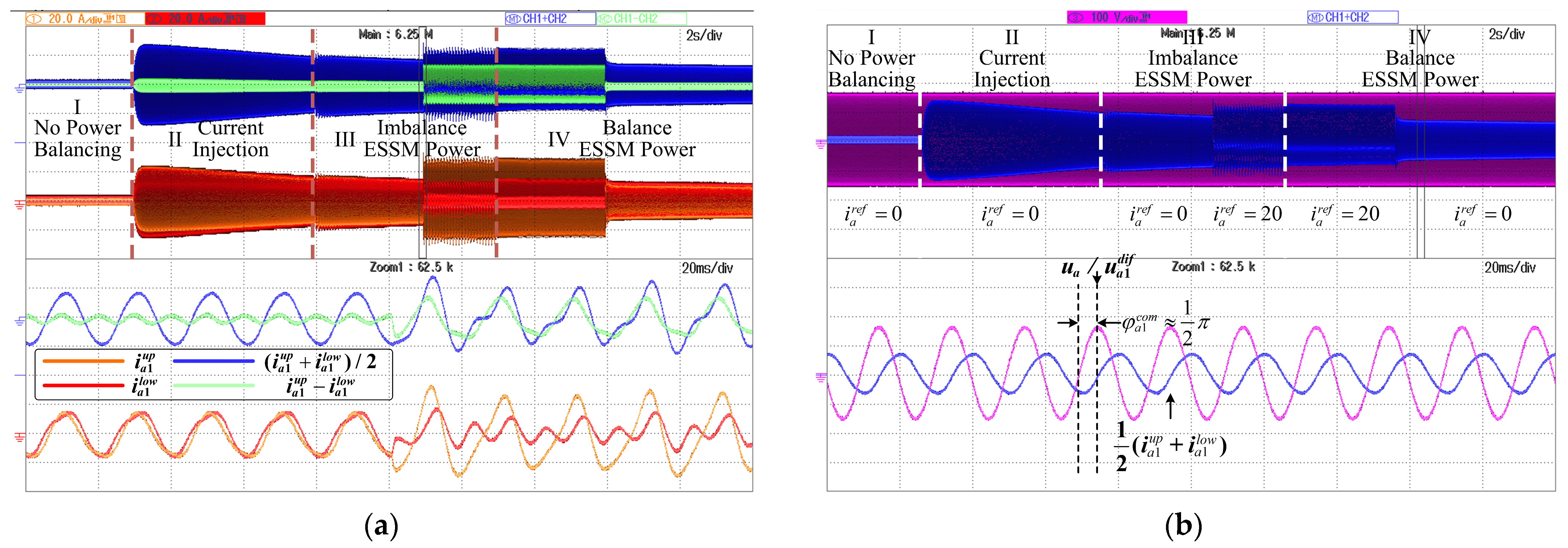
Figure 28 presents the common-mode current. Since the oscilloscope cannot directly calculate the average value, the sum of the upper- and lower-arm currents, (
+
)/2 =
, is adopted as a substitute, which corresponds to twice the actual amplitude of the common-mode current. In
Figure 28a, the common-mode current remains relatively small in Stage I. The common-mode voltage is injected in Stage II, and its amplitude increases. In Stage III, when additional power is injected into
, the phase of
shifts accordingly. In Stage IV, as power balance is reestablished, the system reaches steady-state operation.
Figure 28b depicts the steady-state common-mode current and the grid voltage
ua in Stage IV. Since the AC side current is set to 0 A, it can be approximated that
≈
ua. Under this condition, the synchronization angle in the steady state is 0.5π.
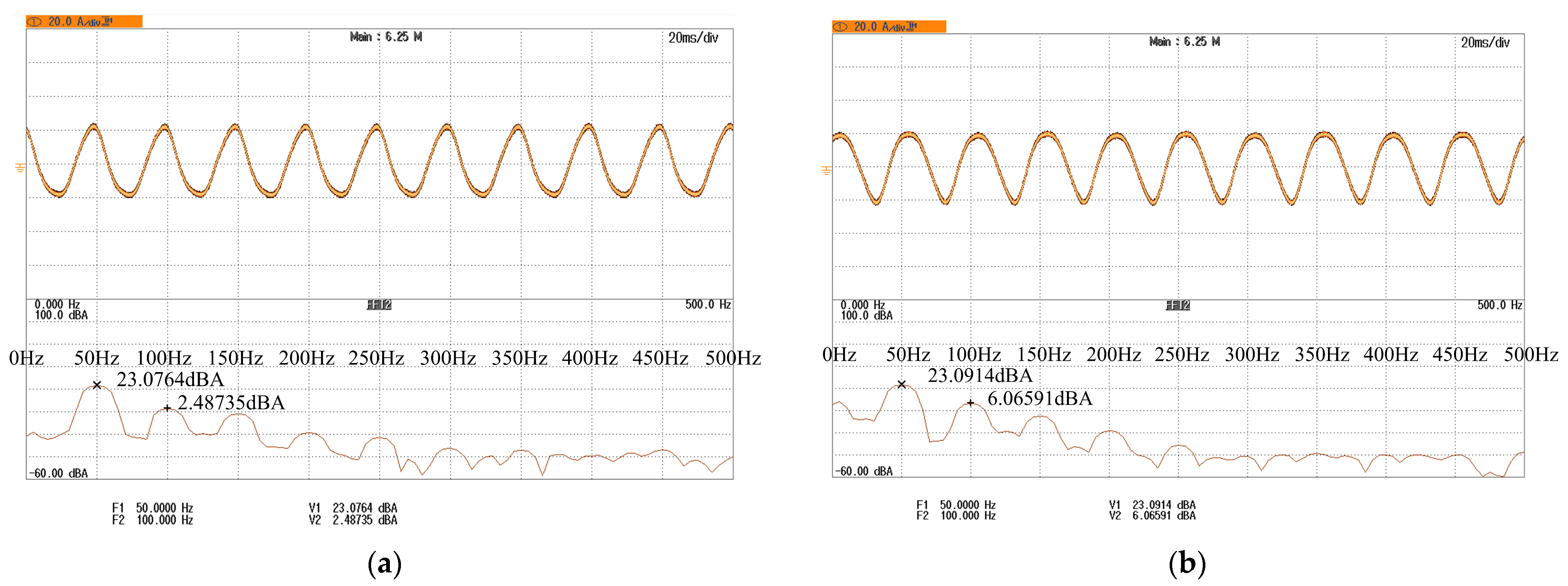
Figure 29 presents the FFT-based THD analysis of the grid current
ia = 20 A, measured by an oscilloscope. The FFT is performed with respect to the 50 Hz and its harmonics. The dominant component of the grid current is the 50 Hz, which remains nearly unchanged before and after applying the proposed capacitor voltage balancing algorithm (23.0764 dBA vs. 23.0914 dBA). In contrast, the second-order harmonic increases from 2.48735 dBA to 6.06591 dBA when the control algorithm is enabled.
This increase is likely attributed to the introduced common-mode current, which induces a fundamental-frequency voltage fluctuation on the submodule capacitors. Through modulation, this fluctuation is coupled into the grid current ia, leading to a slight rise in the second-order harmonic. Overall, the proposed capacitor voltage balancing algorithm has a negligible impact on the grid current THD.
To verify the accuracy of the experimental results, simulations were conducted based on the circuit parameters listed in
Table 3. The simulated waveforms in
Figure 30a–f correspond to the experimental results in
Figure 27 and
Figure 28.
Overall, the simulation results are consistent with the experimental results I–IV. However, due to practical environmental factors and differences in controller implementation, slight discrepancies exist between the experimental and theoretical waveforms. In the experiments, the circulating current is lower than the theoretical value and is significantly affected by the grid-side AC current, resulting in waveform distortion, whereas the simulations exhibit more ideal behaviors.
