Abstract
Among other uses, DC-DC converters are employed in the auxiliary power modules (APMs) of electric vehicles (EVs), connecting the high-voltage traction battery to the low-voltage auxiliary system (AS). Traditionally, the APM is an isolated two-port, two-level (2L) DC-DC converter, and the auxiliary loads are fed at a fixed voltage level, e.g., 12 V in passenger cars. Dual-active-bridge (DAB) converters are commonly used for this application, as they provide galvanic isolation, high power density and efficiency, and bidirectional power flow capability. However, the auxiliary loads do not present a uniform optimum supply voltage, hindering overall efficiency. Thus, a more flexible approach, providing multiple supply voltages, would be more suitable for this application. Multiport DC-DC converters capable of feeding auxiliary loads at different voltage levels are a promising alternative. Multilevel neutral-point-clamped (NPC) DAB converters offer several advantages compared to conventional two-level (2L) ones, such as greater efficiency, reduced voltage stress, and enhanced scalability. The series connection of the NPC DC-link capacitors enables a multiport configuration without additional conversion stages. Moreover, the modular nature of the ML NPC DAB converter enables scalability while using semiconductors with the same voltage rating and without requiring additional passive components, thereby enhancing the converter’s power density and efficiency. This paper proposes a modulation strategy and decoupled closed-loop control strategy for the generalized multiport 2L-NL NPC DAB converter interfacing the EV traction battery with the AS, and its performance is validated through hardware-in-the-loop testing and simulations. The proposed modulation strategy minimizes conduction losses in the converter, and the control strategy effectively regulates the LV battery modules’ states of charge (SoC) by varying the required SoC and the power sunk by the LV loads, with the system stabilizing in less than 0.5 s in both scenarios.
1. Introduction
One of the major challenges of the climate emergency is the electrification of mobility systems on a global scale. The transport sector is responsible for one-fifth of carbon emissions worldwide [1], with road transport representing over 70% of the sector’s total emissions [2]. In response, global organizations are promoting the use of electric vehicles (EVs) in order to meet the growth in road transport demand while reducing their environmental impact. Notably, as a result of the measures included in the European Green Deal [3], EVs are projected to account for 80% of the total vehicles in use in Europe by 2050.
Figure 1 illustrates the typical electrical scheme of an EV. The on-board charger connects the AC charging port to the EV’s traction battery through its common high-voltage (HV) DC bus. The EV’s electric motor is then connected to the HV traction battery modules through a DC-AC converter. The EV auxiliary system (AS), comprising the low-voltage (LV) auxiliary battery and loads, is powered by the traction battery through the auxiliary power module (APM), interfacing the LV and HV DC buses.
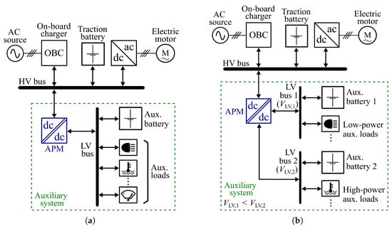
Figure 1.
Electrical scheme of an EV. (a) Using a single-voltage AS architecture. (b) Using a dual-voltage AS architecture.
Traditionally, the APM is a two-port DC-DC converter, and the auxiliary battery and loads are connected to its LV side, operating at a single voltage value, typically 12 V for passenger cars [4], as depicted in Figure 1a. The use of a bidirectional dual-active-bridge (DAB) DC-DC converter for this application is common, as it provides galvanic isolation, high power density, high efficiency, and the ability to transfer power in both directions [5,6,7,8,9].
However, the EV auxiliary loads do not present homogeneous power consumption. Loads such as electronic control units and infotainment systems are classified as low-power loads, whereas the powertrain cooling system, lighting, hydraulic brake system, windshield and window motors, and autonomous driving systems are considered high-power loads. By feeding high-power loads at a higher voltage than low-power loads, the current consumption and the required cabling cross-section are reduced, resulting in lower losses, cost, and weight. On the other hand, some low-power loads are supplied through a secondary converter, stepping down the voltage from 12 V to 5 V or 3.3 V. Then, feeding the low-power loads from lower-voltage DC ports allows reducing the voltage reduction factor of the secondary converter, which improves efficiency and power density. Furthermore, the increasing demand for vehicle amenities drives manufacturers to incorporate more features to enhance the EV’s appeal to the public, which translates into more LV loads in the AS with an increasing variety of optimum operating voltages.
In this context, a multiple-voltage architecture is an effective solution for the AS. Figure 1b depicts the electrical scheme of an EV using a dual-voltage architecture. In this configuration, the low-power auxiliary loads are connected to the lower-voltage LV bus 1, operating at , whereas the high-power auxiliary loads are connected to the higher-voltage LV bus 2, operating at , with . This multiple-voltage structure uses two auxiliary batteries operating at different voltage levels and requires the integration of multiple DC ports rated at different voltages within the APM.
Multiport DC-DC converters (MPCs) are a suitable option for the APM in EVs with a multiple-voltage architecture in their AS [10]. Several MPC topologies have been proposed in the literature for this purpose [11,12,13,14,15,16,17,18,19,20,21,22]. These topologies are different variations of two-port, two-level (2L) isolated DC-DC converters that form MPCs. Some proposed topologies, such as the triple active bridge (TAB) proposed in [11], the resonant three-port converters presented in [12,13], the cascaded DC-DC converter proposed in [14], or the interleaved dual floating current-fed DAB converter presented in [15], add an additional full-bridge cell to obtain a three-port connection. Alternatively, new three-port and four-port isolated DC-DC topologies can be obtained by integrating additional passive components into the two-port 2L DAB converter [16,19,20,22], by modifying the configuration of the converter’s active switches and diodes [17,18], or by combining multiple 2L DC-DC converter topologies [21]. These topologies enable the use of multiple LV batteries in the AS operating at different voltage levels and present different trade-offs among reduced overall losses, power density, and the control of power flow between the different ports.
The use of multilevel (ML) DAB converters is an alternative approach for the design of a multiport APM. The most studied topology for multilevel (ML) DAB converters is the neutral-point-clamped (NPC) [23], mainly due to its great compactness, power density, and efficiency, which are highly beneficial features in EVs. Furthermore, the series connection of the DC-link capacitors in an NPC DAB converter can be employed to obtain multiple DC ports with different voltage levels, resulting in a multiport DC-DC single-stage converter, i.e., without requiring additional conversion stages to obtain multiple DC ports. The 3L NPC DAB converter has been studied in recent years for multiport applications. For instance, the use of a multiport 2L-3L NPC DAB converter was proposed in [24,25,26] for controlling the voltage balance in bipolar LV and MV DC distribution systems. However, no studies have investigated 4L or higher-level NPC DAB converters in single-stage multiport configurations.
Figure 2a illustrates the proposed connection of the EV AS to the traction battery () using a multiport 2L-3L NPC DAB converter, with the converter legs depicted as single-pole double-throw (SP-2T) and single-pole triple-throw (SP-3T) switches at the HV and LV sides, respectively. At the LV side, the connection uses the two DC ports to supply two 12-V battery modules ( and ) and the LV loads. The battery modules are connected between consecutive nodes of the 3L DC link. The auxiliary loads are divided into two main groups: low-power loads, connected to the 12-V rail of the LV DC link (between nodes and ), and high-power loads, connected to the 24-V rail (between nodes and ).
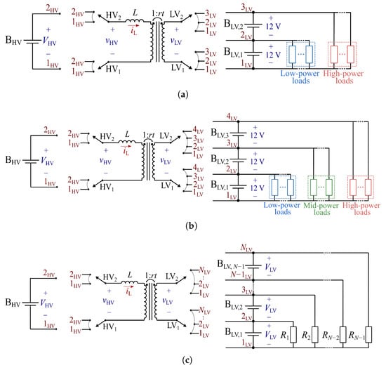
Figure 2.
Connection of the traction battery and the AS to the APM. (a) Using a multiport 2L-3L NPC DAB converter. (b) Using a multiport 2L-4L NPC DAB converter. (c) Using a multiport 2L-NL NPC DAB converter.
Expanding on this concept, Figure 2b illustrates the proposed connection using a multiport 2L-4L NPC DAB converter. The converter uses three DC ports to supply three 12-V battery modules, each connected between consecutive nodes of the converter’s 4L DC link. Then, auxiliary loads are connected either to the 36-V rail (between nodes and ), the 24-V rail (between nodes and ), or the 12-V rail (between nodes and ), depending on their optimal voltage supply values.
Thus, by increasing the number of levels of the multiport NPC DAB converter, a higher number of 12-V battery modules can be connected between the nodes of the ML DC link. This results in a higher voltage across the end terminals of the DC link and provides more DC ports with partial voltage levels. The modular nature of the proposed connection then enables scalability while using the same voltage-rated semiconductors across all configurations. Furthermore, multiple voltage levels are achieved by stacking the battery modules of the same operating voltage in series, avoiding the need for different battery models and thus further simplifying the system design.
Following this approach, this paper proposes a novel generalized connection of LV battery modules and auxiliary loads to a multiport 2L-NL NPC DAB converter. This configuration is illustrated in Figure 2c and can be implemented using different topologies of NPC legs, such as the diode-clamped NPC, the active NPC (ANPC), or the T-type NPC, as presented in [27] and depicted in Figure 3.
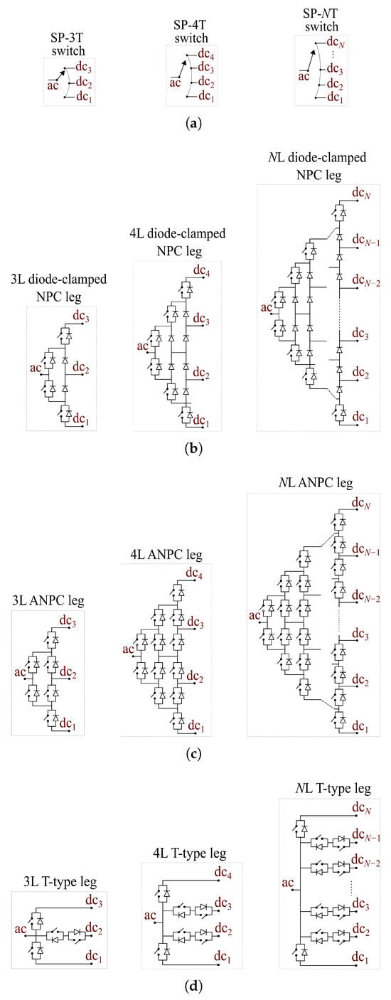
Figure 3.
Topologies of NPC legs. (a) SP-4T, SP-4T, and SP-NT switch representations of NPC legs. (b) 3L, 4L, and NL diode-clamped NPCs. (c) 3L, 4L, and NL ANPCs. (d) 3L, 4L, and NL T-type legs.
In the proposed connection, the power sunk by the loads connected to the partial-voltage DC ports imposes an unbalanced power sourcing from the LV battery modules, which must be compensated through appropriate converter operation. To overcome this challenge, the electric currents in the NL-side DC link are analyzed, and a generalized modulation strategy and a closed-loop control strategy are proposed, effectively regulating the state of charge (SoC) of the LV battery modules while ensuring a wide range of power-supply distribution to the loads.
The rest of this paper is organized as follows. Section 2 introduces the generalized modulation strategy for the multiport 2L-NL NPC DAB converter. Section 3 presents the proposed strategy for controlling the SoC of the auxiliary battery modules. Section 4 introduces a decoupling approach for the control. Section 5 details the results obtained through hardware-in-the-loop (HIL) tests and MATLAB/Simulink simulations. Finally, Section 6 discusses the relevance of the proposed connection and control strategy and outlines future research work.
2. Generalized Modulation Strategy for the Multiport 2L-NL NPC DAB Converter
2.1. Analysis of NL-Side DC Link Currents
To define an effective modulation strategy for the multiport 2L-NL NPC DAB converter, an analysis of the electrical currents in the NL-side DC link must be performed.
Figure 4a presents the connection of the loads and to the nodes and of the LV-side DC link of the 2L-3L NPC DAB converter. Currents and are injected by the converter into nodes and , respectively, while and are sunk by loads and , respectively. The expressions for the average currents over a switching period in the battery modules, and , can be obtained by applying the Kirchhoff current law (KCL) to nodes and , and are
where and are the average values over a switching cycle of and , respectively.
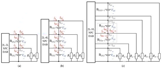
Figure 4.
Connection of the auxiliary loads to the NPC DC link. (a) Using a 2L-3L NPC DAB converter. (b) Using a 2L-4L NPC DAB converter. (c) Using a 2L-NL NPC DAB converter.
Expanding this concept to the 2L-4L NPC DAB converter (Figure 4b), the expressions for the battery average currents are
From Equations (1) and (2), the generalized expression for the average current in the nth LV battery module of an NL DC link is obtained following an inductive process and is
To guarantee the power supply to the loads, it is necessary to ensure that the batteries’ SoC variation is minimum or even zero, i.e., the SoC is kept constant. The SoC of all the battery modules is constant when their average current is zero, . From Equation (3), this is only true when the average current injected by the converter into each node of the DC link is equal to the current sunk by the group of loads connected to the node; i.e., .
Let us assume that the maximum current sunk by each group of loads (, , …, in Figure 4c) is the same, denoted as . Then, the maximum power sunk by the loads connected to node n is
where is the voltage of one LV battery module.
Furthermore, the maximum power transferred by the converter in steady-state operation, , is equal to the maximum power consumed by all groups of loads simultaneously. Then, for a 2L-NL converter, is expressed as a function of as
This poses a great challenge, as the converter must be able to inject up to into each node of the LV-side DC link to keep the SoC of the battery modules constant in steady-state operation. Moreover, if an imbalance occurs between the SoCs of the LV battery modules, the modulation parameters must be changed such that to properly charge/discharge and correct the imbalance.
The present section describes the generalized modulation strategy for the multiport 2L-NL NPC DAB converter, which can overcome the challenge presented above and attain suitable performance with reduced conduction losses.
2.2. Modulation Strategy for the Multiport 2L-3L NPC DAB Converter
The generalized 2L-NL NPC DAB modulation strategy proposed in the present work is built upon a modulation and switching pattern, denoted as in [25], for the 2L-3L NPC DAB converter. This modulation strategy enables control of the power injection into nodes and of the 3L DC link using two degrees of freedom (DoFs). Figure 5a depicts the AC voltage waveforms and , along with the instantaneous current in the series inductor, , and the converter HV-side and LV-side switching patterns. The primary-side transformer voltage, , is a two-level square waveform, whereas the secondary-side voltage, , is a four-level stepped waveform with quarter-wave symmetry. In [25], the power injection is controlled with the phase shift between and () and the dwell time at and (). In order to simplify the forthcoming generalization of the modulation strategy, let us choose as DoFs the phase shift between and , (equal to ), and the dwell time at and , (equal to ), both depicted in Figure 5a.
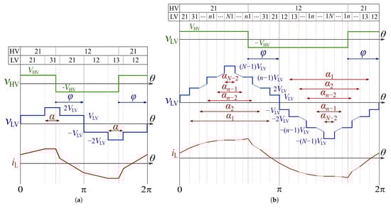
Figure 5.
Voltages vHV and vLV and current iL. The switching states are represented at the top of each subfigure as (xy), where x,y indicate the DC-link node to which legs 1 and 2 of the corresponding converter side (HV and LV) are connected, respectively. (a) For the 2L-3L NPC DAB converter. (b) For the 2L-NL NPC DAB converter.
Figure 6a illustrates along with the converter’s 3L-side switching pattern. The fundamental component of the inductor current is divided into a component in phase with , i.e., , and a component in quadrature with , i.e., . To visualize the current distribution among the DC-link nodes, the red areas in Figure 6a depict the charge injected (+)/drawn (−) by and by into/from node , while the green areas depict the charge injected (+)/drawn (−) into/from node . Due to the quarter-wave symmetry of the AC voltage waveform, only the in-phase component transfers power to the DC-link nodes, whereas does not contribute to power injection, as its positive and negative areas cancel out over a switching period, and it is disregarded in the analysis. The LV-side switching pattern ensures that the average currents injected by into and are positive, which are expressed as
where is the amplitude of , and is the transformer’s turns ratio, as defined in Figure 2c. The angle controls the currents’ ratio , while controls their total sum .
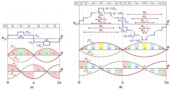
Figure 6.
Voltage vLV and currents iL,1p and iL,1q. (a) For the 2L-3L NPC DAB converter. The red and green areas depict the charges injected (+) or drawn (−) into/from nodes 2LV and 3LV, respectively. (b) For the 2L-NL NPC DAB converter. The yellow, blue, green, and red areas depict the charges injected (+) or drawn (−) into/from nodes NLV, nLV, 3LV, and 2LV, respectively.
2.3. Modulation Strategy for the Multiport 2L-NL NPC DAB Converter
Building upon the 2L-3L NPC DAB strategy, a modulation and switching strategy for the generalized 2L-NL NPC DAB converter is proposed. The converter features battery modules and N nodes in its LV-side DC link. Figure 5b presents the waveforms for , , and , as well as the converter’s HV-side and LV-side switching patterns. As with the 2L-3L converter, is a two-level square waveform. The secondary-side voltage is a stepped waveform featuring levels. The modulation uses DoFs: the phase shift, , and the modulation angles, , which control the dwell time at each voltage level.
Figure 6b illustrates along with the converter’s NL-side switching pattern. As with the 2L-3L converter, features quarter-wave symmetry; thus, only transfers power to the DC-link nodes. Figure 6b depicts the charge injected into nodes to . The LV-side switching pattern ensures that the average current injected by into node n is positive, which is expressed as
The proposed modulation strategy thus allows control of the current injected into each DC-link node by properly adjusting the modulation angles, .
2.4. Assessment of Conduction Losses for the Proposed Modulation Strategy
The modulation strategy proposed for the generalized 2L-NL NPC DAB converter eliminates zero-voltage dwell times in and , thereby maximizing the amplitude of their fundamental components, which directly impacts the conduction losses of the converter. In a DAB converter, the root-mean-square (RMS) value of the current flowing through the HF inductor, , is commonly used as a figure of merit for the converter’s conduction losses [28]. In the APM, minimizing conduction losses is a priority due to the LV side’s high operating currents resulting from the low operating voltage of the auxiliary system.
To illustrate the RMS current minimization, the duty ratio is introduced. This parameter, expressed in p.u., defines the zero-voltage dwell time of over a switching period. In the proposed modulation strategy, the modulation angles are defined such that . However, it is possible to implement a modulation strategy with the same DoFs while fixing .
Figure 7a,b show the HF link AC voltage and current waveforms for a multiport 2L-3L NPC DAB converter at the nominal operating point of the converter () for and , respectively. Figure 7c presents the value of across the full operating range of the converter (, ) for , , and . Comparing Figure 7a,b shows that the current amplitude is lower when .
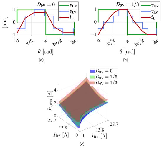
Figure 7.
(a) AC voltage and current waveforms at the nominal operating point of the converter () for . (b) AC voltage and current waveforms at the nominal operating point of the converter () for . (c) Value of across the full operating range of the converter (, , , , ).
The results in Figure 7c show that the minimum is achieved when across the entire operating range, and that its value increases with , reaching a maximum for all combinations of when . Therefore, fixing results in a minimum inductor RMS current, thereby minimizing conduction losses in the converter. In this case, the amplitude of the fundamental component of is reduced, requiring a higher value of to inject the same amount of current into the LV DC-link nodes. Consequently, increases.
3. Generalized Control Strategy
3.1. Derivation of the SoC Expression for LV Battery Modules
To design an effective control strategy for the multiport 2L-NL NPC DAB converter, it is necessary to derive the expression for the variables to be controlled, i.e., the SoC of the LV battery modules connected to the NL-side DC link, as a function of the DoFs of the converter, i.e., the modulation angles .
The SoC of the nth battery module at a given instant is expressed as
where , and C is the capacity of each battery module. From Equations (3) and (8), the current in the battery modules is
The expression for is derived by analyzing the converter considering only the fundamental components of the HF voltages, and . Figure 8 depicts a simplified representation of the converter’s HF link, where is the LV-side AC voltage, referred to the HV side.
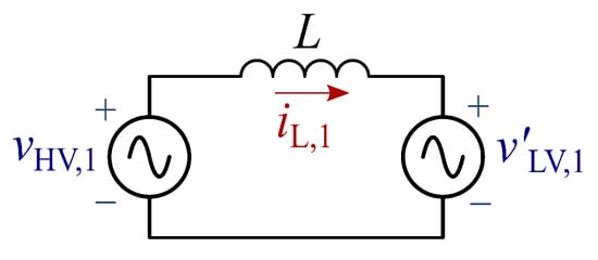
Figure 8.
Fundamental model of the converter’s HF link.
The power transferred by the converter is
where and are the amplitudes of the AC voltages, L is the series inductance, and f is the converter switching frequency. Alternatively, can be expressed as
3.2. Closed-Loop Control
Equation (15) illustrates the relation between the controlled variables ,, …, , and the modulation angles . The value of only depends on , whereas the values of to depend on both and their corresponding angles, to . Thus, ,, …, are regulated by adjusting the value of the modulation angles , , respectively.
Figure 9 depicts the proposed generalized closed-loop control strategy for the multiport 2L-NL NPC DAB converter. The output variables to are controlled by adjusting the value of the control variables, i.e., the modulation angles to . The error between the reference and measured values for the output variables ( and , respectively) is the input of PI compensators, whose outputs, to , are bounded, obtaining the values of the modulation angles ( to ).
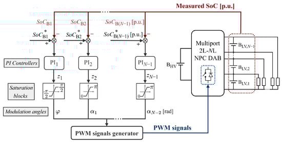
Figure 9.
Generalized closed-loop control scheme.
4. Generalized Decoupled Control Strategy
In the control system depicted in Figure 9, each output variable, to , is controlled by adjusting the value of a single modulation angle, to .
However, a variation in simultaneously affects all output variables. If deviates from its reference, the controller adjusts such that to properly charge/discharge and correct the SoC error. While only depends on , currents to depend on both and their respective angles, to (Equation (14)). Consequently, when the controller adjusts to correct an deviation, to are perturbed, resulting in modules to being discharged, thereby causing the output variables to to deviate from their references. Therefore, a coupling exists between the control loop and the rest of the battery modules’ SoC control loops.
To mitigate this coupling, let us define a decoupling strategy based on a decoupling matrix. To do so, the plant is linearized, assuming that the converter operates at an equilibrium operating point.
Around a given equilibrium point, i.e., in steady-state operation, the modulation angles are expressed as
where are the values of the angles at equilibrium, and represent small variations from equilibrium.
Furthermore, the current in the nth battery module can be linearized as
where is the equilibrium value and
In steady state, is constant, i.e., . Then, , and the linear expressions for are
From Equations (15) and (19), the variations in the control output variables are then expressed in the Laplace domain as
Thus, the plant transfer function matrix can be defined as
where and is the plant coupling matrix, derived from Equation (20) and expressed as
The plant can then be decoupled by multiplying the compensators’ output variables, , by the inverse of the plant coupling matrix, [29]. Then, the decoupled plant transfer function for the generalized decoupled control strategy is
where the generalized expression of is
Figure 10 illustrates the generalized decoupled closed-loop control scheme for the multiport 2L-NL NPC DAB converter. The output variables, to , are controlled by adjusting the value of the modulation angles, to . The errors between the reference and measured values of the output variables are the inputs to PI compensators. The outputs of these compensators ( to ) are then multiplied by the decoupling matrix , and the resulting vector is added to the vector of the modulation angles at equilibrium, thereby obtaining the modulation angles ( to ), whose values are bounded to for and for to . The components of are expressed as functions of the equilibrium angles, . The equilibrium angles are obtained by applying a low-pass filter to the effective modulation angles. From Equation (24), some components of the matrix become undefined for , , and . To avoid these singularities, the equilibrium angles are bounded for the computation of such that and .
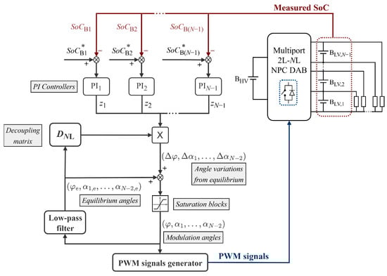
Figure 10.
Generalized decoupled closed-loop control scheme.
5. Results
This section presents the results obtained to validate the proposed control strategy. Hardware-in-the-loop (HIL) tests were performed for the 2L-3L NPC DAB and 2L-4L NPC DAB converters. In addition, MATLAB/Simulink simulations were performed for the 2L-5L NPC DAB converter to validate its scalability. Finally, a simulation-based sensitivity analysis was performed using MATLAB/Simulink to evaluate the control robustness under disturbances in the battery current measurements and a capacity reduction in the LV battery modules.
5.1. Hardware-in-the-Loop Tests
Hardware-in-the-loop (HIL) tests were performed to validate the proposed control strategy. Figure 11 illustrates the experimental setup for the HIL tests. The electrical system was simulated in a HIL 404 real-time simulator by Typhoon HIL with a fixed time step of 250 ns. The HV and LV battery modules were modeled as ideal voltage sources. The control loop and the PWM modulator were executed in real time in the digital signal processor (DSP) and the field-programmable gate array (FPGA) of a dSPACE MicroLabBox platform, respectively. The DSP and the FPGA operated with a fixed time step of 250 ns and 10 ns, respectively. The HIL simulator included short-circuit detection. Therefore, a dead time of 300 ns was included in the PWM signals generated by the FPGA during switching transitions.
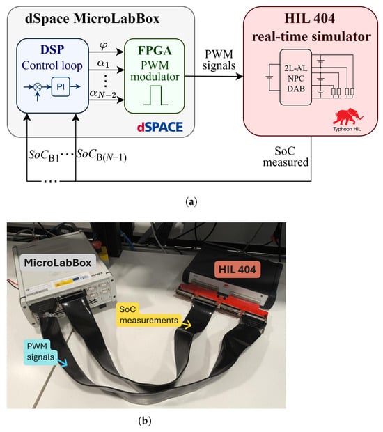
Figure 11.
Connection of the dSPACE MicroLabBox and the HIL 404 real-time simulator for the HIL tests. (a) Diagram illustrating the connection and the signal exchange between platforms. (b) Picture of the experimental setup.
This section presents the results obtained for the multiport 2L-3L NPC DAB converter and for the multiport 2L-4L NPC DAB converter. The non-decoupled control strategy (Section 3) and the decoupled control strategy (Section 4) were evaluated for both converters. Two types of tests were performed to compare the performance of the non-decoupled and decoupled control strategies. First, the SoC reference values of the LV battery modules, , were modified, with the converter operating at its nominal operating point, i.e., with the auxiliary loads sinking their maximum current (Equation (5)). In the second test, the current sunk by the auxiliary loads was varied, thereby modifying the operating point of the converter.
5.1.1. Multiport 2L-3L NPC DAB Converter
The electrical parameters of the multiport 2L-3L NPC DAB converter, the current sunk by the auxiliary loads at the nominal operating point, and the parameters of the PI controllers used in both the non-decoupled and decoupled control strategies are summarized in Table 1.

Table 1.
Electrical parameters of the 2L-3L NPC DAB converter, the nominal current sunk by the auxiliary loads, and the parameters of the PI controllers for the HIL tests.
Figure 12 shows the response of the system to variations in the SoC reference values of the LV battery modules, and . The converter operates at its nominal operating point, i.e., the auxiliary loads sink 27.7 A.
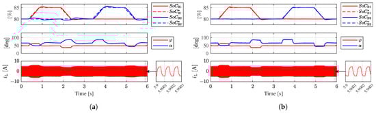
Figure 12.
HIL test results for the 2L-3L case. System responses to variations in the SoC reference values. (a) Using the non-decoupled closed-loop control strategy. (b) Using the decoupled closed-loop control strategy.
Figure 12a shows the results of applying the generalized non-decoupled closed-loop control strategy. At time = 0.35 s, increases from 80% to 85% in 0.5 s. Then, the control correspondingly increases from 47° to 62° during the transient to ensure that the measured tracks its reference value. Conversely, when is reduced back to 80%, decreases from 47° to 37°. However, the value of is also affected by the variations in due to the coupling of regulation to the regulation of the other modules SoCs, as described in Section 4. When increases/decreases, the total current injected by the converter into the LV DC-link nodes increases/decreases. Therefore, the current flowing through all the battery modules becomes positive/negative, increasing/decreasing their SoC. Then, when is modified by the closed-loop control strategy to correct an error in , deviates from its reference value. The value of is then adjusted by the control loop to compensate for the error between and .
On the other hand, when increases/decreases (at ), the control loop correspondingly increases/decreases to properly adjust , while the measured remains stable at its reference value, as its value does not depend on .
Figure 12b shows the response of the system when the decoupled closed-loop control strategy is used. The coupling effect is mitigated due to the use of the decoupling matrix, with remaining stable around its reference value when varies. Furthermore, the use of the decoupled control loop yields better and reference tracking. After a variation in , the measured SoC exhibits a peak overshoot of 0.5%, similar to the peak observed in when the non-decoupled control strategy was used (Figure 12a). After the reference transitions, the values of and stabilize around the new reference values in less than 0.3 s, demonstrating better dynamic performance than the non-decoupled control strategy.
Figure 13 shows the response of the system to a 36% (10 A) drop in the current sunk by the auxiliary loads from its nominal operating point, while and remain constant at 80%.
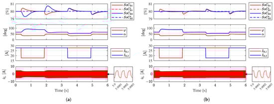
Figure 13.
HIL tests results for the 2L-3L case. System responses to variations in the current sunk by the LV loads. (a) Using the non-decoupled closed-loop control strategy. (b) Using the decoupled closed-loop control strategy.
Figure 13a shows the results for the non-decoupled closed-loop control strategy. At time = 0.35 s, drops from 27.7 A to 17.7 A. In this situation, before the closed-loop control adjusts the modulation angles to the new operating point. Then, temporarily absorbs the excess current injected by the converter into node , consequently increasing . The closed-loop control then decreases the value of from 47° to 36° to correct the error. Due to the plant coupling, the decrease in results in a reduction in , which is corrected by adjusting the value of . Conversely, when increases back to 27.7 A, the control loop increases to adjust the operating point of the converter, resulting in an undesired increase in , which is corrected by adjusting the value of .
On the other hand, when drops to 17.7 A, before the closed-loop control adjusts the modulation angles to the new operating point. Thus, and temporarily absorb the excess current injected by the converter into node , increasing their SoCs. The closed-loop control then modifies and to correct the difference between their reference values and measured SoCs, adjusting to the new converter operating point. Conversely, when increases back to 27.7 A, the values of and temporarily decrease before the modulation angles are adjusted to the new operating point.
Figure 13b shows the response of the system when the decoupled closed-loop control strategy is used. As with the SoC variation test, the coupling effect when stepping is mitigated. On the other hand, the response of the system to the variation in is similar to that observed with the non-decoupled control strategy. Across all transitions, the measured SoCs for all battery modules stabilize around their reference values in less than 0.5 s.
In summary, the results confirm that the proposed non-decoupled closed-loop control strategy effectively maintains the SoC of the LV battery modules at their reference values for the multiport 2L-3L NPC DAB converter, adjusting the modulation angles to correct any deviations due to changes in the operating point of the converter. Moreover, the proposed decoupling strategy enhances the performance of the control strategy, resulting in the mitigation of the coupling of regulation to regulation.
5.1.2. Multiport 2L-4L NPC DAB Converter Results
The electrical parameters of the multiport 2L-4L NPC DAB converter, the current sunk by the auxiliary loads at the nominal operating point, and the parameters of the PI controllers used in both the non-decoupled and decoupled control strategies are summarized in Table 2.
Table 2.
Electrical parameters of the 2L-4L NPC DAB converter, the nominal current sunk by the auxiliary loads, and the parameters of the PI controllers for the HIL tests.
Figure 14 shows the responses of the system to variations in the SoC reference values of the LV battery modules, to .
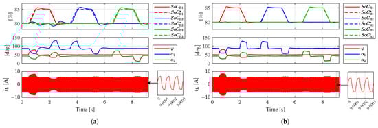
Figure 14.
HIL test results for the 2L-4L case. System responses to variations in the SoC reference values. (a) Using the non-decoupled closed-loop control strategy. (b) Using the decoupled closed-loop control strategy.
Figure 14a shows the results for the non-decoupled closed-loop control strategy. At time = 0.5 s, increases from 80% to 85% in 0.5 s. Then, the closed-loop control increases from 50° to 80° to ensure that the measured tracks its reference value. When is reduced back to 80%, is decreased to 34°. As with the 2L-3L converter, the values of and are affected by the variations of due to the described control coupling. Then, the closed-loop control adjusts and to stabilize and at their reference values. When or increases/decreases, the closed-loop control increases/decreases their corresponding angle ( for , for ) to ensure that and track their references. As with the 2L-3L DAB converter, the SoCs of the other LV battery modules remain stable around their reference.
Figure 14b shows the response of the system when the decoupled closed-loop control strategy is used. As with the 2L-3L converter, the coupling of regulation to the regulation of the other modules’ SoCs is mitigated due to the use of the decoupling matrix, with and remaining stable around their reference values, and the use of the decoupled control loop yields better , and reference tracking. As with the 2L-3L configuration, after varying , presents a peak overshoot of 0.5%, similar to the peak observed in when the non-decoupled control strategy was used (Figure 14a). After the reference transitions, the values of to stabilize around the new references in less than 0.3 s, demonstrating better dynamic performance than the non-decoupled control strategy.
Figure 15 shows the response of the system to a 36% (5 A) drop in the current sunk by the auxiliary loads from its nominal operating point, while , , and remain constant at 80%.
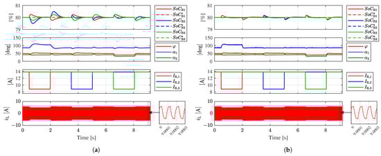
Figure 15.
HIL test results for the 2L-4L case. System responses to variations in the current sunk by the LV loads. (a) Using the non-decoupled closed-loop control strategy. (b) Using the decoupled closed-loop control strategy.
In Figure 15a, the generalized non-decoupled closed-loop control is tested. At time = 0.5 s, steps down from 13.8 A to 8.8 A. Similarly to the 2L-3L case, temporarily absorbs the excess current injected by the converter into node , causing to rise. Then, the closed-loop control strategy decreases the value of from 50° to 40° to correct the error and adjust the operating point of the converter. Conversely, when increases back to 13.8 A, the control loop increases . Increasing/reducing results in increases/reductions in and due to coupling. This effect is compensated for by the closed-loop control strategy through the adjustment of and .
When drops to 8.8 A, and absorb the excess current injected by the converter into node , thereby raising their SoC values. Then, the closed-loop control strategy reduces the values of and . However, the coupling effect leads to a reduction in ; thus, the closed-loop control strategy adjusts to correct the deviation.
Finally, variations in cause a positive/negative current to flow through all LV battery modules, thereby increasing/decreasing their SoCs. Then, the control loop strategy modifies , , and to correct the error between the measured and reference SoCs and adjust to the new operating point.
Figure 15b shows the response of the system when the decoupled closed-loop control strategy is used. Notably, the coupling effect when or decreases/increases is mitigated due to the use of the decoupling matrix. Indeed, when varies, the values of and remain stable around their reference values, and variations in produce a negligible disturbance on the value of . Furthermore, when increases/decreases, the modules’ SoCs decrease/increase at a similar pace, as expected in a fully decoupled control scenario. Across all transitions, the measured SoCs for all battery modules stabilize around their reference values in less than 0.5 s.
Again, the results confirm that the proposed control strategy effectively maintains the SoCs of the LV battery modules at their reference values for the multiport 2L-4L NPC DAB converter, with the decoupling strategy successfully mitigating the coupling effect and improving the regulation of the SoC during the and load transients.
5.2. Simulation Results for the 2L-5L NPC DAB Converter
To assess the scalability of the proposed control strategy, a simulation was performed using MATLAB/Simulink for the 2L–5L NPC DAB converter using the decoupled closed-loop control strategy. Computer-based simulations were chosen instead of HIL tests due to the inability to implement the 2L-5L topology in the available HIL equipment (see Section 5.1). The electrical parameters of the converter, the current sunk by the auxiliary loads at the nominal operating point, and the parameters of the PI controllers are summarized in Table 3.
Table 3.
Electrical parameters of the 2L-5L NPC DAB converter, the nominal current sunk by the auxiliary loads, and the parameters of the PI controllers for the MATLAB/Simulink simulation.
Figure 16 shows the response of the system to a 5% variation over 0.7 s in the SoC reference values of the LV battery modules, to . The converter operates at its nominal operating point. As with the 2L-3L DAB converter, the SoCs of all LV battery modules remain stable around their reference values both in steady-state operation and under variations in the reference SoCs. When the reference SoCs increase or decrease, the measured SoCs for all battery modules stabilize around their respective reference values within 0.5 s, showing a fast dynamic response to variations. Moreover, the coupling of regulation to the regulation of the other modules’ SoCs is clearly mitigated, with , , and remaining stable around their reference values when increases/decreases.
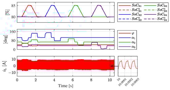
Figure 16.
Simulation results for the 2L-5L case. System response to variations in the SoC reference values.
5.3. Simulation-Based Sensitivity Analysis of the Decoupled Control Strategy
To further validate the robustness of the proposed decoupled control strategy, a software-based sensitivity analysis was performed using MATLAB/Simulink models.
This study focused on the multiport 2L–3L NPC DAB converter model and evaluated the impact of three non-idealities on the system’s response: an HF disturbance injected into the measurement of , a low-frequency (LF) disturbance injected into the measurement of , and a 10% reduction in the capacity of the battery modules from 83 Ah to 74.7 Ah, emulating degradation due to aging.
The electrical parameters of the 2L-3L NPC DAB converter, the nominal current sunk by the auxiliary loads, and the parameters of the PI controllers used in the simulations were the same as those employed for the HIL tests and are shown in Table 1.
5.3.1. High-Frequency Disturbance Injected into the Measurement of
Figure 17 shows the response of the system to variations in the SoC reference values of the LV battery modules, (Figure 17a) and (Figure 17b), under an HF disturbance injected into the measurement of . A disturbance consisting of a sinusoidal waveform with 1 A amplitude and 10 kHz frequency was considered.
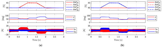
Figure 17.
Simulation results under an HF disturbance injected into the measurement of . (a) Variation in . (b) Variation in .
As observed in the results, the modulation angles remain unaffected by the injection of the HF disturbance into . The variations in the battery modules’ SoCs are estimated by integrating and . Then, due to their alternating nature, HF signals tend to cancel out over short time intervals when integrated, and the integration process acts as a low-pass filter. Therefore, the control outputs and remain unaffected, and the control loop is robust against HF disturbances injected into the battery current measurements.
5.3.2. Low-Frequency Disturbance Injected into the Measurement of
Figure 18 shows the response of the system to variations in the SoC reference values of the LV battery modules, (Figure 18a) and (Figure 18b), under an LF disturbance injected into the measurement of . A disturbance consisting of a sinusoidal waveform with 1 A amplitude and 50 Hz frequency was injected.
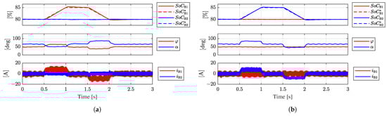
Figure 18.
Simulation results under an LF disturbance into the measurement of . (a) Variation in . (b) Variation in .
The variation in the battery modules’ SoCs is proportional to the integral of the measured current through the battery module (Equation (9)), with the integration process acting as a low-pass filter. Consequently, LF disturbances directly affect the estimation of and , and impact the control outputs and . As observed in the results, angle exhibits a steady-state oscillation with a peak amplitude of 3.4° (Figure 18b, time = 2.5 s), and angle oscillates in steady-state operation with a maximum amplitude of 1.8° (Figure 18b, time = 2.5 s). Despite these oscillations, the control loop is able to maintain the stability of and around their reference values, effectively adjusting the average value of the modulation angles to track the reference SoC values.
The simulation results confirm that a severe LF disturbance injected into the battery modules’ current measurements affects the control output, generating LF oscillations in and . Nevertheless, the decoupled control strategy successfully maintains the stability of and around their reference values during steady-state operation and under variations in and .
5.3.3. Reduction in the Capacity of the Battery Modules
Figure 19 shows the response of the system to variations in the SoC reference values of the LV battery modules, (Figure 19a) and (Figure 19b), under a 10% reduction in the capacity of the battery modules from 83 Ah to 74.7 Ah.
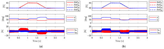
Figure 19.
Simulation results under an 10% reduction in the battery modules capacity. (a) Variation in . (b) Variation in .
The results show that the control system performance is not affected by the capacity reduction in the battery modules. Both and remain stable around their reference values in steady-state operation and track their reference values when these are increased/decreased. The modulation angles and remain stable and do not present oscillations in steady-state operation. Moreover, the coupling of regulation to the regulation of the other modules’ SoCs remains mitigated. Therefore, the results show that the decoupled control loop strategy is robust to moderate variations in the capacity of the battery modules caused by degradation.
6. Discussion
This paper proposes a single-stage multiport APM capable of supplying multiple groups of auxiliary loads, each operating at a different voltage level. To achieve this, LV battery modules are connected in series and powered through a 2L-NL NPC DAB converter. As a result, DC ports are obtained from the nodes of the DC link formed by the series-connected battery modules, allowing the feeding of groups of loads, each connected to its optimal operating voltage.
A generalized modulation strategy for the 2L-NL NPC DAB converter using DoF () is employed to compensate for the unbalanced LV battery modules’ currents caused by the load connections to the DC ports, thereby keeping the modules’ SoCs balanced. The proposed modulation strategy minimizes the inductor RMS current and therefore the conduction losses in the converter.
A generalized closed-loop control strategy regulating the SoC of the LV battery modules is proposed and validated through HIL tests, under variations in the modules’ reference SoCs and variations in the power sunk by the loads. A coupling of the bottom-module SoC control to the rest of the modules’ SoCs is identified, and a decoupled closed-loop control strategy, based on the use of a decoupling matrix, is proposed to mitigate the coupling between the output variables of the closed-loop control. Its performance is validated through HIL tests and MATLAB/Simulink simulations, showing greater SoC regulation performance than the non-decoupled control strategy, as well as a simulation-based sensitivity analysis.
The proposed connection aligns with ongoing research in the field aimed at obtaining a multiple-voltage architecture in the AS of the EVs [11,12,13,14,15,16,17,18,19,20,21,22]. Table 4 presents a comparison, in terms of required components and converter modularity, between the proposed 2L-NL NPC DAB converter in its 2L-3L implementation and two alternative three-port converters for the APM application: the TAB presented in [11] and the three-port resonant DC-DC converter presented in [13]. All three topologies can be employed in the APM and feature an HF link interfacing their HV and LV sides. The TAB provides full isolation between all DC ports, whereas the 2L-3L NPC DAB converter and the resonant DC-DC converter offer isolation only between the converter’s HV and LV sides, which is sufficient for the APM use case.
Table 4.
Comparison between the multiport 2L-3L NPC DAB converter, the TAB, and the three-port resonant DC-DC converter.
On the LV side, all three topologies present two DC ports. For the TAB and the resonant DC-DC converter topologies, a total of eight LV switches is required, the same as in the 2L-3L NPC DAB converter when using NPC legs, and four fewer than in the 2L-3L NPC DAB converter when using ANPC legs. The TAB uses switches with different voltage ratings in each LV bridge, and in the resonant DC-DC converter, all LV switches share the same voltage rating, which is determined by the higher-voltage DC port. Conversely, in the 2L-3L NPC DAB converter, all the LV switches feature the same voltage rating, defined by the lower-voltage DC port. For the same DC-port voltage, this allows the use of lower-voltage-rated devices with better performance, enhancing the overall conversion efficiency. Moreover, the TAB and the resonant DC-DC converter require more passive elements than the proposed 2L-3L NPC DAB converter, which negatively impacts converter power density and efficiency. Finally, the modular nature of the 2L-3L NPC DAB converter allows scaling the number of DC ports while using the same voltage-rated switches and without requiring new passive elements in the converter. This is a key advantage over other multiport topologies. The resonant converter in [13] cannot be directly scaled to obtain more DC ports without structural modifications. The TAB can be generalized to obtain the multi-active-bridge converter (MAB) [30]; however, adding a DC port requires four additional switches (rated at the DC-port voltage) and an additional transformer winding and inductor, impacting efficiency and power density. Moreover, as the number of ports increases in the MAB, its control becomes more complex due to the coupling between the power transfer between the DC ports.
Further work could explore an optimization of the converter’s electrical parameters, such as the series inductance or the switching frequency, to obtain a converter design with minimum conduction and switching losses and high power density. Moreover, performance optimization could be explored by introducing additional DoFs to the proposed modulation, such as new modulation angles controlled by an advanced control strategy capable of optimizing their values for different operating points of the converter.
Author Contributions
Conceptualization, methodology, investigation, validation: O.E.-M., A.F.-M. and J.N.-A.; formal analysis: O.E.-M.; resources: A.F.-M. and J.N.-A.; writing—original draft preparation and review and editing: O.E.-M., A.F.-M. and J.N.-A.; supervision: A.F.-M., J.N.-A., and S.B.-M.; project administration and funding acquisition: A.F.-M. and S.B.-M. All authors have read and agreed to the published version of the manuscript.
Funding
This work was funded by the European Union’s Horizon Europe Research and Innovation Program under grant agreement no. 101056781. The views and opinions expressed are, however, those of the author(s) only and do not necessarily reflect those of the European Union or CINEA. Neither the European Union nor the granting authority can be held responsible for them.
Data Availability Statement
Data are within the article.
Conflicts of Interest
The authors declare no conflicts of interest.
References
- Speizer, S.; Fuhrman, J.; Lopez, L.A.; George, M.; Kyle, P.; Monteith, S.; McJeon, H. Integrated assessment modeling of a zero-emissions global transportation sector. Nat. Commun. 2024, 15, 4439. [Google Scholar] [CrossRef] [PubMed]
- Global CO2 Emissions from Transport by Subsector in the Net Zero Scenario, 2000–2030. Available online: https://www.iea.org/data-and-statistics/charts/global-co2-emissions-from-transport-by-subsector-2000-2030 (accessed on 2 May 2025).
- European Commission: Directorate-General for Communication. The European Green Deal; Publications Office: Luxembourg, 2020. [Google Scholar] [CrossRef]
- Wang, C.; Zheng, P.; Bauman, J. A review of electric vehicle auxiliary power modules: Challenges, topologies, and future trends. IEEE Trans. Power Electron. 2023, 38, 11233–11244. [Google Scholar] [CrossRef]
- De Doncker, R.; Divan, D.; Kheraluwala, M. A three-phase soft-switched high-power-density DC/DC converter for high-power applications. IEEE Trans. Ind. Appl. 1991, 27, 63–73. [Google Scholar] [CrossRef]
- Hou, R.; Magne, P.; Bilgin, B.; Emadi, A. A topological evaluation of isolated DC/DC converters for Auxiliary Power Modules in Electrified Vehicle applications. In Proceedings of the 2015 IEEE Applied Power Electronics Conference and Exposition (APEC), Charlotte, NC, USA, 15–19 March 2015; pp. 1360–1366. [Google Scholar] [CrossRef]
- Walter, J.; De Doncker, R. High-power galvanically isolated DC/DC converter topology for future automobiles. In Proceedings of the IEEE 34th Annual Conference on Power Electronics Specialist, 2003. PESC ’03, Acapulco, Mexico, 15–19 June 2003; Volume 1, pp. 27–32. [Google Scholar] [CrossRef]
- Krismer, F.; Kolar, J.W. Accurate power loss model derivation of a high-current dual active bridge converter for an automotive application. IEEE Trans. Ind. Electron. 2010, 57, 881–891. [Google Scholar] [CrossRef]
- Li, N.; Zhang, C.; Liu, Y.; Zhuo, C.; Liu, M.; Yang, J.; Zhang, Y. Single-Degree-of-Freedom Hybrid Modulation Strategy and Light-Load Efficiency Optimization for Dual-Active-Bridge Converter. IEEE J. Emerg. Sel. Top. Power Electron. 2024, 12, 3936–3947. [Google Scholar] [CrossRef]
- Kotb, R.; Chakraborty, S.; Tran, D.-D.; Abramushkina, E.; El Baghdadi, M.; Hegazy, O. Power electronics converters for electric vehicle auxiliaries: State of the art and future trends. Energies 2023, 16, 1753. [Google Scholar] [CrossRef]
- Zhao, C.; Round, S.D.; Kolar, J.W. An Isolated Three-Port Bidirectional DC-DC Converter with Decoupled Power Flow Management. IEEE Trans. Power Electron. 2008, 23, 2443–2453. [Google Scholar] [CrossRef]
- Keshmiri, N.; Mudiyanselage, G.A.; Chakkalakkal, S.; Kozielski, K.; Pietrini, G.; Emadi, A. Design and control methodology of a threeport resonant converter for electric vehicles. IEEE Open J. Ind. Electron. Soc. 2022, 3, 650–662. [Google Scholar] [CrossRef]
- Do, N.-Q.; Lee, C.; Kim, J.; Kieu, H.-P.; Choi, S. 800V/48V/12V 6kW resonant dc-dc converter with dual transformers for Electric Vehicles. In Proceedings of the 2024 IEEE 10th International Power Electronics and Motion Control Conference (IPEMC2024-ECCE Asia), Chengdu, China, 17–20 May 2024; pp. 1959–1963. [Google Scholar] [CrossRef]
- Kotb, R.; Chakraborty, S.; Hegazy, O. Efficient and Bidirectional Cascaded Auxiliary Power Module Design for Electric Trucks Using Hybrid Si, SiC, and GaN Technologies. In Proceedings of the 2024 Third International Conference on Sustainable Mobility Applications, Renewables and Technology (SMART), Dubai, United Arab Emirates, 22–24 November 2024; pp. 1–9. [Google Scholar] [CrossRef]
- Kieu, H.-P.; Do, N.-Q.; Choi, S. A New Bidirectional Three Port DC-DC Converter for Dual Auxiliary Voltage in EV Application. In Proceedings of the 2024 IEEE 10th International Power Electronics and Motion Control Conference (IPEMC2024-ECCE Asia), Chengdu, China, 17–20 May 2024; pp. 1870–1874. [Google Scholar] [CrossRef]
- Itoh, K.; Inoue, S.; Ishigaki, M.; Sugiyama, T.; Sugai, M. Loss estimation of an isolated three-port DC-DC converter for automotive applications. In Proceedings of the 2015 IEEE Energy Conversion Congress and Exposition (ECCE), Montreal, QC, Canada, 20–24 September 2015; pp. 3667–3673. [Google Scholar] [CrossRef]
- Vahid, S.; Zolfi, P.; Land, J.C.; EL-Refaie, A.M. An Isolated Step-Down Multi-Port DC-DC Power Converter for Electric Refrigerated Vehicles Auxiliary Power Unit System. IEEE Trans. Ind. Appl. 2024, 60, 730–744. [Google Scholar] [CrossRef]
- Kieu, H.-P.; Do, N.-Q.; Choi, S. Dual Floating Based Three Port DC-DC Converter for EV-APM. IEEE Trans. Power Electron. 2025, 40, 4268–4278. [Google Scholar] [CrossRef]
- Ishigaki, M.; Ito, K.; Tomura, S.; Umeno, T. A new isolated multiport converter using interleaving and magnetic coupling inductor technologies. In Proceedings of the 2013 Twenty-Eighth Annual IEEE Applied Power Electronics Conference and Exposition (APEC), Long Beach, CA, USA, 17–21 March 2013; pp. 1068–1074. [Google Scholar] [CrossRef]
- Inoue, S.; Itoh, K.; Ishigaki, M.; Sugiyama, T. Magnetically integrated isolated bidirectional three-port DC-DC converter. In Proceedings of the 2017 19th European Conference on Power Electronics and Applications (EPE’17 ECCE Europe), Warsaw, Poland, 11–14 September 2017; pp. P.1–P.10. [Google Scholar] [CrossRef]
- Li, Y.; Wang, Y.; Guan, Y.; Xu, D. Design and Optimization of High-Gain Bidirectional DC–DC Converter for Electric Vehicles. IEEE Trans. Power Electron. 2023, 38, 11221–11232. [Google Scholar] [CrossRef]
- Uno, M.; Sato, M.; Tada, Y.; Iyasu, S.; Kobayashi, N.; Hayashi, Y. Partially Isolated Multiport Converter with Automatic Current Balancing Interleaved PWM Converter and Improved Transformer Utilization for EV Batteries. IEEE Trans. Transp. Electrif. 2023, 9, 1273–1288. [Google Scholar] [CrossRef]
- Filba-Martinez, A.; Busquets-Monge, S.; Bordonau, J. Modulation and Capacitor Voltage Balancing Control of Multilevel NPC Dual Active Bridge DC–DC Converters. IEEE Trans. Ind. Electron. 2020, 67, 2499–2510. [Google Scholar] [CrossRef]
- Lee, J.-y.; Choi, H.-j.; Jung, J.-h. Three level NPC dual active bridge capacitor voltage balancing switching modulation. In Proceedings of the 2017 IEEE International Telecommunications Energy Conference (INTELEC), Broadbeach, QLD, Australia, 22–26 October 2017; pp. 438–443. [Google Scholar] [CrossRef]
- Lee, J.-Y.; Cho, Y.-P.; Jung, J.-H. Single-Stage Voltage Balancer With High-Frequency Isolation for Bipolar LVDC Distribution System. IEEE Trans. Ind. Electron. 2020, 67, 3596–3606. [Google Scholar] [CrossRef]
- Kolahian, P.; Tarzamni, H.; Nikafrooz, A.; Hamzeh, M. A Multi-port DC-DC Converter for Bipolar MVDC Micro-grid Applications. IET Power Electron. 2019, 12, 1841–1849. [Google Scholar] [CrossRef]
- Busquets-Monge, S.; Webster, J.G. Neutral-Point-Clamped DC–AC Power Converters. In Wiley Encyclopedia of Electrical and Electronics Engineering; John Wiley & Sons, Inc.: Hoboken, NJ, USA, 2018; pp. 1–20. [Google Scholar] [CrossRef]
- Borrell-Pons, E.; Esquius-Mas, O.; Filba-Martinez, A.; Trilla, L. A Novel Mathematical Approach for Inductor-Current Expressions Definition in Multilevel Dual-Active-Bridge Converters. Electronics 2024, 13, 4476. [Google Scholar] [CrossRef]
- Busquets-Monge, S.; Griñó, R.; Nicolas-Apruzzese, J.; Bordonau, J. Decoupled DC-Link Capacitor Voltage Control of DC–AC Multilevel Multileg Converters. IEEE Trans. Ind. Electron. 2016, 63, 1344–1349. [Google Scholar] [CrossRef]
- Chen, Y.; Wang, P.; Li, H.; Chen, M. Power Flow Control in Multi-Active-Bridge Converters: Theories and Applications. In Proceedings of the 2019 Applied Power Electronics Conference and Exposition (APEC), Anaheim, CA, USA, 17–21 March 2019; pp. 1500–1507. [Google Scholar] [CrossRef]
Disclaimer/Publisher’s Note: The statements, opinions and data contained in all publications are solely those of the individual author(s) and contributor(s) and not of MDPI and/or the editor(s). MDPI and/or the editor(s) disclaim responsibility for any injury to people or property resulting from any ideas, methods, instructions or products referred to in the content. |
© 2025 by the authors. Licensee MDPI, Basel, Switzerland. This article is an open access article distributed under the terms and conditions of the Creative Commons Attribution (CC BY) license (https://creativecommons.org/licenses/by/4.0/).