Article

A Power Boosting Method for Wireless Power Transfer Systems Based on a Multilevel Inverter and Dual-Resonant Network

1
College of Automation, Wuxi University, Wuxi 214105, China
2
School of Automation, Nanjing University of Information Science & Technology, Nanjing 210044, China
*
Author to whom correspondence should be addressed.
Electronics 2024, 13(20), 4066; https://doi.org/10.3390/electronics13204066
Submission received: 19 September 2024 / Revised: 10 October 2024 / Accepted: 14 October 2024 / Published: 16 October 2024

Abstract

:
With the deepening of research on wireless power transfer (WPT) technology, there is an urgent need to improve the output power of WPT systems. Therefore, this paper proposes a power boosting method based on a multilevel inverter and dual-resonant network. The system adopts a five-level inverter whose output voltage contains rich fundamental and harmonic components. The transmitting side adopts a dual-resonant compensation network, and, through its parameter configuration, the system can be in a resonant state at both the fundamental and third harmonic frequencies. The receiving side adopts two receiving channels which can simultaneously receive power at both frequencies, thus boosting the output power. Firstly, the overall structure and operating principle of the system are introduced. Then, the relationship between the system output power and efficiency with the inverter modulation parameters is obtained and the strategy for selecting the optimal operating points of the inverter is designed by comprehensively considering the THD of the inverter output voltage and the efficiency of the system. Furthermore, the proposed system is simulated in a Matlab/Simulink platform. Finally, an experimental setup is created to verify the proposed method. The results show that, compared with the single-channel WPT system, the proposed method can enhance the output power from 160 W to 310 W with a boosting coefficient of nearly double and with the highest efficiency exceeding 92%.

1. Introduction

Wireless power transfer (WPT) is a novel power transfer method that can realize contactless power transfer [1,2,3,4], which significantly improves the flexibility and safety of power consumption. Magnetic coupling WPT has been studied widely due to its advantages of high power and efficiency, simple structure and so on. In recent years, in response to the growing market demand, the output power demand of WPT systems has gradually increased [5,6]. Overall, optimizing from the following three aspects can improve the output power of WPT systems.
  • Impedance matching: According to the maximum power transfer theorem, the power transferred from the power source to the load is maximized when the load impedance matches the internal impedance of the power supply [7,8,9,10]. In the literature [11], to provide a more extensive range of load variations, a method for extending the impedance matching range based on a buck converter is proposed for maximum power point tracking in WPT systems, which helps to improve the system performance with wider adaptability to variations in load and coupling coefficients. The literature [12] proposed a system design method for the impedance matching network of a MHz WPT system driven by a single-ended switching inverter which optimizes the parameters of the two-port network to maintain constant output power under the variation in the coupling coefficient. The literature [13] proposed a real-time adaptive impedance matching method which first uses the amplitude of the input voltage of the WPT system with the average of the active and reactive power to obtain the amplitude and phase of the input impedance of the system and then calculates the parameters of the impedance matching network. This method applies to an extensive range of coil-to-coil distances (from strongly coupled to weakly coupled regions). When both the optimal load power and transfer efficiency of the system are achieved at the same operating frequency, this state is called power efficacy synchronization; otherwise, it is called power efficiency asynchrony. For impedance matching, increasing the output power in the case of power efficiency asynchrony will inevitably lead to a decrease in the transfer efficiency.
  • Increase the mutual inductance of the system: The mutual inductance can be improved by increasing the self-inductance of the transmitting or receiving coils; however, higher inductance not only requires more space [14,15] but also increases the internal resistor and reduces the system efficiency. The mutual inductance can also be increased by changing the distance between the coupling coils or adjusting the positional offset [14,16,17]. However, the size of the coupling coils and the distance cannot be changed significantly in many engineering practices [16,18], so it is not easy to increase the system output power by increasing the mutual inductance value of the system. Moreover, when the size and distance of the coupling coils change, the transmission stability will deteriorate and the transmission efficiency will decrease. Therefore, the literature [19] proposed an anti-parity-time (anti-PT)-symmetric WPT system based on the anti-resonance mode which has higher safety, robustness, flexibility, and transmission efficiency than traditional resonant WPT systems.
  • Increasing the current amplitude in the transmitting coil: The current amplitude in the transmitting coil can be increased by enhancing the capacity of the inverter or by using multiple power transfer channels to increase the output power of WPT systems. Increasing the inverter capacity can be realized by three-phase or multi-phase inverters [20,21,22], parallel connection of inverters, and cascaded multilevel inverters [23,24]. Three-phase or multi-phase inverters have a simple structure, low cost, and fast dynamic response which can quickly control the amplitude and phase of the output voltage. However, in certain operating conditions, they may generate large harmonic currents. Although cascaded multilevel inverters help to reduce the harmonic content of the output voltage and do not have capacitor voltage unbalance problems, they require more independent power sources, which increases the system cost and size, so now more research is needed to improve the system output power by constructing multiple transfer channels. The three main approaches are multiple transmitter-single receivers [25], multiple transmitter-multiple receivers, and single transmitter-multiple receivers [26]. The literature [27] proposed a three-channel WPT system with minimal cross coupling so that the amplitude and phase angle of the current in each channel can be adjusted without interference from other channels, which significantly improves the output power. To solve the problem of cross coupling interference between multiple channels, the literature [28] analyzed the effects of cross coupling based on numerical expressions of input impedance, including same-side cross coupling and lateral cross coupling. On this basis, a more flexible and generalized method for eliminating cross coupling based on equivalent impedance compensation is proposed without adding control loops or circuit components. However, for multi-channel structures, each channel requires a separate inverter and resonant network, resulting in an increase in space and cost.
Overall, for the existing research methods, impedance matching methods can lead to a decrease in transfer efficiency when output power is improved. Although the mutual inductance of the coupling mechanism can be increased structurally, the size and relative position of the coils are usually difficult to adjust significantly in practical applications. In addition, three-phase or multi-phase inverters may induce large harmonic currents, parallel connection of multiple inverters may affect the system stability due to circulating current problems, and cascaded multilevel inverters require more independent power sources. More complex coupling mechanisms and control designs are usually required for multi-channel WPT systems.
Aiming at the problems of existing power boosting methods in WPT systems, this paper proposes a novel power boosting method based on a multilevel inverter and dual-resonant network. Firstly, a diode-clamped five-level inverter is adopted to generate rich fundamental and harmonic outputs. Then, a dual-resonant network is adopted in the transmitting side and dual-receiving channels are constructed in the receiving side. Through parameter configuration, the system can be in a resonant state at both fundamental and third harmonic frequencies, achieving power transfers at both frequencies and thereby improving the system output power.
This paper firstly describes the overall structure and operating principle of the WPT system based on the proposed method, analyzes the operating modes of the diode-clamped five-level inverter, the harmonic content components in the inverter output voltage, as well as the setting criteria of the parameters of the dual-resonant network. Section 3 analyzes the system characteristics, derives the relationship between the inverter modulation parameters and the system output power, and compares the output power of the proposed system with that of a conventional single-channel WPT system to evaluate the power boosting ability of the proposed method. Then, the system efficiency is analyzed and the selection strategy of the optimal operating points of the five-level inverter at different system output powers is designed. In Section 4, the system is simulated and verified using the Matlab/Simulink 2023b simulation platform, while Section 5 further validates the theory and simulation results by building an experimental setup. Finally, a summary of the entire article is provided in Section 6, demonstrating the effectiveness and superiority of the proposed method in boosting the power of WPT systems.

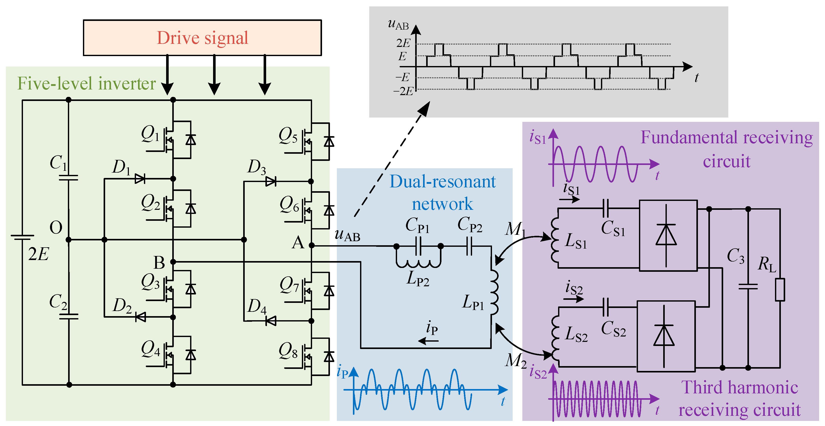
2. WPT System Based on a Multilevel Inverter and Dual-Resonant Network

The proposed system is mainly divided into three parts, as shown in Figure 1.
The first part is the high-frequency inverter link. In this paper, a diode-clamped five-level inverter is used to convert the DC into high-frequency AC where Q1Q8 are MOSFET power switches and D1D4 are clamp diodes. Compared to two-level and three-level inverters, the output voltage of the five-level inverter contains a richer and wider range of controllable harmonics. The second part is a dual-resonant network consisting of capacitor CP1 and inductor LP2 connected in parallel, and then in series, with capacitor CP2 and transmitting coil LP1. The dual-resonant network has two resonant points which can be set to the fundamental and third harmonic frequencies through parameter configuration, allowing for simultaneous power transmission at both frequencies. The third part is the electromagnetic coupling and receiving circuit in the receiving side. There are two receiving channels: the fundamental receiving channel (channel 1) and the third harmonic receiving channel (channel 2). The receiving coil in the fundamental channel is LS1 and the capacitor that resonates with it is CS1. The receiving coil in the third harmonic channel is LS2 and the capacitor that resonates with it is CS2. The mutual inductance of channel 1 is M1 and the mutual inductance of channel 2 is M2. The two receiving channels are connected in parallel after rectification and finally filtered by capacitor C3 to supply power to load resistor RL.

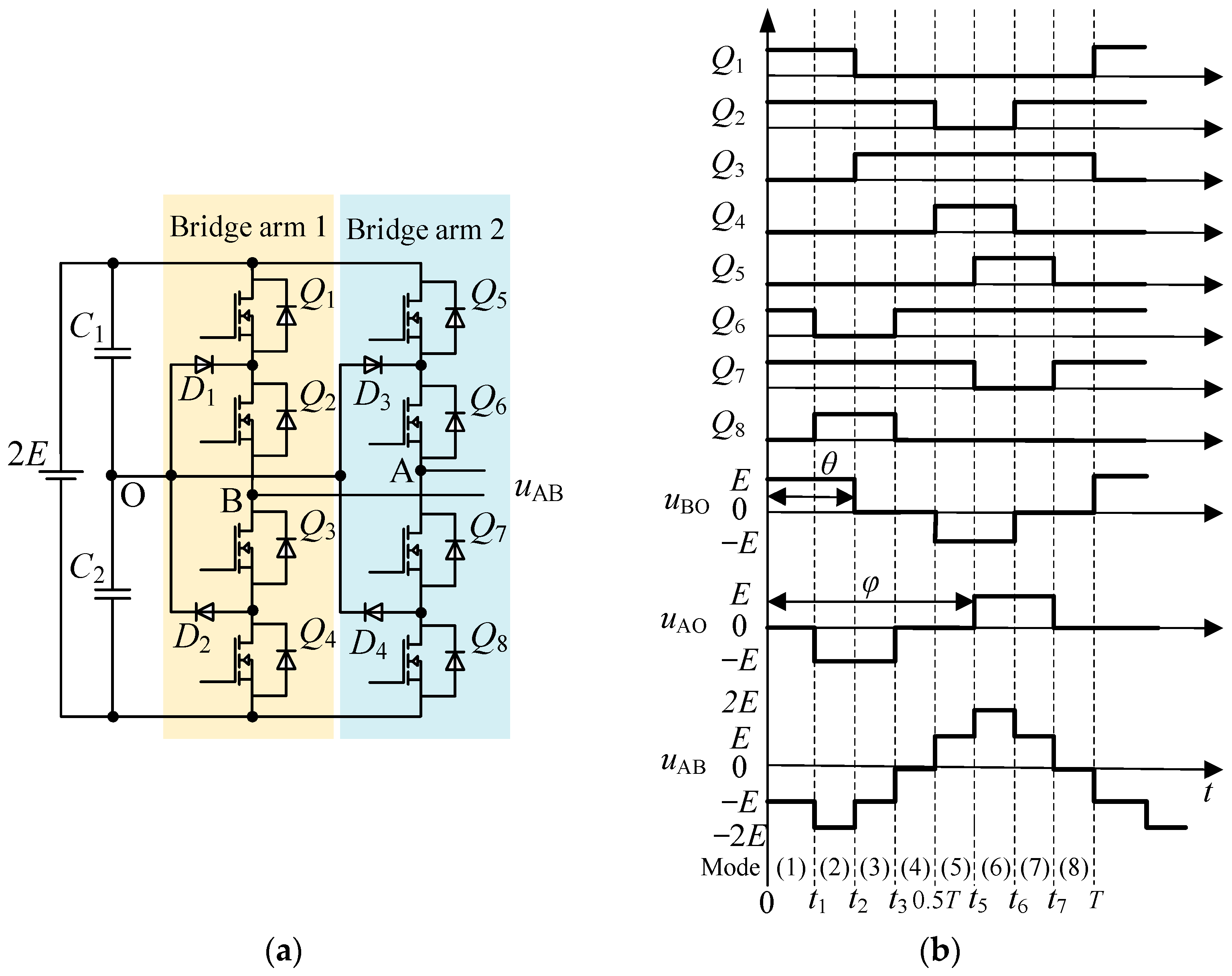
2.1. Five-Level Inverter

The topology of the diode-clamped five-level inverter is shown in Figure 2a, which includes bridge arm 1 and bridge arm 2. Bridge arm 1 generates a three-level voltage uBO through alternating switching of Q1Q4 and bridge arm 2 generates a three-level voltage uAO through alternating switching of Q5Q6. Subtracting the two three-level voltages yields a five-level output voltage uAB. Its main operating waveforms are shown in Figure 2b, where T is the operating cycle. The corresponding operating modes of the five-level inverter are analyzed as follows:
  • Mode 1: Within the time interval of 0-t1, Q1 and Q2 in bridge arm 1 are turned on, Q3 and Q4 are turned off, and point B is connected to the positive end of C1, so uBO = UC1= E. Q5 and Q8 in bridge arm 2 are turned off, Q6 and Q7 are turned on, and point A is connected to point O, so uAO = 0. Therefore, uAB = uAOuBO = −E.
  • Mode 2: Within the time interval of t1-t2, Q1 and Q2 in bridge arm 1 are turned on, Q3 and Q4 are turned off, and point B is connected to the positive end of C1, so uBO = UC1 = E. Q5 and Q6 in bridge arm 2 are turned off, Q7 and Q8 are turned on, and point A is connected to the negative end of C2, so uAO = −E. Therefore, uAB = uAOuBO = −2E.
  • Mode 3: Within the time interval of t2t3, Q2 and Q3 in bridge arm 1 are turned on, Q1 and Q4 are turned off, and point B is connected to point O, so uBO= 0. Q5 and Q6 in bridge arm 2 are turned off, Q7 and Q8 are turned on, and point A is connected to the negative end of C2, so uAO = −E. Therefore, uAB = uAOuBO = −E.
  • Mode 4: Within the time interval of t3-0.5T, Q2 and Q3 in the bridge arm 1 are turned on, Q1 and Q4 are turned off, and point B is connected to point O, so uBO = 0. Q5 and Q8 in the bridge arm 2 are turned off, Q6 and Q7 are turned on, and point A is connected to point O, so uAO = 0. Therefore, uAB = uAOuBO = 0.
  • Mode 5: Within the time interval of 0.5T-t5, Q3 and Q4 in the bridge arm 1 are turned on, Q1 and Q2 are turned off, and point B is connected to the negative end of C2, so uBO = −E. Q5 and Q8 in the bridge arm 2 are turned off, Q6 and Q7 are turned on, and point A is connected to point O, so uAO = 0. Therefore, uAB = uAOuBO = E.
  • Mode 6: Within the time interval of t5t6, Q3 and Q4 in bridge arm 1 are turned on, Q1 and Q2 are turned off, and point B is connected to the negative end of C2, so uBO = E. Q7 and Q8 in bridge arm 2 are turned off, Q5 and Q6 are turned on, and point A is connected to the positive end of C1, so uAO = E. Therefore, uAB = uAOuBO = 2E.
  • Mode 7: Within the time interval of t6t7, Q2 and Q3 in the bridge arm 1 are turned on, Q1 and Q4 are turned off, and point B is connected to point O, so uBO = 0. Q7 and Q8 in the bridge arm 2 are turned off, Q5 and Q6 are turned on, and point A is connected to the positive end of C1, so uAO = E. Therefore, uAB = uAOuBO = E.
  • Mode 8: Within the time interval of t7-T, Q2 and Q3 in the bridge arm 1 are turned on, Q1 and Q4 are turned off, and point B is connected to point O, so uBO = 0. Q5 and Q8 in the bridge arm 2 are turned off, Q6 and Q7 are turned on, and point A is connected to point O, so uAO = 0. Therefore, uAB = uAOuBO = 0.
According to the above analysis, the calculation formula for uAB is
  u AB = u AO u BO
For bridge arm 1 and bridge arm 2, the waveforms of their output voltages uBO and uAO can be expressed by Fourier expansion as
u BO ( t ) = n = 2 k 1 4 E n π sin n θ 2 cos ( n ω t n θ 2 )     u AO ( t ) = n = 2 k 1 4 E n π sin n θ 2 cos ( n ω t n θ 2 n φ ) ( k = 1 , 2 , 3 )
where n is the harmonic order, t is the system operating time, and ω is the operating angular frequency of the inverter. Then, from Equations (1) and (2), the five-level output voltage can be calculated as
u AB ( t ) = n = 2 k 1 8 E n π sin n θ 2 sin ( n φ 2 ) sin ( n ω t + n θ 2 + n φ 2 )
From Equation (3), it can be seen that, when the input DC voltage of the inverter is determined, its output voltage depends on the duty cycle (θ) of the output voltage of the two bridge arms and the phase difference (φ) between the two bridge arms.

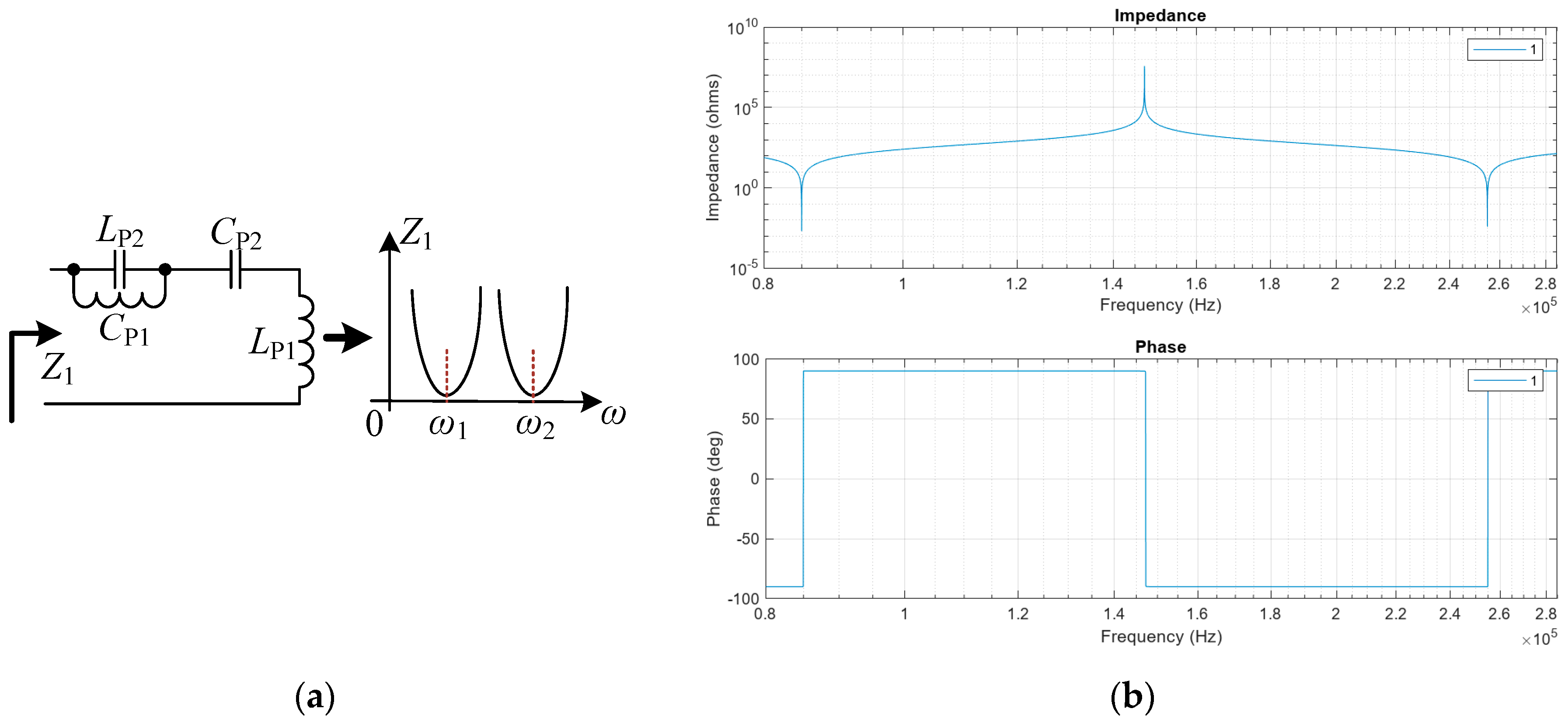
2.2. Dual-Resonant Network

In this paper, a dual-resonant network compensation is used in the transmitting side, as shown in Figure 3a. Its equivalent impedance Z1 can be expressed as
Z 1 = ( j ω L P 2 / / 1 j ω C P 1 ) + 1 j ω C P 2 + j ω L P 1 = j ( ω 4 L P 1 L P 2 C P 1 C P 2 ω 2 ( L P 1 C P 2 + L P 2 C P 1 + L P 2 C P 2 ) + 1 ω 3 L P 2 C P 1 C P 2 ω C P 2 )
According to Equation (4), the impedance characteristics of Z1 can be plotted as shown in Figure 3b. It can be seen that Z1 has two points with minimal impedance values and zero phase, corresponding to two resonant frequencies. When the system is in resonant state, Z1 should be zero, which can be expressed as
ω 4 L P 1 L P 2 C P 1 C P 2 ω 2 L P 1 C P 2 + L P 2 C P 1 + L P 2 C P 2 + 1 = 0
Assuming that the two resonant points of the dual-resonant network are ω1 and ω2, according to the Vieta theorem, the relationship between the two can be calculated as
ω 1 ω 2 = 1 L P 2 C P 1 L P 1 C P 2
Assuming that ω0 is the resonant frequency of LP2 and CP1 as well as the resonant frequency of LP1 and CP2, that is
ω 0 = 1 L P 1 C P 2 1 L P 2 C P 1
By combining Equations (6) and (7), the relationship between ω0, ω1 and ω2 can be obtained as
ω 0 2 = ω 1 ω 2
By substituting Equations (6)–(8) into Equation (5), the relationship between CP1 and CP2 can be obtained as
C P 2 C P 1 = ω 1 2 + ω 2 2 ω 0 2 2
According to the frequency required in this paper, the two resonant frequencies ω1 and ω2 of the dual-resonant network are set to the fundamental and third harmonic frequencies of the inverter output voltage, respectively, in order to achieve the transmission of power at these two frequencies. Therefore, the further relationship between ω0, ω1, and ω2 can be obtained as
ω 2 = 3 ω 1 ω 0 = 3 ω 1
By substituting Equation (10) into (9), the relationship between CP1 and CP2 can be derived as
C P 1 = 3 4 C P 2
The above analysis can solve the problem of fundamental and third harmonic power transfer in the output voltage of the inverter and determine the parameters of the dual-resonant network. When the transmitting coil LP1 is determined, the value of CP2 can be calculated according to Equation (7). Then, the value of CP1 can be determined according to Equation (11). Finally, the value of LP2 can be calculated by Equation (7). Compared with the dual-transmitting and dual-receiving WPT system, the dual-resonant network transmits the fundamental and third harmonics power through the same channel with a simpler structure, which not only improves the output power of the system but also reduces the spatial volume of the system and saves the costs.

3. System Operating Characteristics

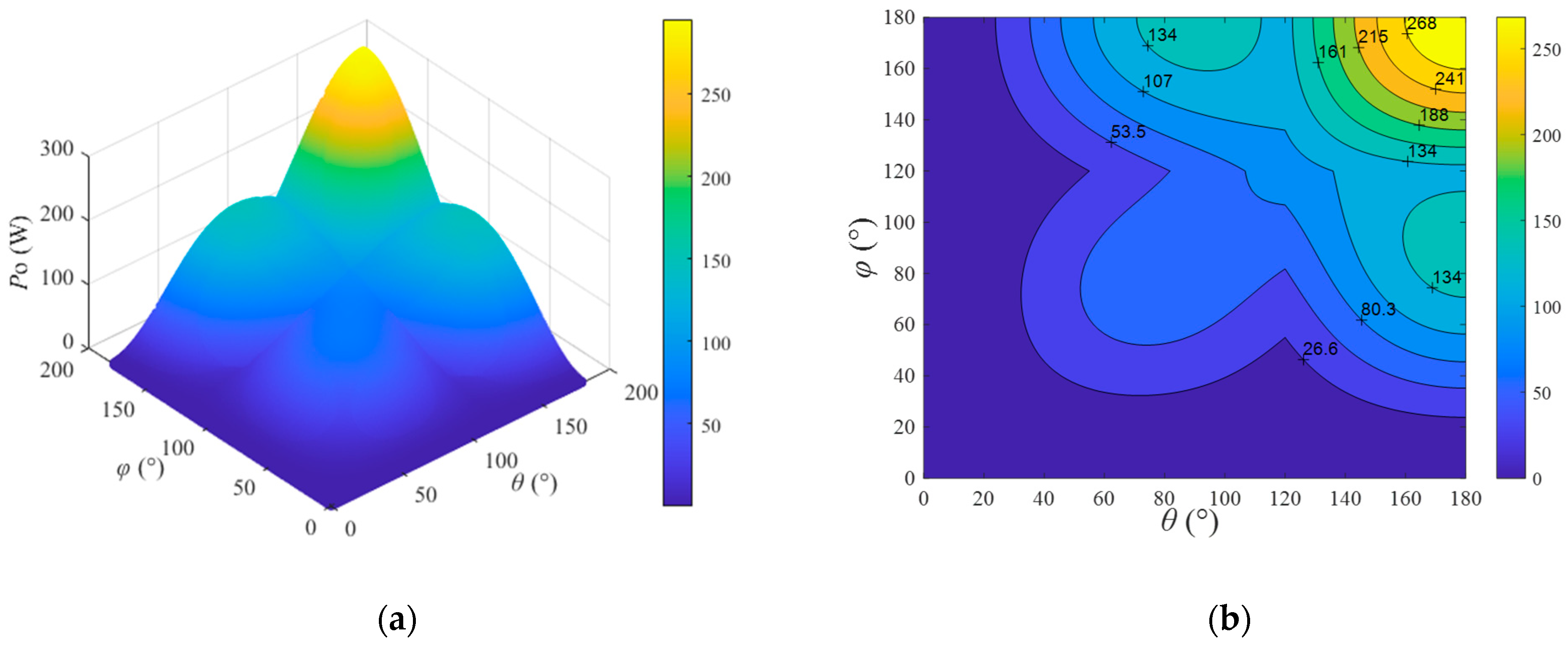
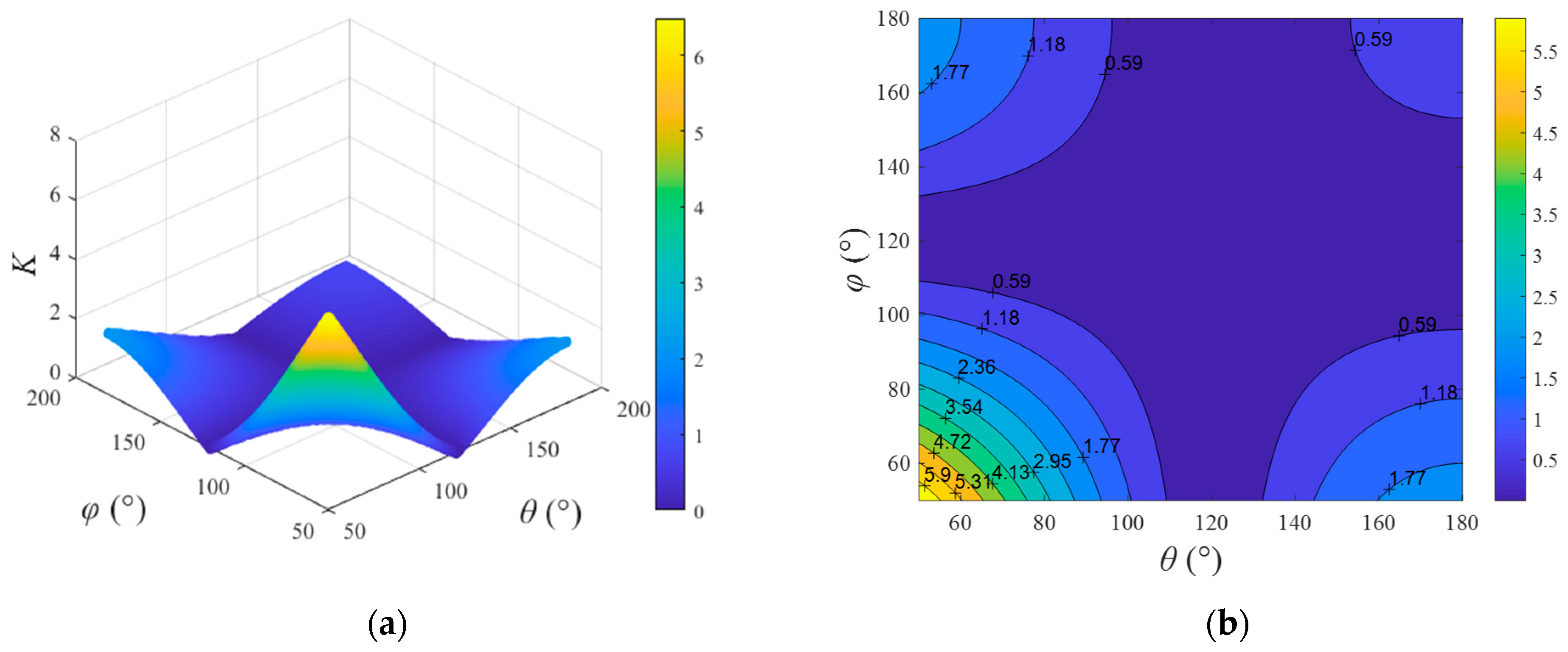
3.1. System Power Boosting Capability

From Equation (3), the RMS value of inverter output voltage can be expressed as
U AB = n = 2 k - 1 4 2 E n π sin n θ 2 sin n φ 2
By substituting k = 1 and k = 3 into Equation (12), the RMS values of the fundamental and third harmonic components of the inverter output voltage can be written as
U AB 1 = 4 2 E π sin θ 2 sin φ 2   U AB 3 = 4 2 E 3 π sin 3 θ 2 sin 3 φ 2
In order to simplify the circuit structure, the load resistor RL is equivalent to the equivalent resistors R1 and R2 in the two receiving circuits before rectification, as shown in Figure 4, where IS1 and IS2 are the RMS values of current in the two receiving coils, US1 and US2 are the RMS values of induced voltage in the two receiving coils, IO1 and IO2 are the currents in the two receiving channels after rectification, and IO is the load current. The two receiving channels of the proposed system are connected in parallel to supply power to the load. Assuming that the output power of the two channels is P1 and P2, respectively, their expressions can be derived from Figure 4 as
P 1 = I O 1 I O 1 + I O 2 I O 2 R L P 2 = I O 2 I O 1 + I O 2 I O 2 R L
By substituting IO = IO1 + IO2 into Equation (14), P1 and P2 can be expressed as
P 1 = I O 1 + I O 2 I O 1 R L P 2 = I O 1 + I O 2 I O 2 R L
Assuming that the rectifier is an ideal component and the power before and after rectification is equal, the relevant equations can be listed as
U S 1 I S 1 = P 1 = I O 1 + I O 2 I O 1 R L U S 2 I S 2 = P 2 = I O 1 + I O 2 I O 2 R L I O 1 = 2 2 π I S 1   ,   I O 2 = 2 2 π I S 2   U S 1 = I S 1 R 1     ,   U S 2 = I S 2 R 2
By simplifying Equation (16), the relationship between the load resistor RL and equivalent resistors R1 and R2 can be derived as
R 1 = 8 I S 1 + I S 2 R L π 2 I S 1 R 2 = 8 I S 1 + I S 2 R L π 2 I S 2    
Due to the significant frequency difference between the fundamental and third harmonics, the two channels can be considered to be decoupled. Therefore, the output power of each channel can be calculated separately first, and then the total output power can be obtained by adding the two. The equivalent circuits of the fundamental and third harmonic channels are shown in Figure 5, where IP1 and IP2 are the RMS values of the transmitting coil currents in the two channels, respectively.
The reflected impedance mapped from the receiving side to the transmitting side in the fundamental channel equivalent circuit is denoted as ZO1, which can be expressed as
Z O 1 = ω 1 2 M 1 2 R 1
Based on this, the expressions for IP1, US1, and IS1 can be obtained as
I P 1 = U AB 1 Z O 1 = U AB 1 R 1 ω 1 2 M 1 2 U S 1 = ω 1 M 1 I P 1 = U AB 1 R 1 ω 1 M 1 I S 1 = U S 1 R 1 = U AB 1 ω 1 M 1  
From US1 and IS1, the output power of the fundamental channel can be calculated as
P 1 = I S 1 U S 1 = U AB 1 2 R 1 ω 1 2 M 1 2
Similarly, the output power of the third harmonic channel can be calculated as
P 2 = I S 2 U S 2 = U AB 3 2 R 2 9 ω 1 2 M 2 2  
Finally, the total output power of the system is
P O = P 1 + P 2 = 8 R L π 2 3 M 2 U AB 1 + M 1 U AB 3 3 ω 1 M 1 M 2 2
According to Equation (22), when RL, M1, M2, and ω1 are determined, PO is only related to the output voltage of the inverter, so PO can be freely adjusted by changing θ and φ. A three-dimensional graph and contour map of PO varying with θ and φ can be drawn as shown in Figure 6, where the DC input voltage is 180 V, the mutual inductance M1 is 67 μH, M2 is 22.4 μH, ω1 is 170,000π rad/s, and RL is 10 Ω. From the figure, it can be seen that, as θ and φ increase simultaneously, PO also increases and multiple different combinations of θ and φ can produce the same PO, indicating that the controllability and degree of freedom of the system output power are very high.
For the conventional WPT system, which has only one fundamental channel in the receiving side, the output power POC can be expressed as
P OC = 8 U AB 1 2 R L π 2 ω 1 2 M 1 2
To describe the power boosting capability of the proposed method, the parameter K is introduced as the power boosting coefficient, which can be expressed as
K = P O P OC P OC = 3 M 2 U AB 1 + M 1 U AB 3 3 ω 1 M 1 M 2 2 U AB 1 2 ω 1 2 M 1 2 U AB 1 2 ω 1 2 M 1 2 = 6 M 1 M 2 U AB 1 U AB 3 + M 1 2 U AB 3 2 9 M 2 2 U AB 1 2
According to Equation (24), the three-dimensional graph and contour map of K varying with θ and φ can be plotted as shown in Figure 7. It can be seen that, compared to the single-channel system, the proposed method can effectively improve the system output power throughout the entire output power range. In the low-output-power range, the proposed method can increase the power by more than five times, and in the high-output-power range, the improvement can exceed 50%.

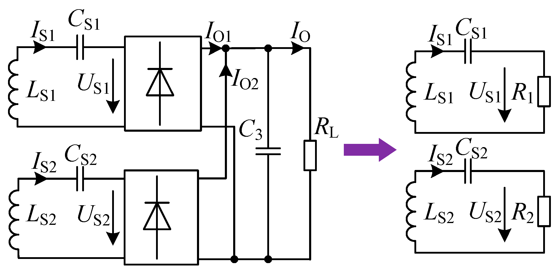
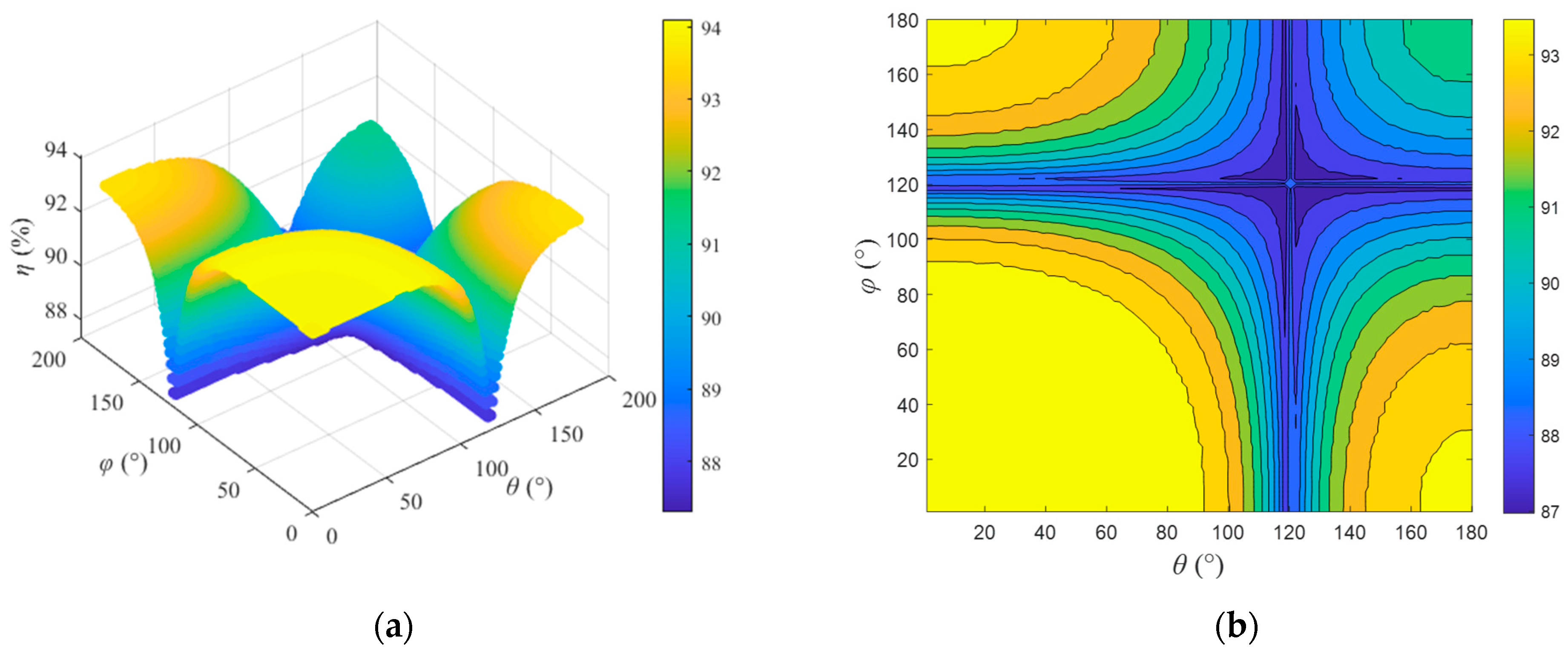
3.2. System Efficiency

From Figure 6, it can be seen that the system will produce contours of PO in the plane constituted by θ and φ. Therefore, one of the problems that this paper needs to solve is how to select the appropriate θ and φ to achieve higher system efficiency at the same PO.
Assuming that the internal resistor of LP1 is RP and that the internal resistors of LS1 and LS2 are RS1 and RS2, respectively, the power loss of the coupling mechanism is
P LOSS = I P 2 R P + I S 1 2 R S 1 + I S 2 2 R S 2
where IP is the RMS value of the transmitting coil current, and its instantaneous value iP is composed of the instantaneous values of the fundamental current iP1 and the third harmonic current iP2. Therefore, the calculation formula for IP is
I P = R M S i P 1 + i P 2
where the expressions of iP1 and iP2 can be written as
i P 1 = u AB 1 ( t ) Z O 1 = u AB 1 ( t ) R 1 ω 1 2 M 1 2 = 8 E R 1 π ω 1 2 M 1 2 sin θ 2 sin φ 2 sin ( - ω t + θ 2 + φ 2 ) i P 2 = u AB 3 ( t ) Z O 2 = u AB 3 ( t ) R 2 9 ω 1 2 M 2 2 = 8 E R 2 9 π ω 1 2 M 2 2 sin 3 θ 2 sin 3 φ 2 sin ( - 3 ω t + 3 θ 2 + 3 φ 2 )
Then, PLOSS can be further rewritten as
P LOSS = R M S i P 1 + i P 2 2 R P + U AB 1 2 ω 1 2 M 1 2 R S 1 + U AB 3 2 9 ω 1 2 M 2 2 R S 2
Finally, the system efficiency η is
η = P O P O + P LOSS × 100 %
According to Equation (29), the three-dimensional graph and contour map of η varying with θ and φ can be obtained as shown in Figure 8. Based on the analysis of Figure 6 and Figure 8, it can be seen that, under the same output power, the system efficiency will vary with different θ and φ. Therefore, it is necessary to select appropriate operating points of the inverter to ensure that the system operates in an optimized state.

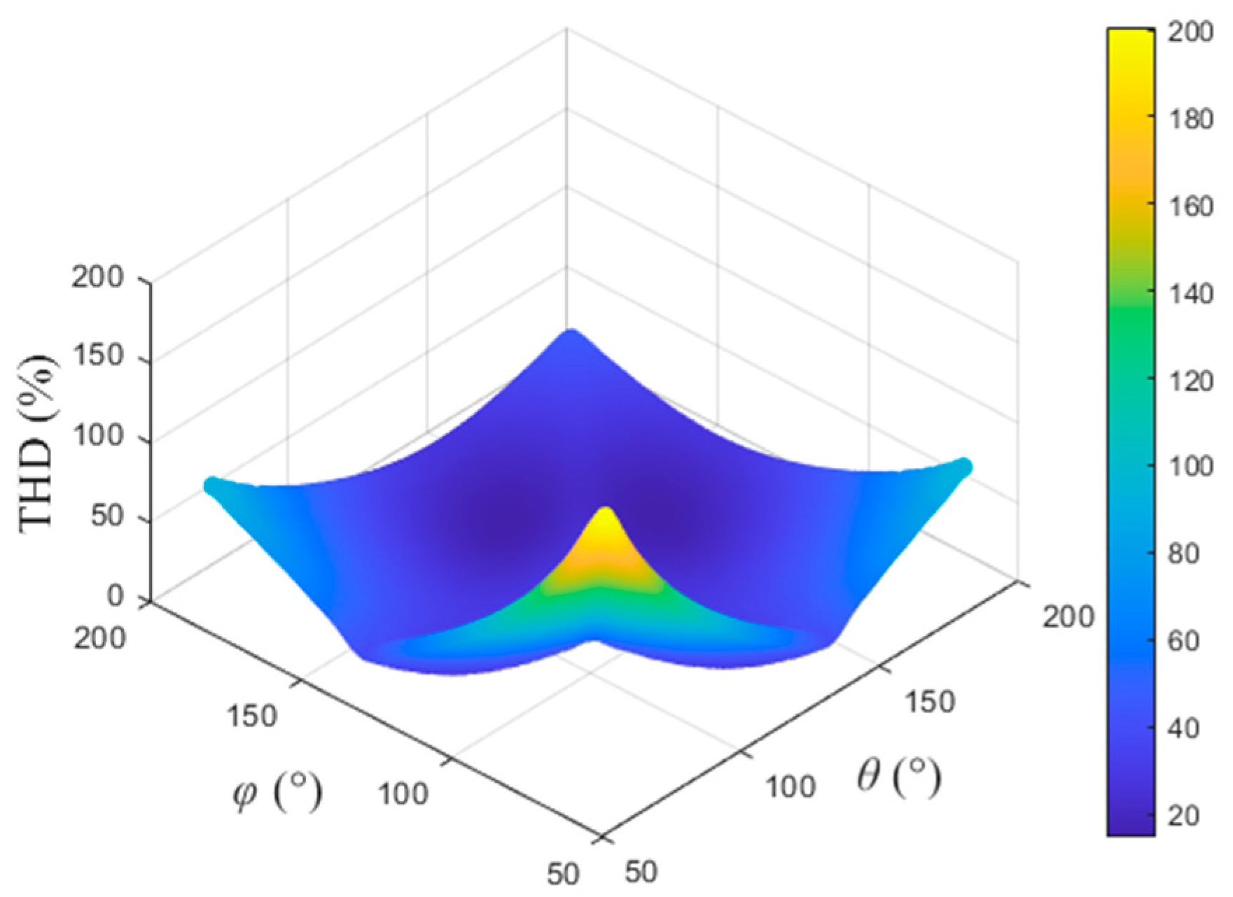
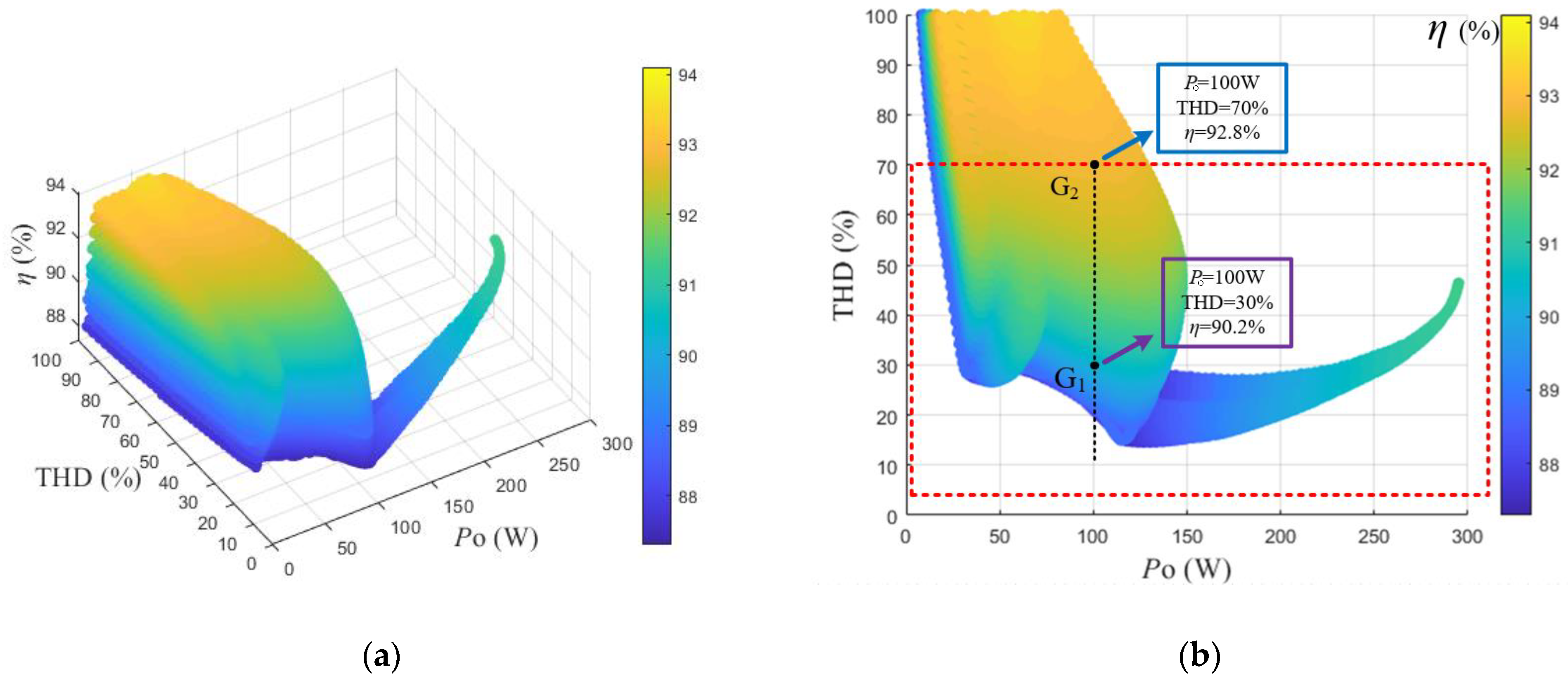
3.3. Selection of Inverter Operating Points

The proposed method improves the system output power by utilizing harmonics. Therefore, to achieve better performance in the system, when selecting the operating points of the inverter, both the system efficiency and the THD of the inverter output voltage should be considered, as high efficiency and low THD are basic requirements for engineering applications. Based on Equation (12), the expression for the THD of the inverter output voltage can be written as
THD = n = 3 , 5 , 7 , U AB n 2 U AB 1
According to Equation (30), a three-dimensional graph of the inverter output voltage THD as a function of θ and φ can be drawn as shown in Figure 9. It can be seen that, the larger the θ and φ, the lower the THD; otherwise, the THD will be higher. When the THD is high, the output voltage of the inverter not only contains rich third harmonic, but also increases the content of fifth, seventh, and higher harmonics.
Based on the above analysis, a three-dimensional graph of the relationship between system output power, system efficiency, and inverter output voltage THD can be further drawn as shown in Figure 10a. It can be seen that, within the entire output power range, the higher the efficiency, the higher the THD, indicating that the two are contradictory. At low power levels, the THD is high and may interfere with the safe operation of the system. In order to improve the power transmission quality and ensure the safe operation of the inverter and other power electronic devices, the selection rules for the optimal operating points of the inverter are as follows: When the output power is low, the point that the THD is not exceeding 70% and the efficiency is highest is selected as the operating point of the inverter. When the output power is high, it can be seen that the maximum THD value is below 70%. At this time, the point with the highest efficiency is directly selected as the operating point of the inverter, which is the part in the red box in Figure 10b. Taking an output power of 100 W as an example, as shown in points G1 and G2 in the figure, the output power is the same and the THD is within 70%. The system efficiency at point G1 is 90.2% and the THD is 30%, while the system efficiency at G2 is 92.8% and the THD is 70%. Therefore, G2 is selected as the optimal operating point of the inverter at an output power of 100 W.

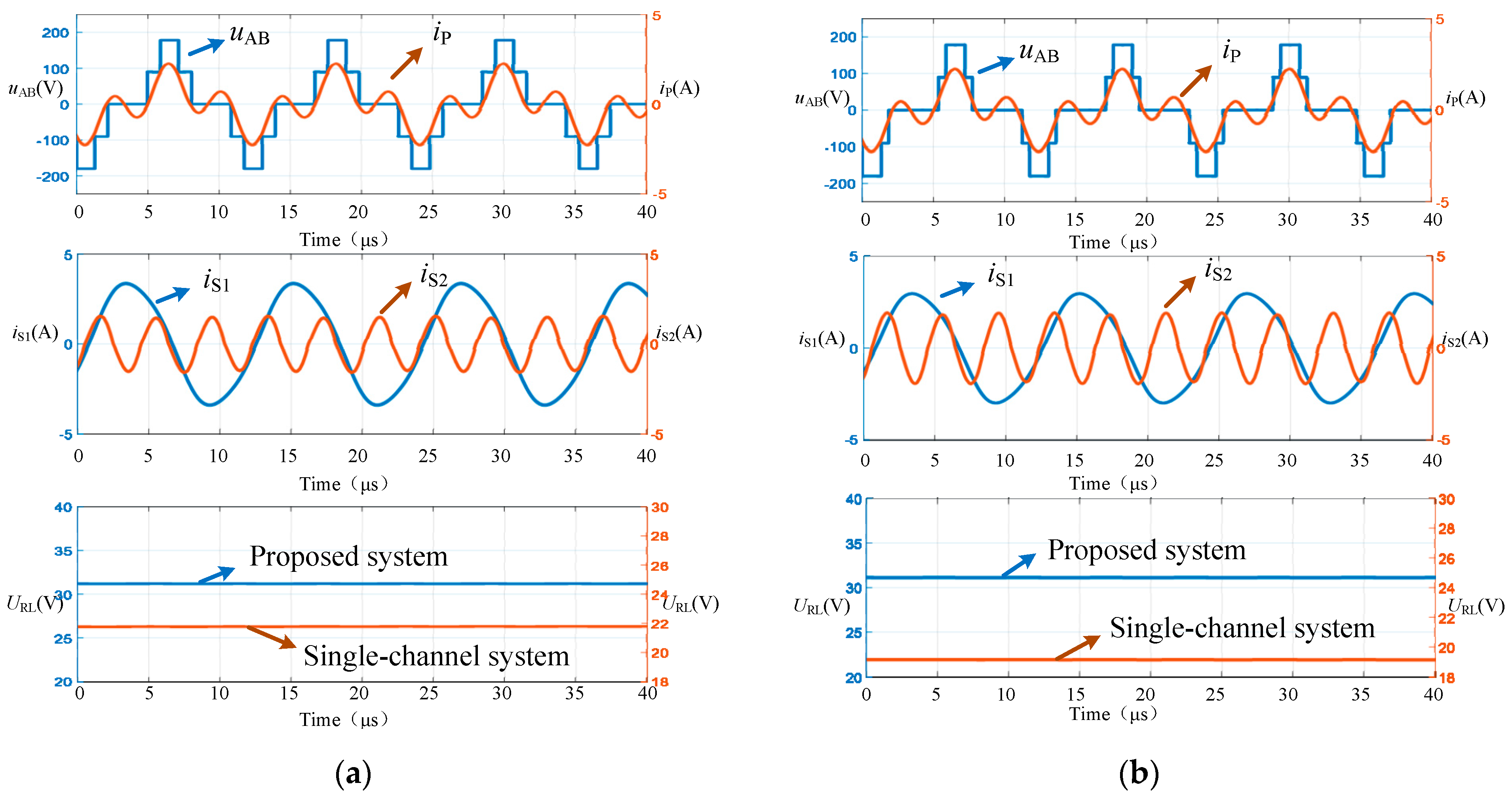
4. Simulation Verification

Based on the system parameters in Table 1, the proposed method is simulated and verified using the Matlab/Simulink 2023b simulation platform.
According to the analysis results in the previous section, at operating point G1, θ and φ are set to 67 ° and 152 °, respectively. At operating point G2, θ and φ are set to 57 ° and 164 °, respectively. The simulation waveforms are shown in Figure 11, where (a) is the simulation waveforms at operating point G1 and (b) is the simulation waveforms at operating point G2. It can be seen that the inverter can generate different five-level output voltages under different modulation parameters. The output current of the inverter is mainly composed of fundamental and third harmonic components. The receiving currents of the fundamental and third harmonic receiving channels are both sine waves and their frequencies differ by three times. Under different modulation parameters, the fundamental and third harmonic contents of the inverter output voltage are also different, so the magnitude of the receiving current values in the fundamental and third harmonic receiving channels also varies. The figure also shows the load voltage of the proposed system and the load voltage of the traditional single-channel WPT system. It can be seen that the system output power is improved to a certain extent under two different operating points. The higher the third harmonic content, the more pronounced the power improvement, but it can also affect the THD of the inverter output voltage. The THD of the inverter output voltage at two operating points is shown in Figure 12, which is consistent with the theoretical analysis.
The related operating parameters of the system are shown in Table 2. The input DC voltage is 180 V, the output voltage THD of the inverter at operating point G1 is 32.18%, and the output voltage THD of the inverter at operating point G2 is 70.87%. At the operating point G1, the proposed system increases the output power from 67.6 W of the single-channel system to 97.9 W with a boost coefficient of approximately 0.45. At the operating point G2, the system output power is increased from 49.7 W of the single-channel system to 97.3 W with a boost coefficient of approximately 0.96. The power enhancement capability of operating point G2 is stronger than that of operating point G1. Although operating point G1 has a lower THD, operating point G2 has stronger power enhancement capability and higher system efficiency. Within the allowable range of THD, operating point G2 conforms to the optimal operating point analyzed earlier, which verifies the effectiveness of theoretical analysis.

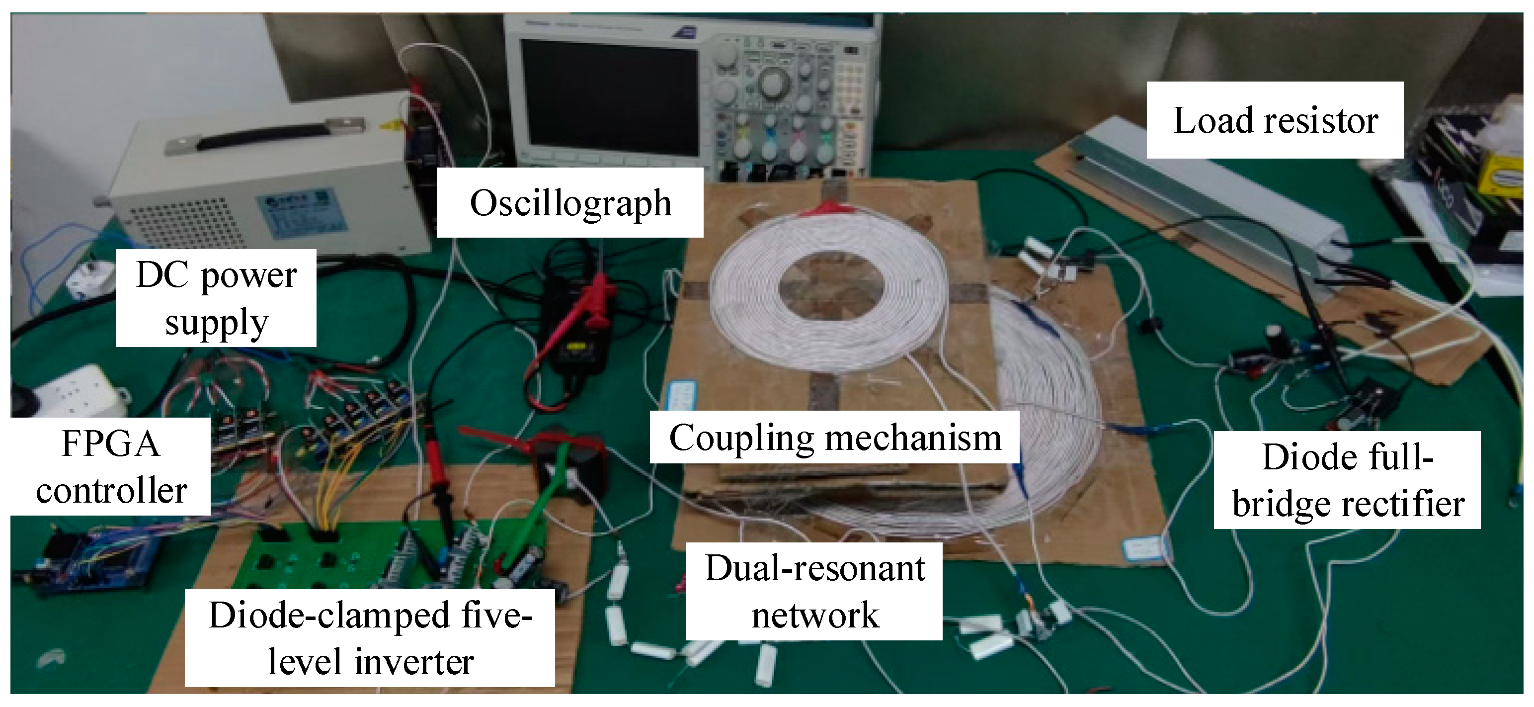
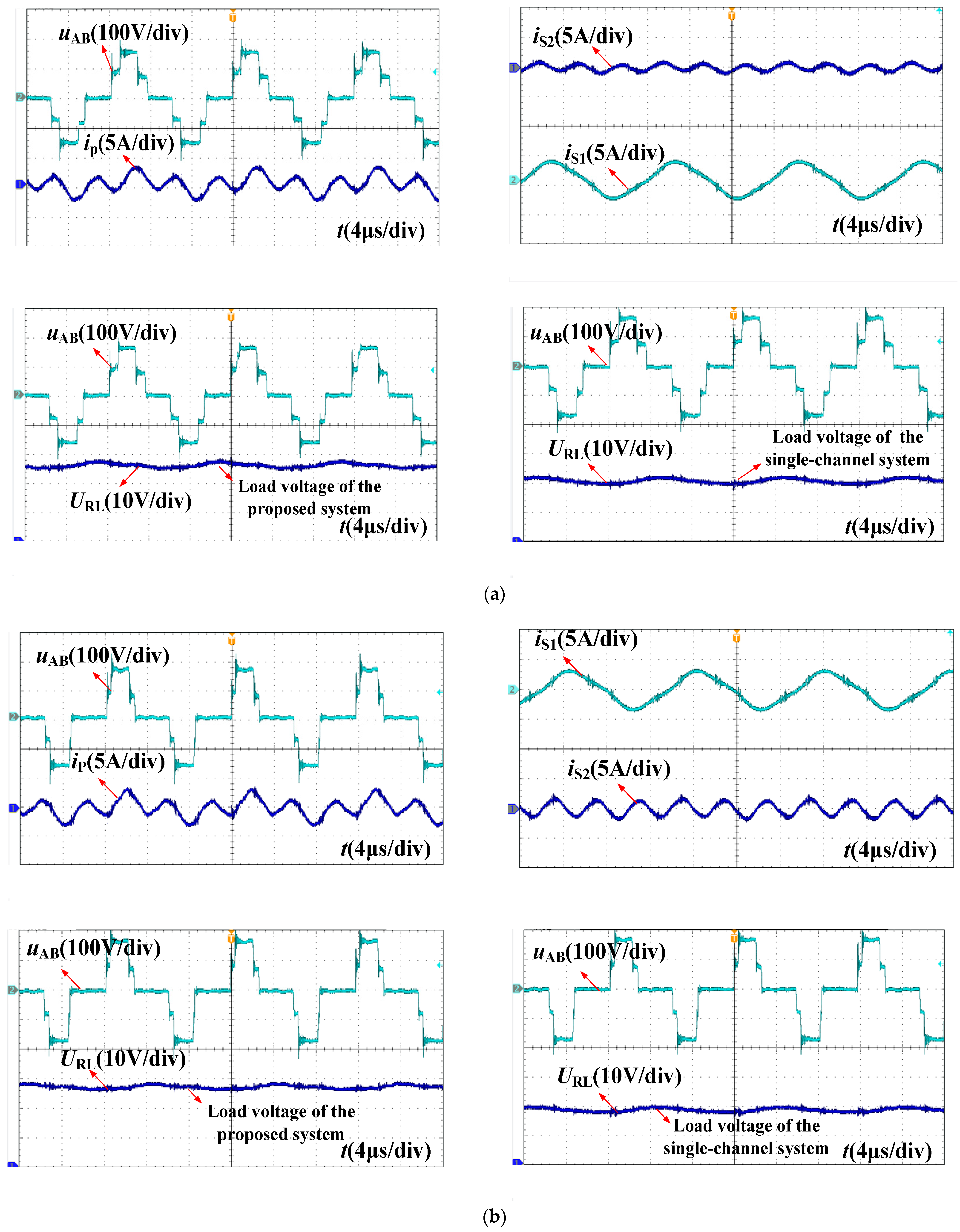
5. Experimental Verification

In order to verify the superiority and effectiveness of the proposed method for boosting the system output power, an experimental setup, as shown in Figure 13, is constructed based on the system parameters in Table 1. The experimental setup mainly consists of a DC power supply, an FPGA controller, a diode-clamped five-level inverter, a dual-resonant network, a coupling mechanism, two diode full-bridge rectifiers, and a load resistor. The FPGA controller is used to generate driving signals to control Q1Q8 MOSFET power switches. The coupling mechanism has two receiving coils on either side of the transmitting coil to reduce cross coupling between the two.
The experimental waveforms are shown in Figure 14, where Figure 14a is the experimental waveforms at operating point G1. The inverter output voltage is a five-level waveform with a maximum amplitude of 180 V. The inverter output current is composed of fundamental and third harmonic components. iS1 and iS2 are the receiving currents of the fundamental and third harmonic channels, respectively. Due to the low third harmonic component in the inverter output voltage, iS1 is significantly higher than iS2. The experimental results are consistent with the simulation. At the same time, the load voltage waveforms of the proposed system and the traditional single-channel WPT system are measured separately. Under the same input DC voltage, the output power of the proposed system is significantly improved compared to the traditional single-channel WPT system. Similarly, Figure 14b shows the experimental waveforms at the operating point G2, which are consistent with the simulation results. The system output power has been significantly improved, and the improvement effect is consistent with the theoretical analysis and simulation results.
Table 3 compares the proposed method with existing power boosting methods, including inverters, resonant compensation networks, the number of coils, the operating principle, the output power, maximum efficiency, power boosting coefficients, and system complexity. It can be seen from the table that the literature [11,12,13] seeks the maximum power point through impedance matching. However, the power level is low, and increasing the power may lead to decreased efficiency. The literature [20,21] utilizes high-capacity inverters to increase the transmitting current. However, parallel inverters may affect the system’s performance due to circulating currents, and three-phase inverters may cause significant harmonic currents due to phase imbalance. The literature [27,28] improves the system output power by constructing multiple transmission channels with higher power levels; however, this requires more resonant compensation networks and coils, resulting in a larger system volume and higher system complexity. The proposed method in this paper adopts a dual-resonant network which can simultaneously transmit the power of two frequencies generated by a multilevel inverter with only one transmitting coil, requiring fewer components. Therefore, the complexity is lower compared to other examples from the literature. Moreover, the proposed method has significant advantages regarding the power boosting coefficient and can maintain high efficiency.

6. Summary

This paper proposes a power boosting method for WPT systems based on a multilevel inverter and dual-resonant network. The high-frequency inverter adopts a five-level inverter which can generate more abundant and controllable harmonics over a wide range compared to the full-bridge inverter. The transmitting compensation network adopts a dual-resonant network which can complete the transmission of dual-frequency power with fewer components and smaller volumes compared to the existing dual-frequency power synthesis and transmission methods, thereby effectively improving the system output power. This paper first introduces the topology and operating principle of the proposed system. Then, the relationship between the output voltage and modulation parameters of the five-level inverter is explained by analyzing its operating modes. Next, the parameter design method of the dual-resonant network is obtained through analysis and calculation and the performance curve of the system output power improvement is obtained by analyzing the operating characteristics of the system. Subsequently, based on the requirements of the inverter output voltage THD and system efficiency, the optimal operating point selection strategy for the inverter is designed under the same output power. Finally, simulation and experimental verification are conducted and compared with the traditional single-channel WPT system. The results show that the proposed system can boost the output power from 160 W to 310 W, almost doubling the amount, verifying the superiority and feasibility of the proposed method.

Author Contributions

Conceptualization, X.G.; methodology, X.G.; software, Y.W.; validation, Y.W. and M.T.; formal analysis, Y.W.; investigation, X.G. and Y.W.; resources, X.G.; data curation, Y.W. and M.T.; writing—original draft preparation, Y.W.; writing—review and editing, X.G.; visualization, Y.W.; supervision, X.G. and L.W.; project administration, X.G. and L.W.; funding acquisition, X.G. All authors have read and agreed to the published version of the manuscript.

Funding

This research was funded by the Jiangsu Provincial University (Natural Science) Foundation and Talent Startup Funding of Wuxi University, grant number 24KJB470027 and 2021r044, respectively.

Data Availability Statement

Data are contained within the article.

Conflicts of Interest

The authors declare no conflicts of interest.

References

  1. Feng, H.; Tavakoli, R.; Onar, O.C.; Pantic, Z. Advances in High-Power Wireless Charging Systems: Overview and Design Considerations. IEEE Trans. Transp. Electrif. 2020, 6, 886–919. [Google Scholar] [CrossRef]
  2. Zhang, Y.; Pan, W.; Wang, H.; Shen, Z.; Wu, Y.; Dong, J.; Mao, X. Misalignment-Tolerant Dual-Transmitter Electric Vehicle Wireless Charging System with Reconfigurable Topologies. IEEE Trans. Power Electron. 2022, 37, 8816–8819. [Google Scholar] [CrossRef]
  3. Liu, Y.; Li, Y.; Zhang, X.; He, Z. Load-Independent Voltage-Gain Design Method for Domino-Resonator Wireless Power Transfer Systems. IEEE Trans. Power Electron. 2024, 39, 1997–2003. [Google Scholar] [CrossRef]
  4. Xia, C.; Zhang, H.; Wei, N.; Zhao, S.; Yan, J.; Song, X.; Xiang, L.; Liao, Z. Simultaneous Wireless Power and Multibit Signals Transfer System with Hybrid Modulation Waves PWM Control. IEEE Trans. Power Electron. 2022, 37, 12913–12928. [Google Scholar] [CrossRef]
  5. Zhou, Y.; Zhang, Z.; Dong, P.; Chen, Y.; Huang, L. Simultaneous Wireless Power and Data Transmission Based on Unsymmetrical Current Waveforms with Duty Cycle Modulation. IEEE Access 2020, 8, 16495–16504. [Google Scholar] [CrossRef]
  6. Cairo, J.I.; Bonache, J.; Paredes, F.; Martin, F. Reconfigurable System for Wireless Power Transfer (WPT) and Near Field Communications (NFC). IEEE J. Radio Freq. Identif. 2017, 1, 253–259. [Google Scholar] [CrossRef]
  7. Jiang, J.; Li, Z.; Song, K.; Song, B.; Dong, S.; Zhu, C. A Cascaded Topology and Control Method for Two-Phase Receivers of Dynamic Wireless Power Transfer Systems. IEEE Access 2020, 8, 47445–47455. [Google Scholar] [CrossRef]
  8. Kung, M.-L.; Lin, K.-H. A Dual-Band Wireless Power Transfer System with Efficiency-Boosting Converter. IEEE Microw. Wireless Compon. Lett. 2020, 30, 1108–1111. [Google Scholar] [CrossRef]
  9. Le-Huu, H.; Seo, C. A Hybrid Transmitting Coil for Improving Angular Freedom of a Wireless Power Transfer System. IEEE Microw. Wireless Technol. Lett. 2024, 34, 119–122. [Google Scholar] [CrossRef]
  10. Dan, Z.; He, Z.; Lin, H.; Liu, C. A Patch Rectenna with an Integrated Impedance Matching Network and a Harmonic Recycling Filter. Antennas Wirel. Propag. Lett. 2022, 21, 2085–2089. [Google Scholar] [CrossRef]
  11. Dai, X.; Li, X.; Hu, A.P. Impedance-Matching Range Extension Method for Maximum Power Transfer Tracking in IPT System. IEEE Trans. Power Electron. 2018, 33, 4419–4428. [Google Scholar] [CrossRef]
  12. Chung, E.; Ha, J.-I. Impedance Matching Network Design for 6.78-MHz Wireless Power Transfer System with Constant Power Characteristics Against Misalignment. IEEE Trans. Power Electron. 2024, 39, 1788–1801. [Google Scholar] [CrossRef]
  13. Esfahani, F.N.; Madani, S.M.; Niroomand, M.; Safaee, A. Maximum Wireless Power Transmission Using Real-Time Single Iteration Adaptive Impedance Matching. IEEE Trans. Circuits Syst. I 2023, 70, 3806–3817. [Google Scholar] [CrossRef]
  14. Wu, J.; Dai, X.; Sun, Y.; Li, Y. A Node Role Dynamic Change Method Among Repeater, Receiver, and Decoupling Using Topology Switching in Multinode WPT System. IEEE Trans. Power Electron. 2021, 36, 11174–11182. [Google Scholar] [CrossRef]
  15. Wu, J.; Dai, X.; Gao, R.; Jiang, J. A Coupling Mechanism with Multidegree Freedom for Bidirectional Multistage WPT System. IEEE Trans. Power Electron. 2021, 36, 1376–1387. [Google Scholar] [CrossRef]
  16. Wang, L.; Li, J.; Chen, H.; Pan, Z. Radial-Flux Rotational Wireless Power Transfer System with Rotor State Identification. IEEE Trans. Power Electron. 2022, 37, 6206–6216. [Google Scholar] [CrossRef]
  17. Shu, X.; Zhang, B.; Wei, Z.; Rong, C.; Sun, S. Extended-Distance Wireless Power Transfer System with Constant Output Power and Transfer Efficiency Based on Parity-Time-Symmetric Principle. IEEE Trans. Power Electron. 2021, 36, 8861–8871. [Google Scholar] [CrossRef]
  18. Gao, X.; Liu, C.; Zhou, H.; Hu, W.; Huang, Y.; Xiao, Y.; Lei, Z.; Chen, J. Design and Analysis of a New Hybrid Wireless Power Transfer System with a Space-Saving Coupler Structure. IEEE Trans. Power Electron. 2021, 36, 5069–5081. [Google Scholar] [CrossRef]
  19. Guo, Z.; Yang, F.; Zhang, H.; Wu, X.; Wu, Q.; Zhu, K.; Jiang, J.; Jiang, H.; Yang, Y.; Li, Y.; et al. Level Pinning of Anti-PT-Symmetric Circuits for Efficient Wireless Power Transfer. Natl. Sci. Rev. 2024, 11, 215–224. [Google Scholar] [CrossRef]
  20. Liu, H.; Wang, Y.; Yu, H.; Wu, F.; Wheeler, P. A Novel Three-Phase Omnidirectional Wireless Power Transfer System with Zero-Switching-Loss Inverter and Cylindrical Transmitter Coil. IEEE Trans. Power Electron. 2023, 38, 10426–10441. [Google Scholar] [CrossRef]
  21. Chowdhury, S.; Tarek, M.T.B.; Haque, M.E.; Sozer, Y. A Three-Phase Overlapping Winding–Based Wireless Charging System for Transportation Applications. IEEE Trans. Power Electron. 2023, 38, 16245–16255. [Google Scholar] [CrossRef]
  22. Song, C.; Kim, H.; Kim, Y.; Kim, D.; Jeong, S.; Cho, Y.; Lee, S.; Ahn, S.; Kim, J. EMI Reduction Methods in Wireless Power Transfer System for Drone Electrical Charger Using Tightly Coupled Three-Phase Resonant Magnetic Field. IEEE Trans. Ind. Electron. 2018, 65, 6839–6849. [Google Scholar] [CrossRef]
  23. Mehta, P.; Sahoo, S.; Bharadwaj, P. Fault Tolerant High-Frequency Multilevel Inverter for Wireless EV Charging. In Proceedings of the 2023 IEEE 3rd International Conference on Smart Technologies for Power, Energy and Control (STPEC), Bhubaneswar, India, 10–13 December 2023; IEEE: Piscataway, NJ, USA, 2023; pp. 1–6. [Google Scholar]
  24. Lee, E.-J.; Lee, K.-B. Modulation Methods based on Phase-Shifted PWM for H- Bridge Multilevel Inverters. In Proceedings of the 2020 IEEE PELS Workshop on Emerging Technologies: Wireless Power Transfer (WoW), Seoul, Republic of Korea, 15–19 November 2020; IEEE: Piscataway, NJ, USA, 2020; pp. 189–193. [Google Scholar]
  25. Zhang, Z.; Li, X.; Pang, H.; Komurcugil, H.; Liang, Z.; Kennel, R. Multiple-Frequency Resonating Compensation for Multichannel Transmission of Wireless Power Transfer. IEEE Trans. Power Electron. 2021, 36, 5169–5180. [Google Scholar] [CrossRef]
  26. Li, X.; Zhang, Z.; Si, W.; Wang, R.; Liang, Z. Analysis and Optimization of Equivalent Load for Multichannel Transmission of Wireless Power Transfer. IEEE Trans. Magn. 2021, 57, 1–6. [Google Scholar] [CrossRef]
  27. Ibrahim, A.U.; Zhong, W.; Xu, M.D. A 50-kW Three-Channel Wireless Power Transfer System with Low Stray Magnetic Field. IEEE Trans. Power Electron. 2021, 36, 9941–9954. [Google Scholar] [CrossRef]
  28. Liang, Y.; Sun, P.; Yang, G.; Sun, J.; Cai, J.; Wu, X.; Deng, Q. Analysis and Parameter Design for Input-Series Output-Series (ISOS) Multichannel Inductive Power Transfer System Considering Cross Coupling. IEEE J. Emerg. Sel. Top. Power Electron. 2024, 12, 2361–2376. [Google Scholar] [CrossRef]
Figure 1. Structural diagram of the proposed WPT system.
Electronics 13 04066 g001
Figure 2. Diode-clamped five-level inverter. (a) Topology; (b) main operating waveforms.
Electronics 13 04066 g002
Figure 3. Dual-resonant network. (a) Topology; (b) impedance characteristics.
Electronics 13 04066 g003
Figure 4. Equivalent circuit of the receiving side.
Electronics 13 04066 g004
Figure 5. Equivalent circuits of fundamental and third harmonic channels. (a) Fundamental; (b) third harmonic.
Electronics 13 04066 g005
Figure 6. Variation in PO with θ and φ. (a)Three-dimensional graph; (b) contour map.
Electronics 13 04066 g006
Figure 7. Variation in K with θ and φ. (a) Three-dimensional graph; (b) contour map.
Electronics 13 04066 g007
Figure 8. Variation in η with θ and φ. (a) Three-dimensional diagram; (b) contour diagram.
Electronics 13 04066 g008
Figure 9. Variation in the THD of the inverter output voltage with θ and φ.
Electronics 13 04066 g009
Figure 10. (a) Three-dimensional graph of the PO, THD and η; (b) selection of the optimal operating point.
Electronics 13 04066 g010
Figure 11. Simulation waveforms. (a) Operating point G1; (b) operating point G2.
Electronics 13 04066 g011
Figure 12. THD of inverter output voltage. (a) Operating point G1; (b) operating point G2.
Electronics 13 04066 g012
Figure 13. Experimental setup.
Electronics 13 04066 g013
Figure 14. Experimental waveforms. (a) At operating point G1; (b) at operating point G2.
Electronics 13 04066 g014
Table 1. System parameters.
ParametersValueParametersValue
Uin/V180CS1/nF7
CP1/nF2.85LS2/μH55.64
CP2/nF3.8CS2/nF7
LP1/μH307.6M1/μH67
LP2/μH410.2M2/μH22.4
C1/μF220RP0.35
C2/μF220RS10.6
C3/μF100RS20.25
LS1/μH500.85RL10
Table 2. Operating parameters of the system under two operating points G1 and G2.
Operating PointsInput DC Voltage (V)THD of Inverter Output VoltageProposed System Output Power (W)Single-Channel System Output Power (W)EfficiencyPower Boosting Coefficient
G118032.18%97.967.689.5%0.45
G218070.87%97.349.792.2%0.96
Table 3. Comparison with existing power boosting methods.
RefInverterResonant Compensation NetworkNumber of CoilsOperating PrincipleOutput PowerMaximum EfficiencyPower Boosting CoefficientSystem Complexity
[11]Full-bridgeS-S2Impedance matching30–40 W44.7%L 1L
[12]Single-ended switch inverterS-S230–45 W95%LL
[13]-S-S220 W90%LM
[14]Full-bridgeLCC-LCC3Topology switching175.7 W94.2%ML
[20]Parallel of full-bridgeLCC-S4Increasing transmitting current93.4–104.7 W78.1%M 2H
[21]Three-phase inverterS-S67.7 KW94.9%H 3H
[27]-S-S6Multiple channels50 KW95.2%HH
[28]Full-bridgeS-S62.81 KW92.44%HH
This workMultilevel inverterDual-resonant network3Harmonic utilization + Multiple channels310 W92.2%HM
1 Low. 2 Medium. 3 High.
Disclaimer/Publisher’s Note: The statements, opinions and data contained in all publications are solely those of the individual author(s) and contributor(s) and not of MDPI and/or the editor(s). MDPI and/or the editor(s) disclaim responsibility for any injury to people or property resulting from any ideas, methods, instructions or products referred to in the content.

