High-Speed Signal Optimization at Differential VIAs in Multilayer Printed Circuit Boards
Abstract
1. Introduction
2. Theoretical Analysis of Resonance
3. VIA Modeling
3.1. Parametric Analysis of VIA Stub Length
3.2. Parametric Analysis of Anti-Pad Radius
3.3. Optimization and Verification
4. Conclusions
Author Contributions
Funding
Data Availability Statement
Conflicts of Interest
References
- Kim, J.; Pak, J.S.; Cho, J.; Song, E.; Cho, J.; Kim, H.; Song, T.; Lee, J.; Lee, H.; Park, K.; et al. High-Frequency Scalable Electrical Model and Analysis of a Through Silicon Via (TSV). IEEE Trans. Compon. Packag. Manuf. 2011, 1, 181–195. [Google Scholar] [CrossRef]
- Steenbergen, E.; Moonen, N.; Leferink, F. 3D Full-Wave Simulation of Stub Length Effect of Vias in High Speed PCB Design. In Proceedings of the 2021 Asia-Pacific International Symposium on Electromagnetic Compatibility (APEMC), Nusa Dua, Indonesia, 27–30 September 2021; pp. 1–4. [Google Scholar] [CrossRef]
- Shi, H.; Siow, C.T.; Yohan, F.; Hongtao, Z.; Jack, C.; Sai, L.C.; David, M. Advanced Packaging Technology and Die-Package-PCB Co-Design for 56G NRZ FPGA. In Proceedings of the DesignCon, Santa Clara, CA, USA, 31 January–1 February 2018. [Google Scholar]
- Hu, K. Design and characterization of differential Signal Integrity interconnects at Millimeter-Wave PCB. In Proceedings of the 2020 IEEE International Symposium on Electromagnetic Compatibility and Signal/Power Integrity (EMCSI), Reno, NV, USA, 28 July–28 August 2020; pp. 90–95. [Google Scholar] [CrossRef]
- Prasun, P.; Kamal, S.; Bartoszewicz, A.; Ghosh, S. Difference Equation With Minima-Based Discrete-Time Sliding Mode Control. IEEE Trans. Circuits Syst. II Express Briefs 2023, 70, 4404–4408. [Google Scholar] [CrossRef]
- Sheng, H.; Feng, Q. A Broadband Stepped Configuration of Substrate Integrated Waveguide Vertical Transition Structure. IEEE Trans. Circuits Syst. II Express Briefs 2024, 71, 1799–1803. [Google Scholar] [CrossRef]
- Steinberger, M.; Telian, D.; Michael, T.; Vishwanath, I.; Janakinadh, Y. Proper Ground Return Via Placement for 40+ Gbps Signaling. In End-to-End High-Speed Digital Design; Signal Integrity Journal: Norwood, MA, USA, 2023; p. 37. [Google Scholar]
- Richard, L.; Suomin, C.; Simian, S.; Jian, L. Optimal Design and Swift Workflow for Multi-layer Structures. In Proceedings of the Design Con, Santa Clara, CA, USA, 31 January–2 February 2023. [Google Scholar]
- Michael, S.; Donald, T.; Orlando, B.; Kevin, R. Managing Differential via Crosstalk and Ground via Placement for 40+ Gbps Signaling. In Proceedings of the Design Con, Santa Clara, CA, USA, 31 January–2 February 2023. [Google Scholar]
- Li, C.; Cai, K.; Mathew, M.K.; Mousavi, S.; Ouyang, M.; Sen, B.; Kim, D.B. High-Speed Differential Via Optimization using a High-Accuracy and High-Bandwidth Via Model. In Proceedings of the 2023 IEEE Symposium on Electromagnetic Compatibility and Signal/Power Integrity (EMC+SIPI), Grand Rapids, MI, USA, 29 July–4 August 2023; pp. 280–285. [Google Scholar] [CrossRef]
- Deng, Y.; Li, Z.; Yu, Y.; Li, B.; Wang, X.; Wu, Z. S Parameters Optimization of High-Speed Differential Vias Model on A Multilayer PCB. In Proceedings of the 2022 23rd International Conference on Electronic Packaging Technology (ICEPT), Dalian, China, 10–13 August 2022; pp. 1–4. [Google Scholar] [CrossRef]
- Li, K.; Li, Y.; Han, X.; Ding, D.; He, W.; Su, Z.; Shi, S. Experiment and Simulation Studies on Resonances due to Period Structure in PCBs. In Proceedings of the DesignCon 2022, Santa Clara, CA, USA, 5–7 April 2022. [Google Scholar]
- Bogatin, E.; Li, Y.; Liu, Y.; Chu, X.; Lu, J. Signal Integrity and Power Integrity Analysis; Publishing House of Electronics Industry: Beijing, China, 2019; pp. 79–125. [Google Scholar]
- Zhang, Y.; Xu, J.; Zhang, A. Generative Model for Dual-Band Filters Based on Modified Complementary Split-Ring Resonators. Electronics 2024, 13, 2321. [Google Scholar] [CrossRef]
- Tian, X.; Zhang, Y.J. Analysis of via resonance in multi-layer printed circuit board. In Proceedings of the 2018 International Workshop on Antenna Technology (iWAT), Nanjing, China, 5–7 March 2018; pp. 1–3. [Google Scholar] [CrossRef]
- Ge, J.; Floyd, R.; Khan, A.; Wang, G. High-Performance Interconnects With Reduced Far-End Crosstalk for High-Speed ICs and Communication Systems. IEEE Trans. Compon. Packag. Manuf. 2023, 13, 1013–1020. [Google Scholar] [CrossRef]
- Xie, T.; Wang, X.; Zhu, L.; Lu, G. A Synthesis Theory of Stripline Dual-Band Filtering Power Divider With Controllable Full-Frequency Isolation. IEEE Trans. Compon. Packag. Manuf. 2024, 14, 693–704. [Google Scholar] [CrossRef]
- Cao, W.; Chen, X. On the Influence of Fractional-Order Resonant Capacitors on Zero-Voltage-Switching Quasi-Resonant Converters. Electronics 2024, 13, 2562. [Google Scholar] [CrossRef]
- Li, W.; Zhang, J.; Gao, L.; Chen, H.; Wang, L.; Fang, Z.; Cai, X.; Li, Y. Compact TGV-Based Bandpass Filters Using Integrated Dual Composite Right/Left-Handed Resonators. IEEE Trans. Circuits Syst. II Express Briefs 2024, 71, 1939–1943. [Google Scholar] [CrossRef]
- Zheng, Y.; Wang, W.; Wu, Y. Planar Coupled-Line-Based Flat Negative Group Delay Microwave Circuit With Size Reduced and Bandwidth Enhanced. IEEE Trans. Circuits Syst. II Express Briefs 2023, 70, 4339–4343. [Google Scholar] [CrossRef]
- Regev, D.; Zolkov, E.; Cohen, E. S-Parameter Analysis and Compact Formulation of Two-Port 90° N-Path Circuits. IEEE Trans. Circuits Syst. II Express Briefs 2022, 69, 4679–4683. [Google Scholar] [CrossRef]
- Rodríguez-Velásquez, Y.; Torres-Torres, R.; Murphy-Arteaga, R. Identifying and Modeling Resonance-Related Fluctuations on the Experimental Characteristic Impedance for PCB and On-Chip Transmission Lines. Electronics 2023, 12, 2994. [Google Scholar] [CrossRef]
- Juarez, D.M.; Mathieu, F.; Libaude, G.; Bourrier, D.; Charlot, S.; Mazenq, L.; Conédéra, V.; Salvagnac, L.; Dufour, I.; Nicu, L. A Simple Process for the Fabrication of Parallel-Plate Electrostatic MEMS Resonators by Gold Thermocompression Bonding. In Proceedings of the 2023 IEEE 36th International Conference on Micro Electro Mechanical Systems (MEMS), Munich, Germany, 15–19 January 2023; pp. 643–646. [Google Scholar] [CrossRef]
- Reljic, B.M.; Simic, S.M.; Golubicic, Z.T.; Zejak, A.J. Novel mmWave low-loss narrow-bandwidth highly selective filter with PCB integrated dielectric resonators for demanding ground and space applications. In Proceedings of the 2023 31st Telecommunications Forum (TELFOR), Belgrade, Serbia, 21–22 November 2023; pp. 1–3. [Google Scholar] [CrossRef]
- Zhou, P.; Sang, S.; Huang, Q.; Ma, C. Impact of Anti-resonance Caused by Via Structure on Signal Integrity in High-Speed Circuits. In Proceedings of the 2019 IEEE 3rd Advanced Information Management, Communicates, Electronic and Automation Control Conference (IMCEC), Chongqing, China, 11–13 October 2019; pp. 867–871. [Google Scholar] [CrossRef]
- Avitabile, G.; Florio, A.; Gallo, V.L.; Pali, A.; Forni, L. An Optimization Framework for the Design of High-Speed PCB VIAs. Electronics 2022, 11, 475. [Google Scholar] [CrossRef]
- Biswaranjan, B.; Kalirasu, A. Design and Performance Analysis of Through Hole Via. In Proceedings of the 2021 2nd International Conference for Emerging Technology (INCET), Belagavi, India, 21–23 May 2021; pp. 1–5. [Google Scholar] [CrossRef]
- Shiue, G.H.; Yeh, C.L.; Liu, L.S.; Wei, H.; Ku, W.C. Influence and Mitigation of Longest Differential via Stubs on Transmission Waveform and Eye Diagram in a Thick Multilayered PCB. IEEE Trans. Compon. Packag. Manuf. 2014, 4, 1657–1670. [Google Scholar] [CrossRef]
- Gu, Z.; Zhang, L.; Jin, H.; Tao, T.; Li, D.; Li, E.P. Deep Reinforcement Learning-Based Ground-Via Placement Optimization for EMI Mitigation. IEEE Trans. Electromagn. Compat. 2023, 65, 564–573. [Google Scholar] [CrossRef]
- Yeh, C.L.; Tsai, Y.C.; Hsu, C.M.; Liu, L.S.; Tsai, S.H.; Kao, Y.H.; Shiue, G.H. Influence of via stubs with different terminations on time-domain transmission waveform and eye diagram in multilayer PCBs. In Proceedings of the 2012 IEEE Electrical Design of Advanced Packaging and Systems Symposium (EDAPS), Taipei, Taiwan, 9–11 December 2012; pp. 149–152. [Google Scholar] [CrossRef]
- Korobkov, M.A.; Vasilyev, F.V.; Khomutskaya, O.V. Analytical Model for Evaluating the Reliability of Vias and Plated Through-Hole Pads on PCBs. Inventions 2023, 8, 77. [Google Scholar] [CrossRef]
- Shen, Y.; Wang, H.; Blaabjerg, F.; Zhao, H.; Long, T. Thermal Modeling and Design Optimization of PCB Vias and Pads. IEEE Trans. Power Electron. 2020, 35, 882–900. [Google Scholar] [CrossRef]
- Peng, Z.; Xu, H.; Su, D. A Method of Extracting Transmission Characteristics of Interconnects from Near-Field Emissions in PCBs. Appl. Sci. 2023, 13, 2874. [Google Scholar] [CrossRef]
- Li, W.; Liu, Z.; Qian, W.; Wang, Z.; Wang, W.; Zhao, Y.; Zhang, X. Modeling of the RF Coaxial TSV Configuration Inside the Silicon Interposer With Embedded Cooling Cavity. IEEE Trans. Compon. Packag. Manuf. 2022, 12, 3–10. [Google Scholar] [CrossRef]
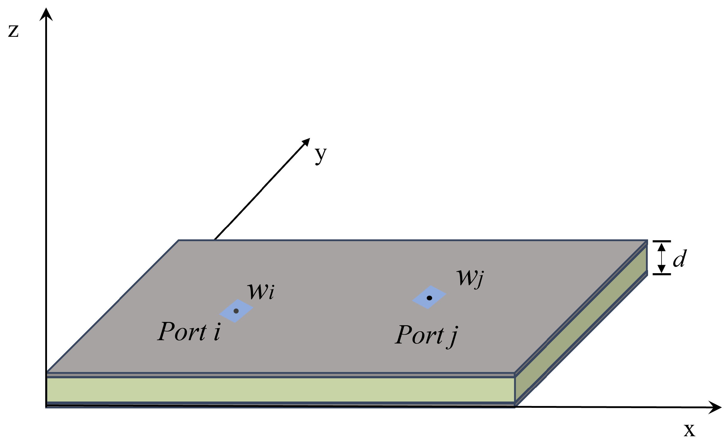
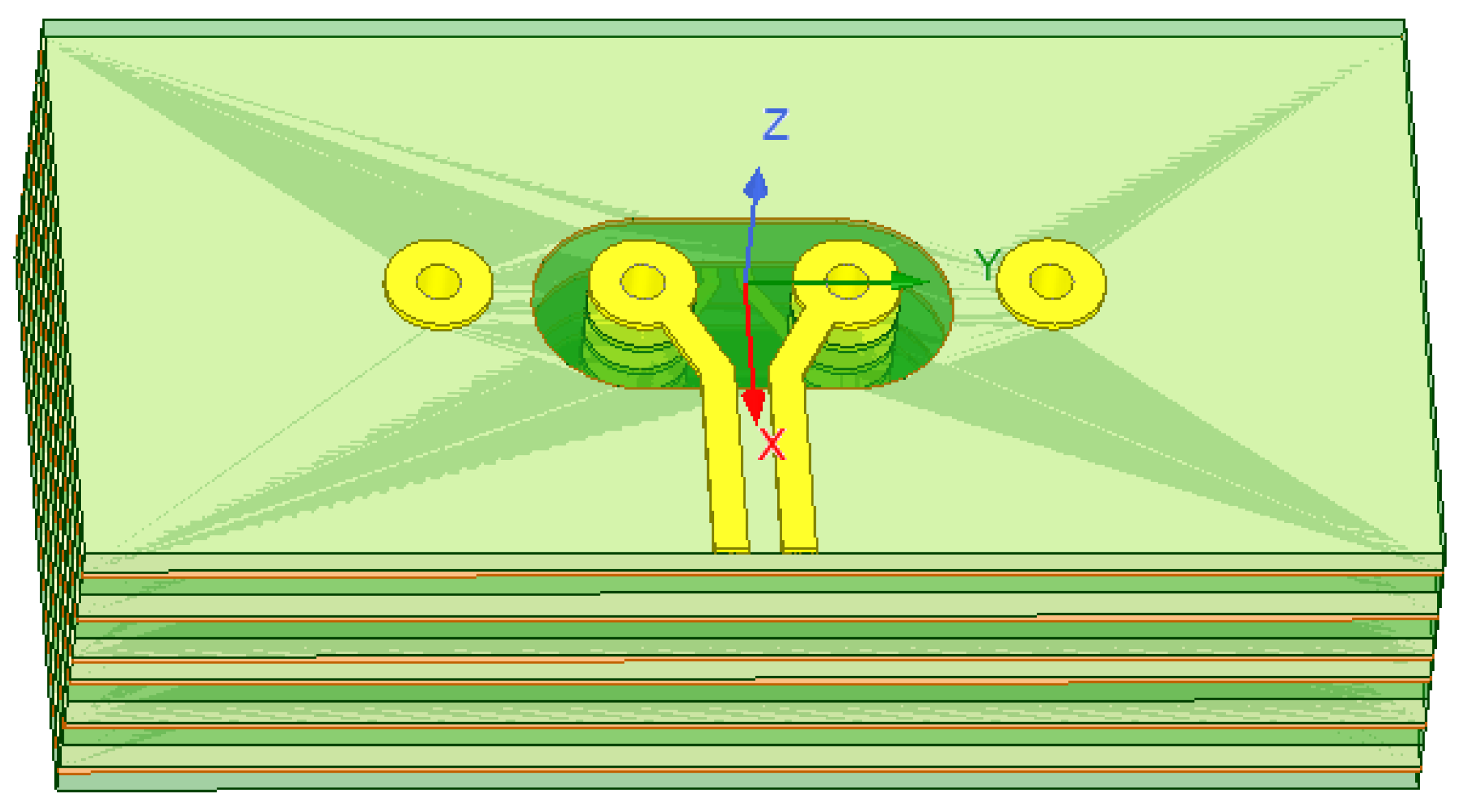
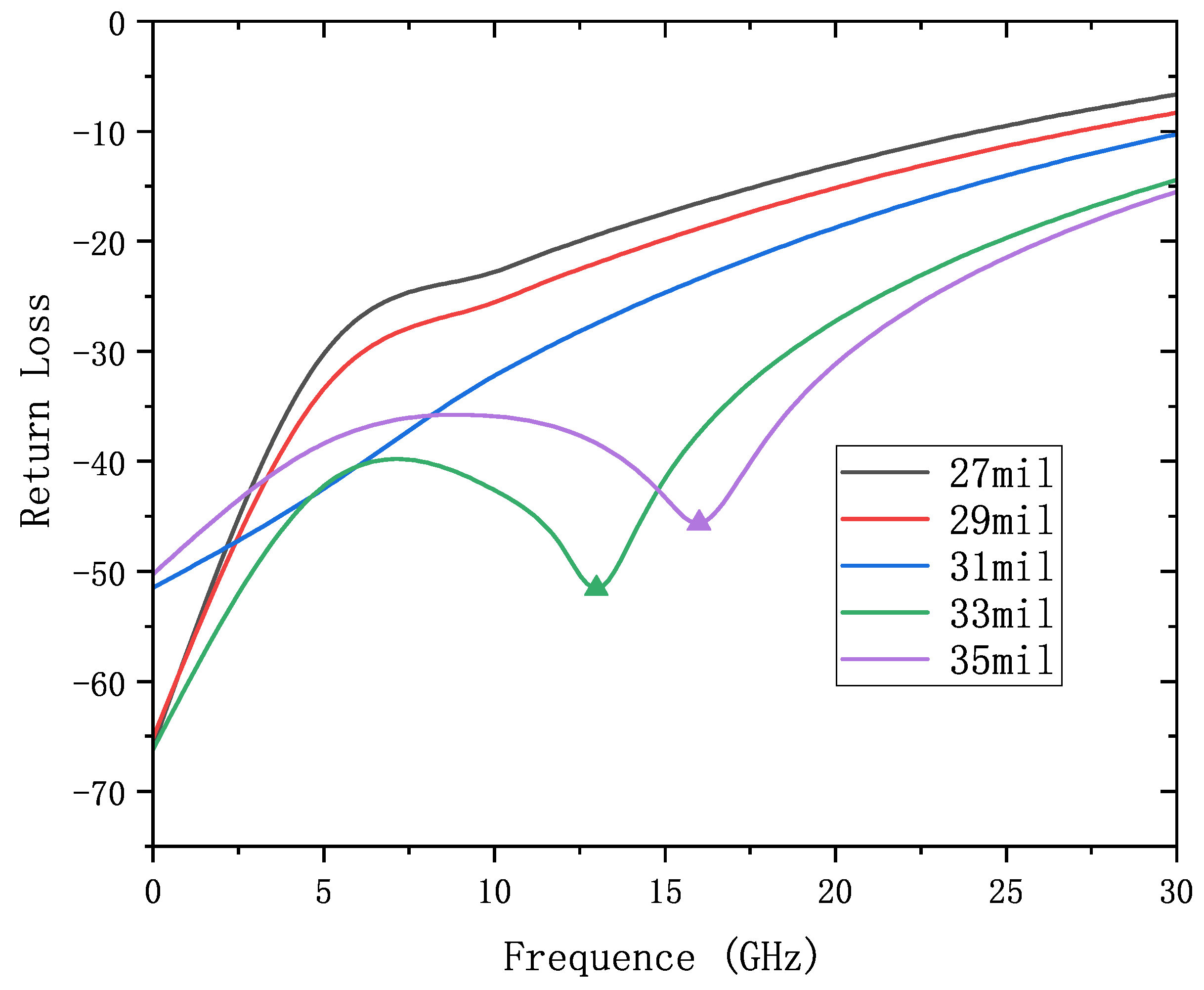
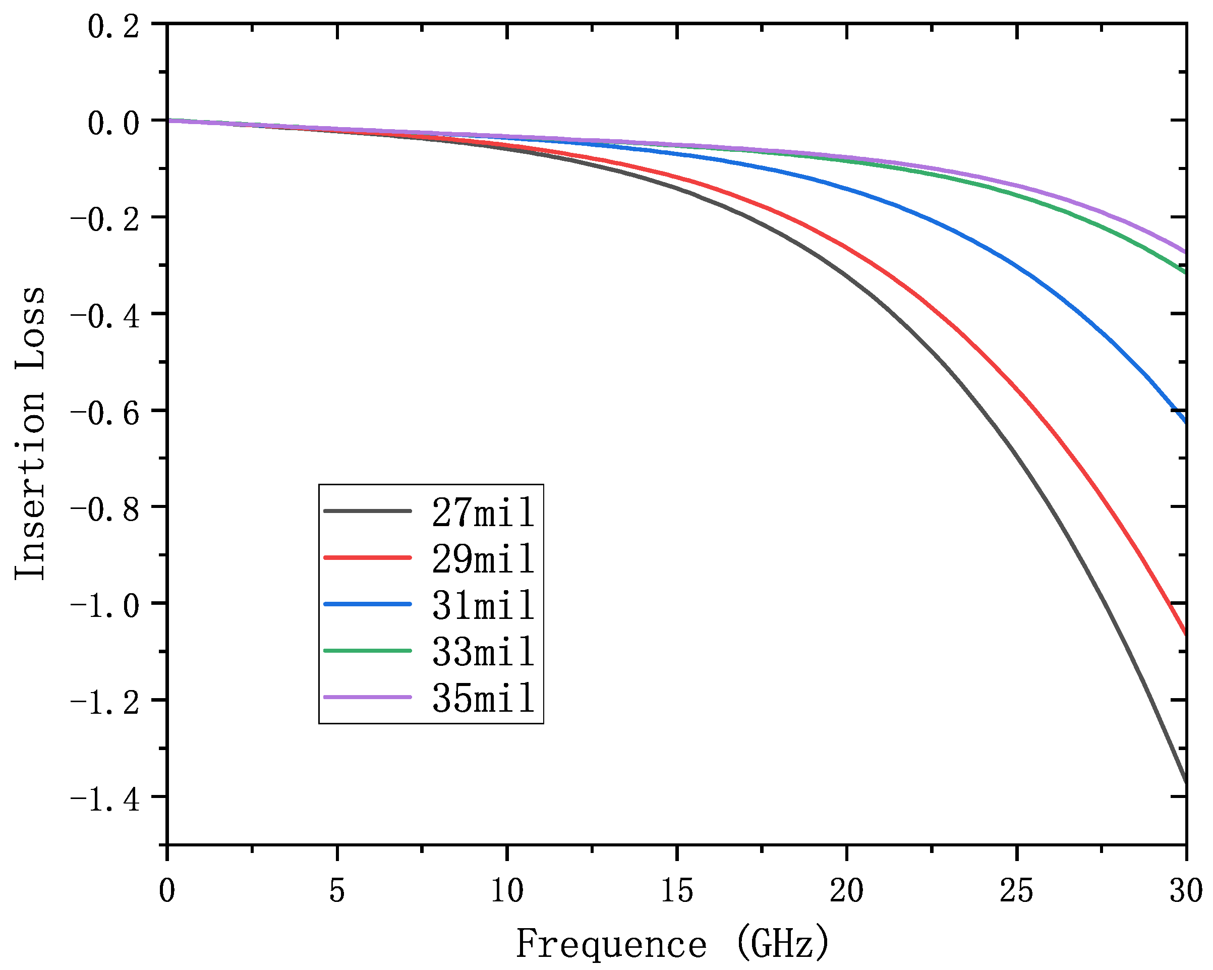

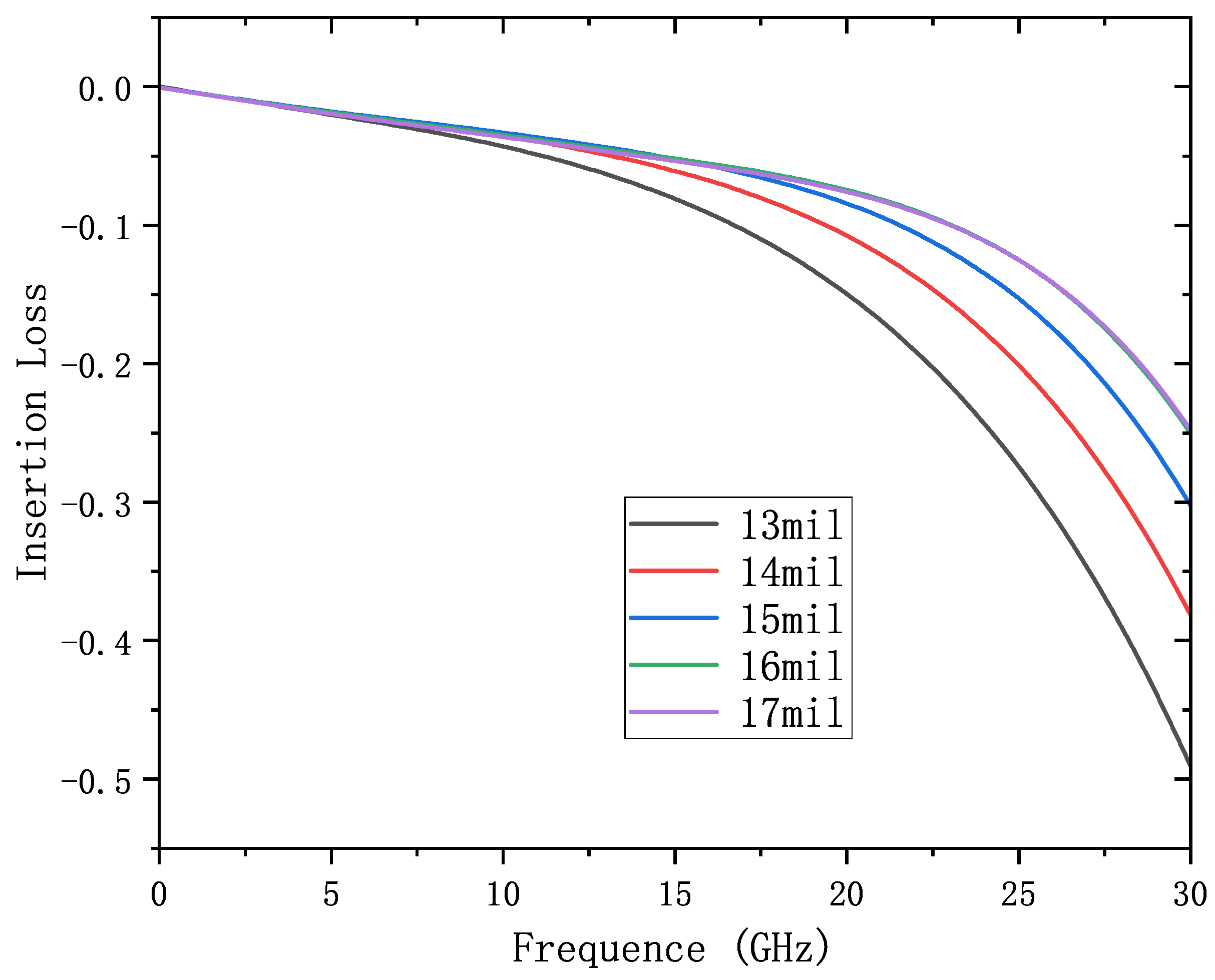

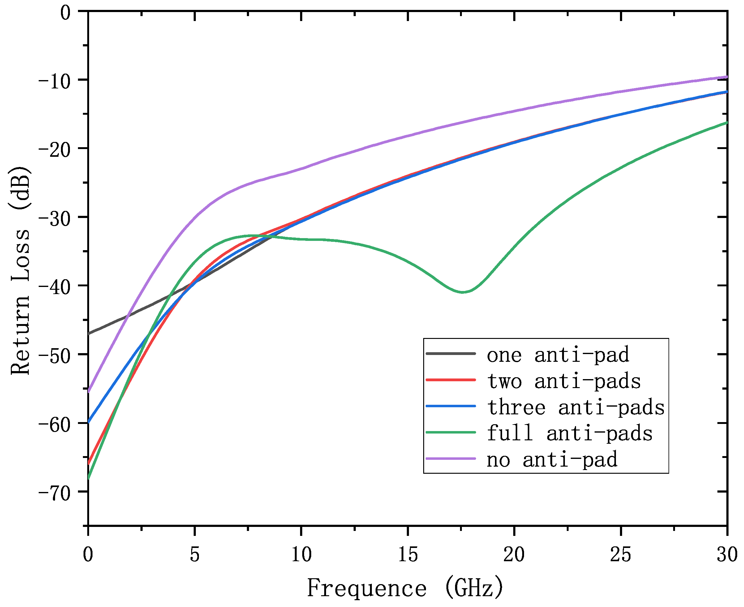
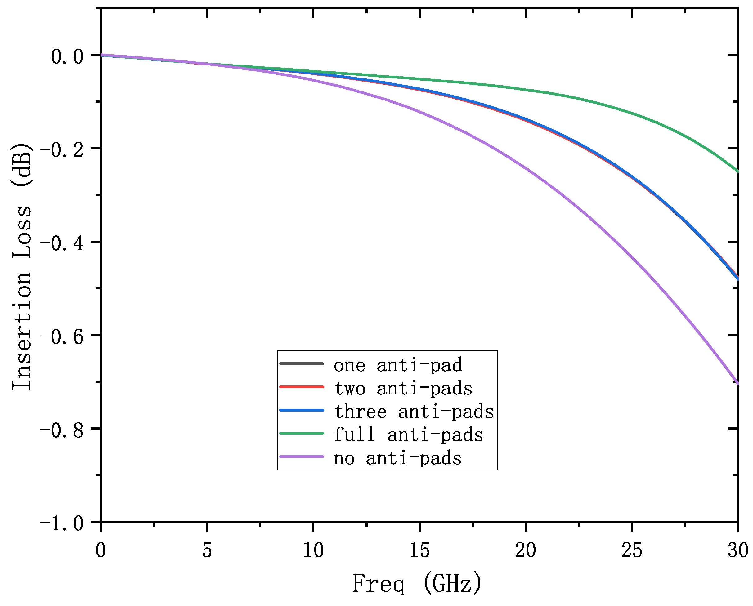


| Optimization Scheme | Measures Taken |
|---|---|
| Scheme 1 | The influence of the back-drill length on the S-parameter was investigated by keeping the VIA radius and anti-pad radius constant. |
| Scheme 2 | The influence of the anti-pad radius on the S-parameter was investigated by keeping the VIA radius and back-drill length constant. |
| Scheme 3 | On the basis of Scheme 1 and Scheme 2, the radius of the VIAs and anti-pads and the length of back-drill all remained unchanged, then anti-pads were added in the part troughed by the back-drill. The influence on the S-parameter was investigated. |
| Plane | Type |
|---|---|
| Layer 1/12 | Signal Plane |
| Layer 2/11 | Power Plane |
| Layer 3/10 | Signal Plane |
| Layer 4/9 | Power Plane |
| Layer 5/8 | Signal Plane |
| Layer 6/7 | Power Plane |
Disclaimer/Publisher’s Note: The statements, opinions and data contained in all publications are solely those of the individual author(s) and contributor(s) and not of MDPI and/or the editor(s). MDPI and/or the editor(s) disclaim responsibility for any injury to people or property resulting from any ideas, methods, instructions or products referred to in the content. |
© 2024 by the authors. Licensee MDPI, Basel, Switzerland. This article is an open access article distributed under the terms and conditions of the Creative Commons Attribution (CC BY) license (https://creativecommons.org/licenses/by/4.0/).
Share and Cite
Xu, W.-J.; Xin, D.-J.; Yang, L.; Zhou, Y.-K.; Wang, D.; Li, W.-X. High-Speed Signal Optimization at Differential VIAs in Multilayer Printed Circuit Boards. Electronics 2024, 13, 3377. https://doi.org/10.3390/electronics13173377
Xu W-J, Xin D-J, Yang L, Zhou Y-K, Wang D, Li W-X. High-Speed Signal Optimization at Differential VIAs in Multilayer Printed Circuit Boards. Electronics. 2024; 13(17):3377. https://doi.org/10.3390/electronics13173377
Chicago/Turabian StyleXu, Wen-Jie, Dong-Jin Xin, Lei Yang, Yong-Kang Zhou, Dong Wang, and Wei-Xin Li. 2024. "High-Speed Signal Optimization at Differential VIAs in Multilayer Printed Circuit Boards" Electronics 13, no. 17: 3377. https://doi.org/10.3390/electronics13173377
APA StyleXu, W.-J., Xin, D.-J., Yang, L., Zhou, Y.-K., Wang, D., & Li, W.-X. (2024). High-Speed Signal Optimization at Differential VIAs in Multilayer Printed Circuit Boards. Electronics, 13(17), 3377. https://doi.org/10.3390/electronics13173377


