
A Cryogenic 8-Bit 32 MS/s SAR ADC Operating down to 4.2 K


Abstract
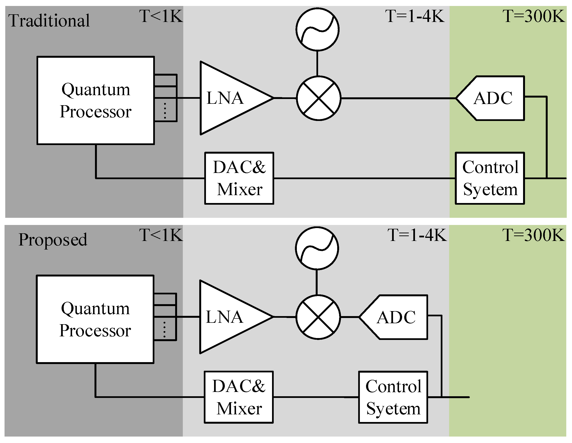
1. Introduction
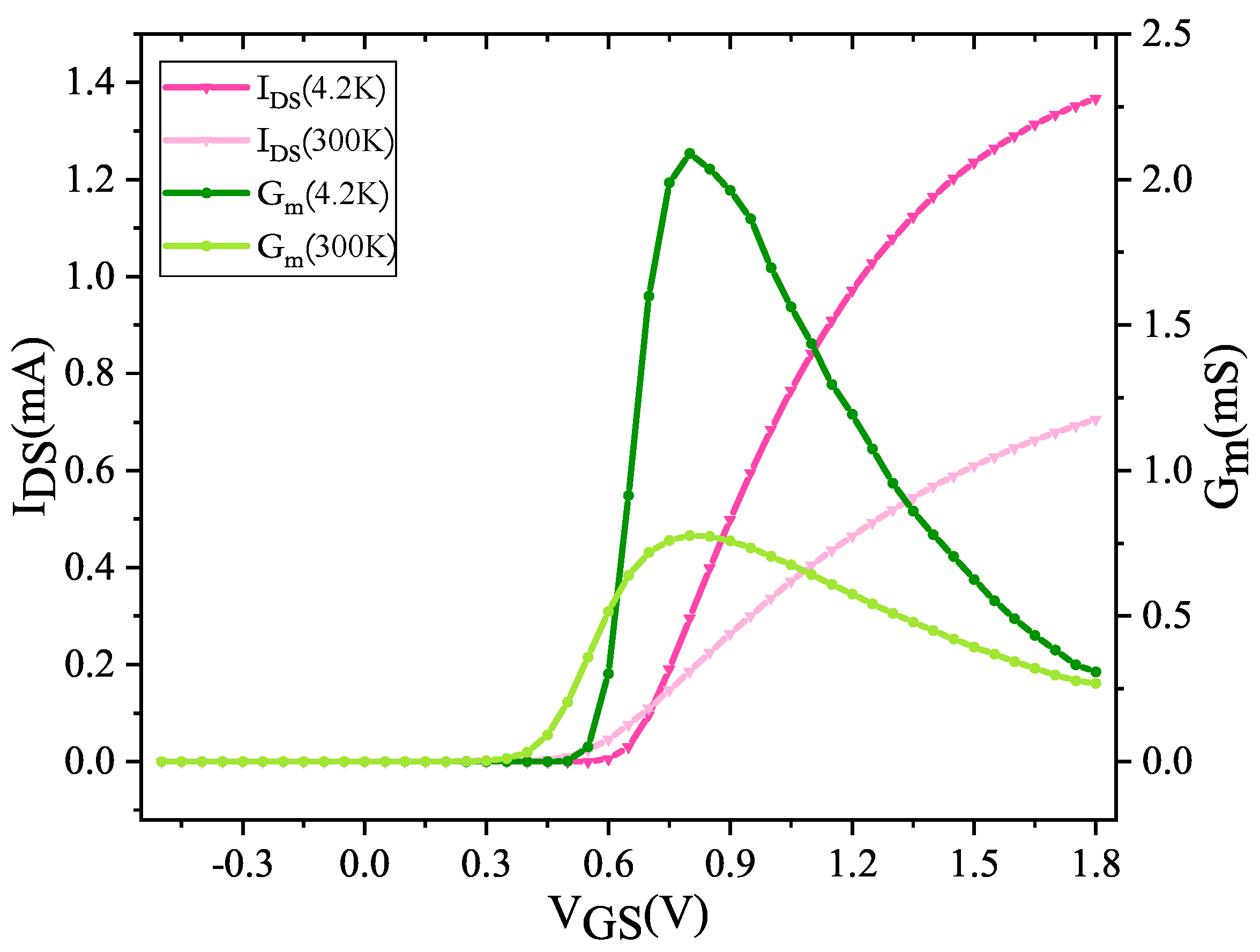
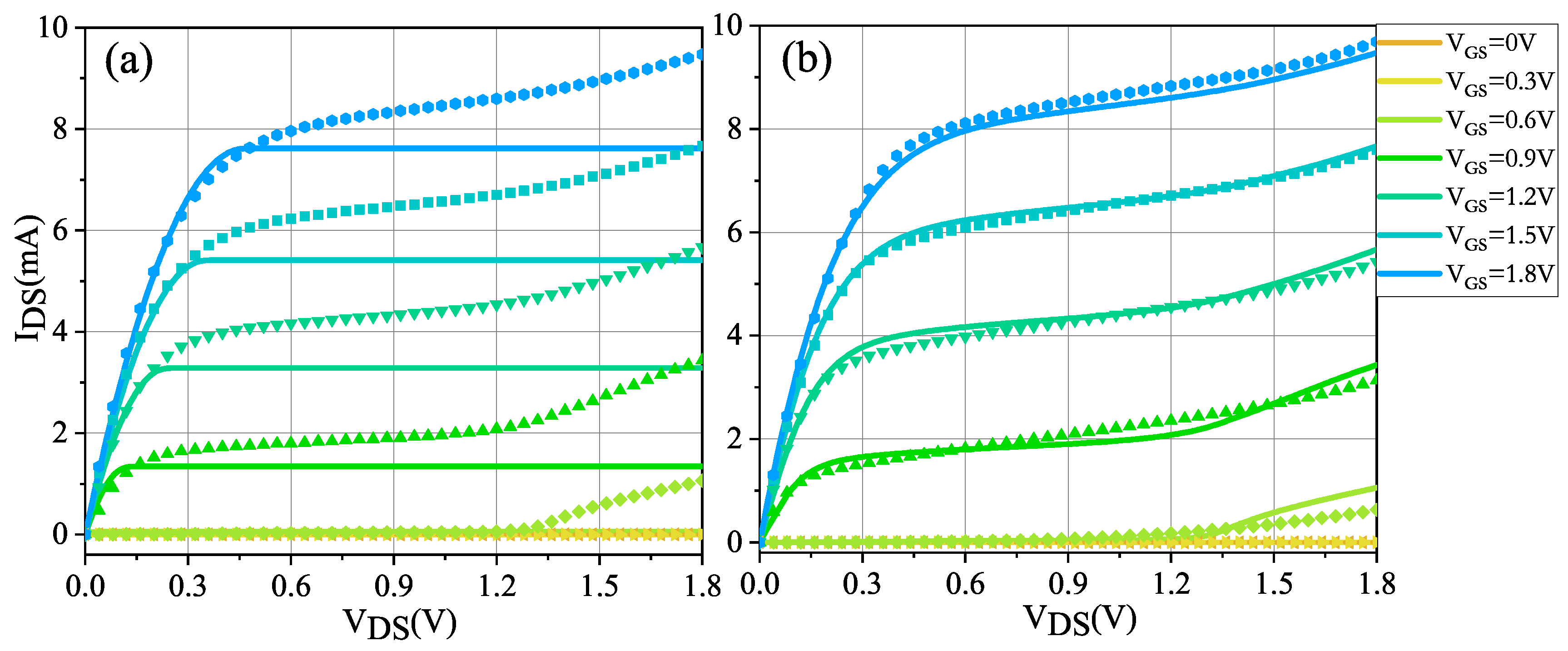
2. Cryogenic CMOS Characterization
3. Cryogenic SAR ADC
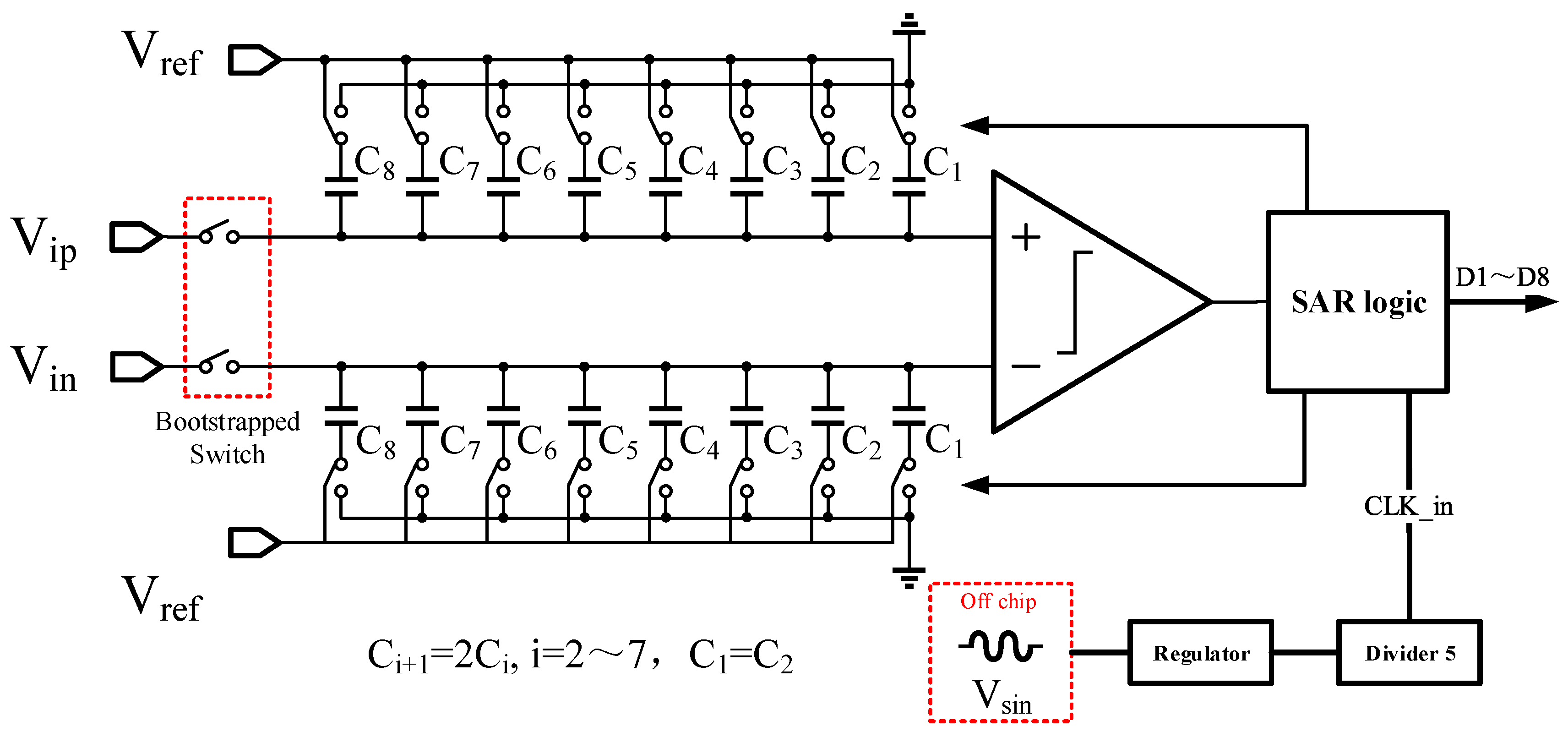
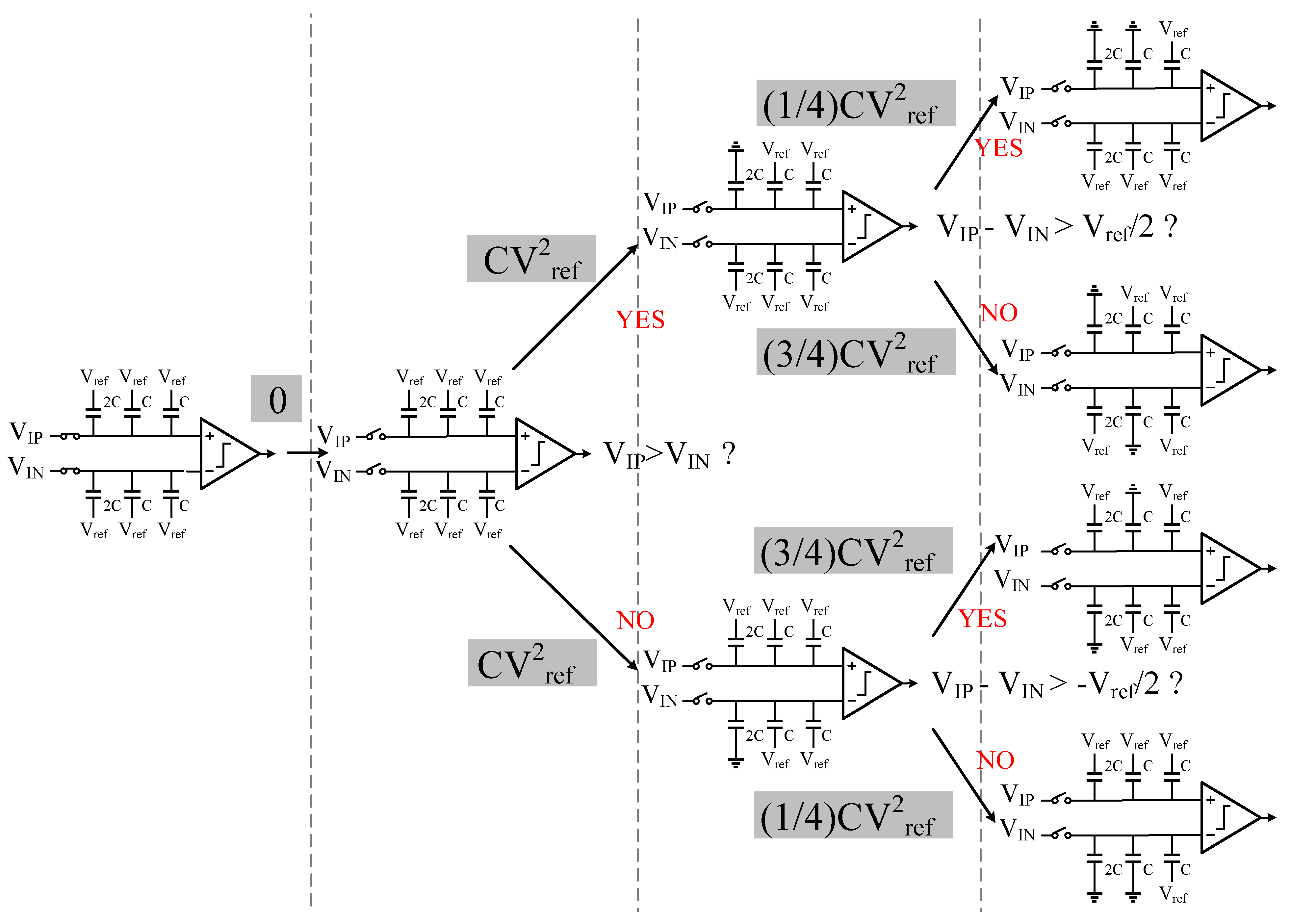
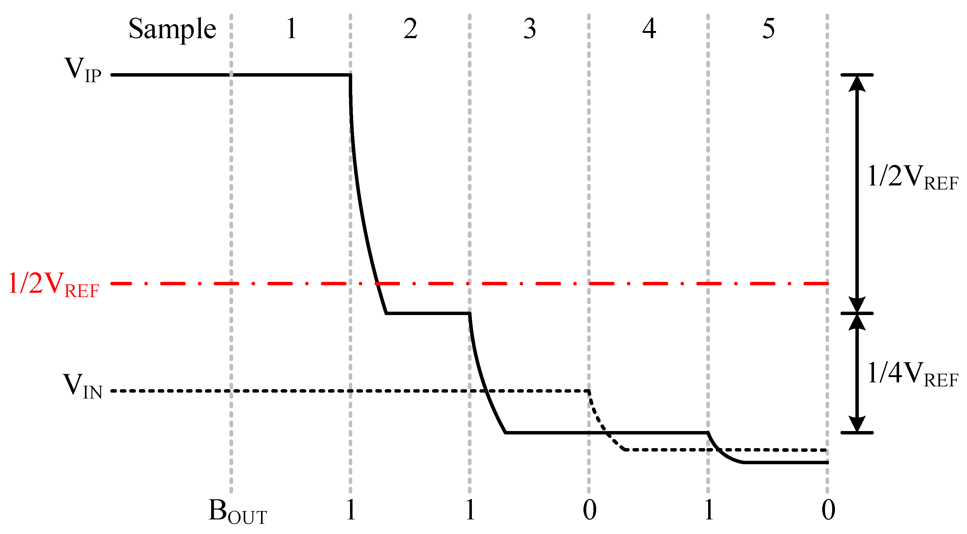
3.1. ADC Architecture
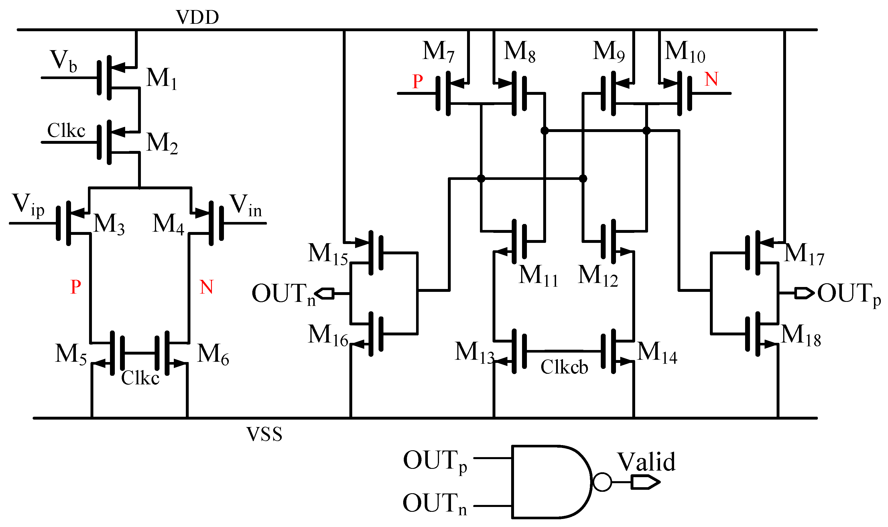
3.2. Dynamic Comparator
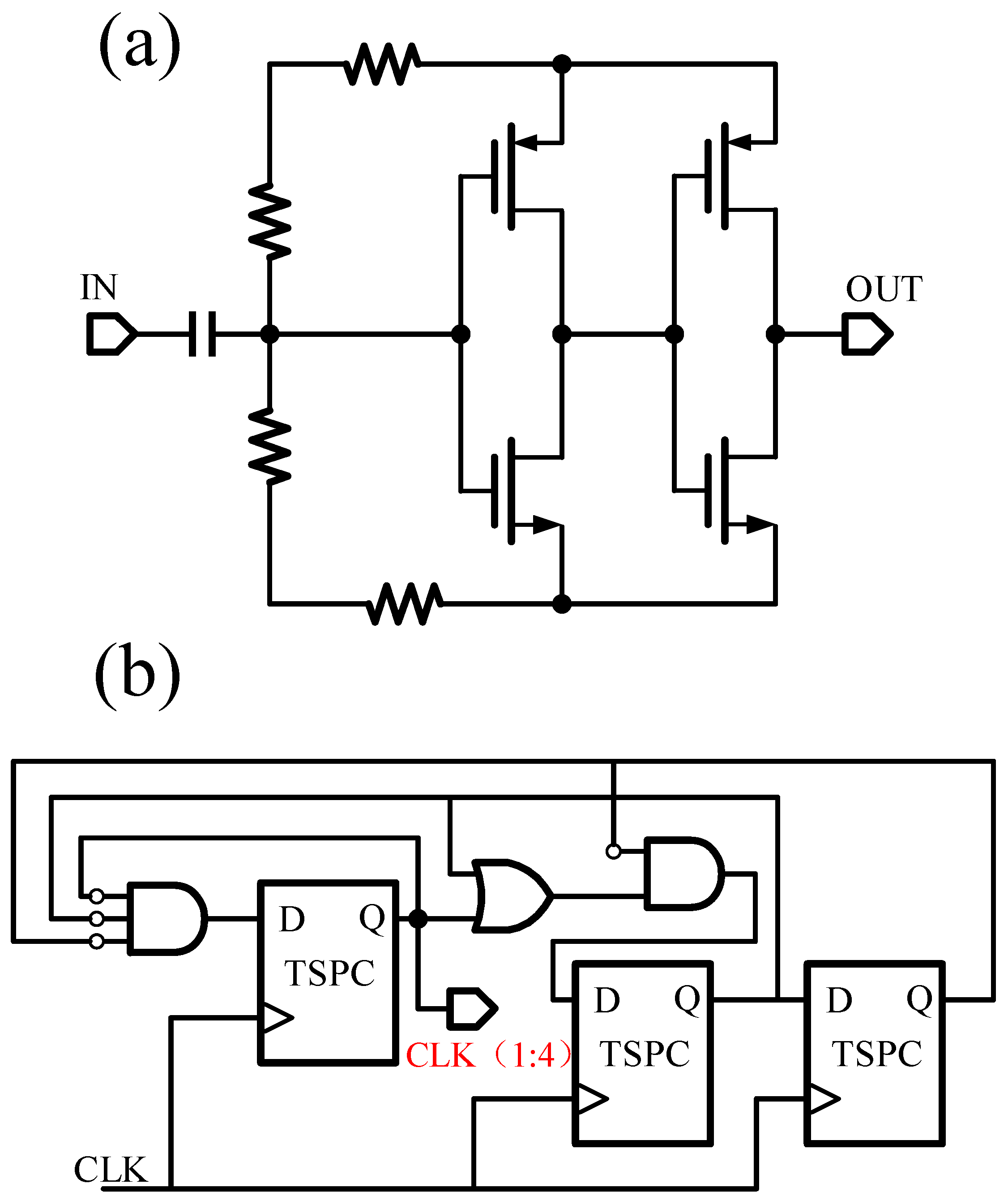
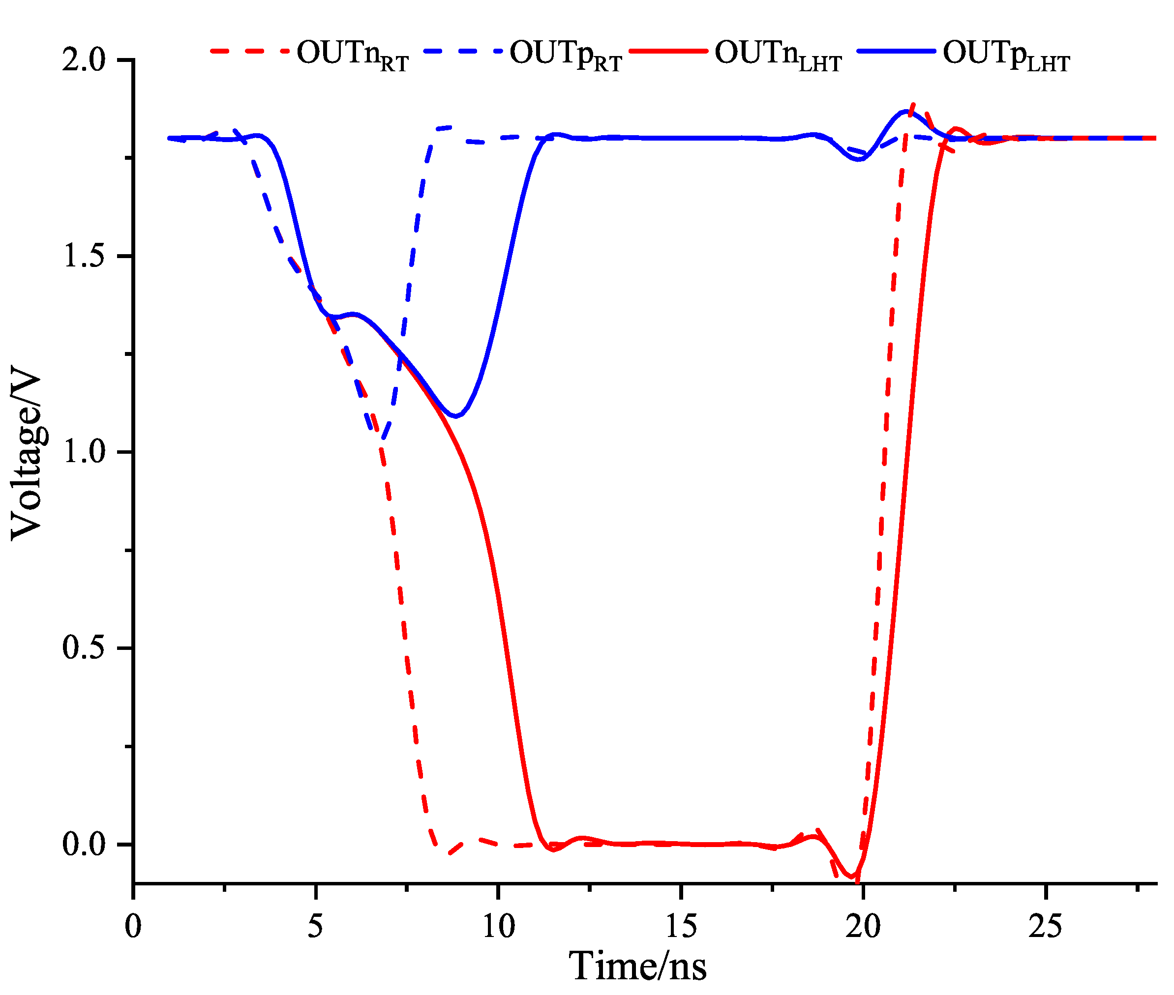
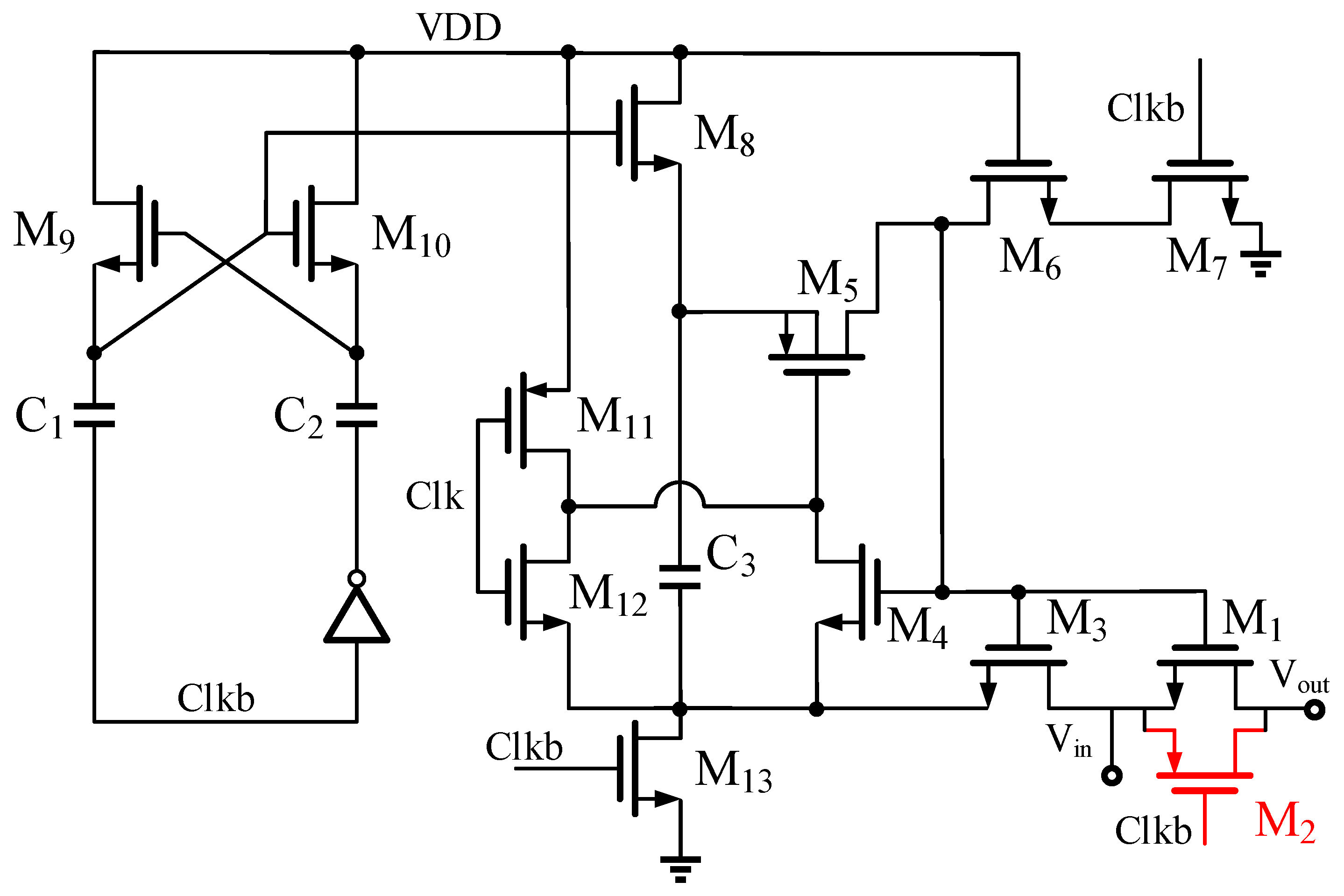
3.3. Bootstrapped Switch
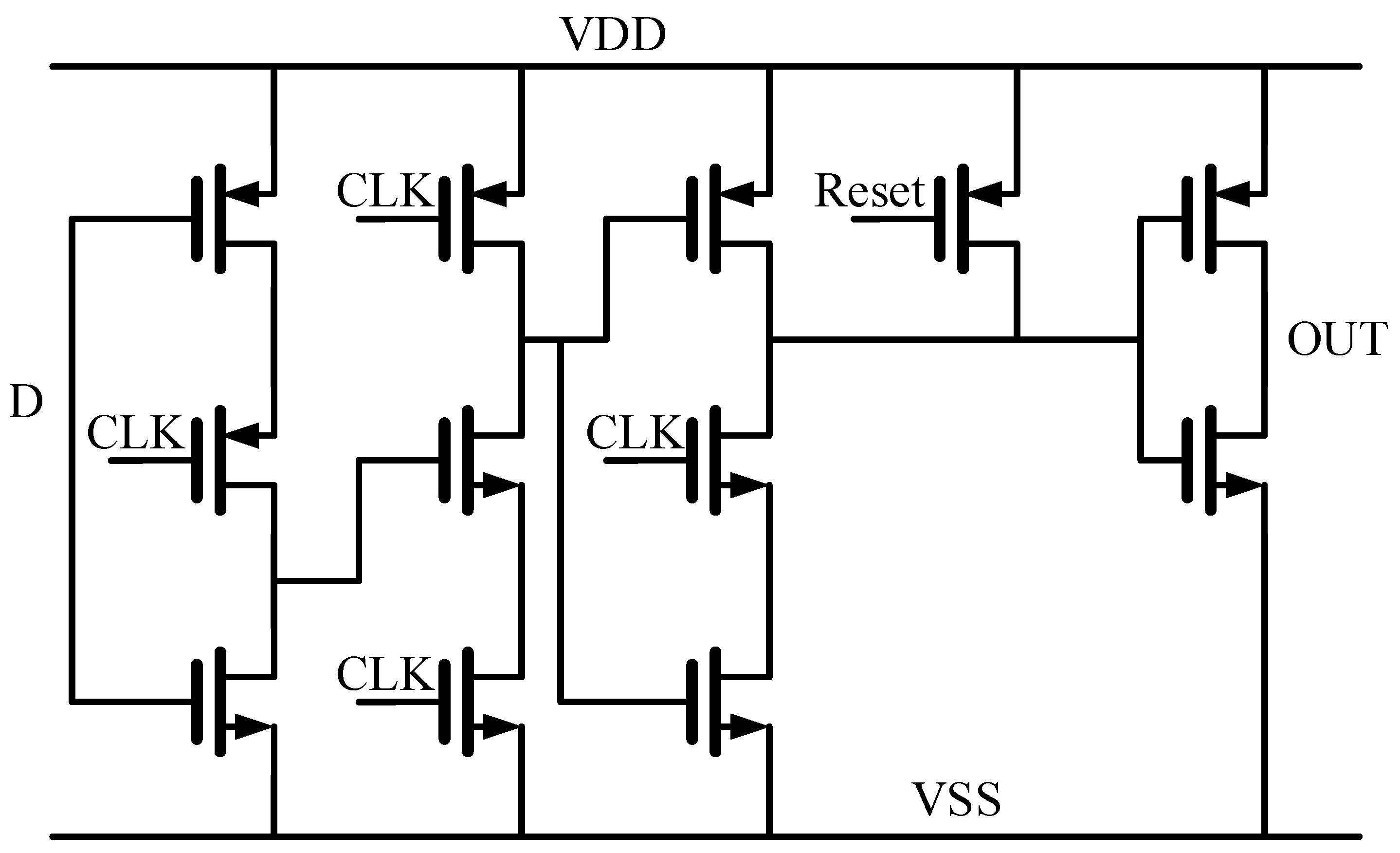
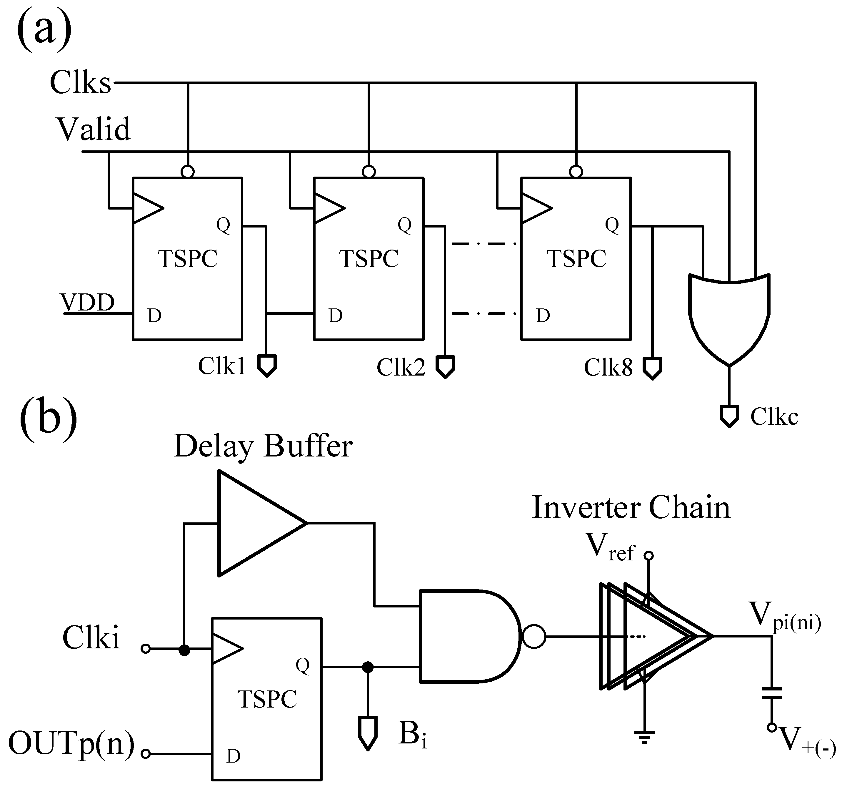
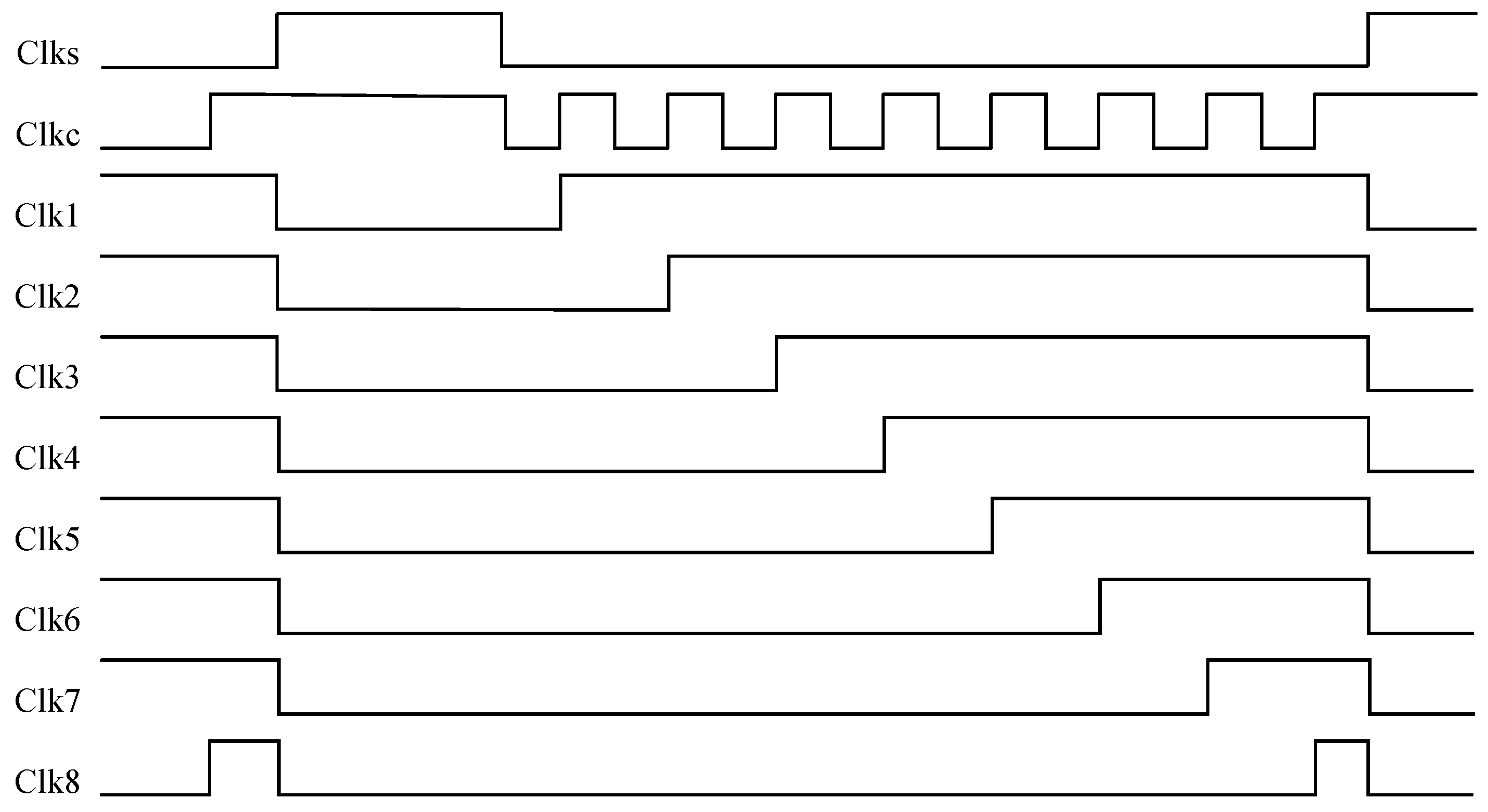
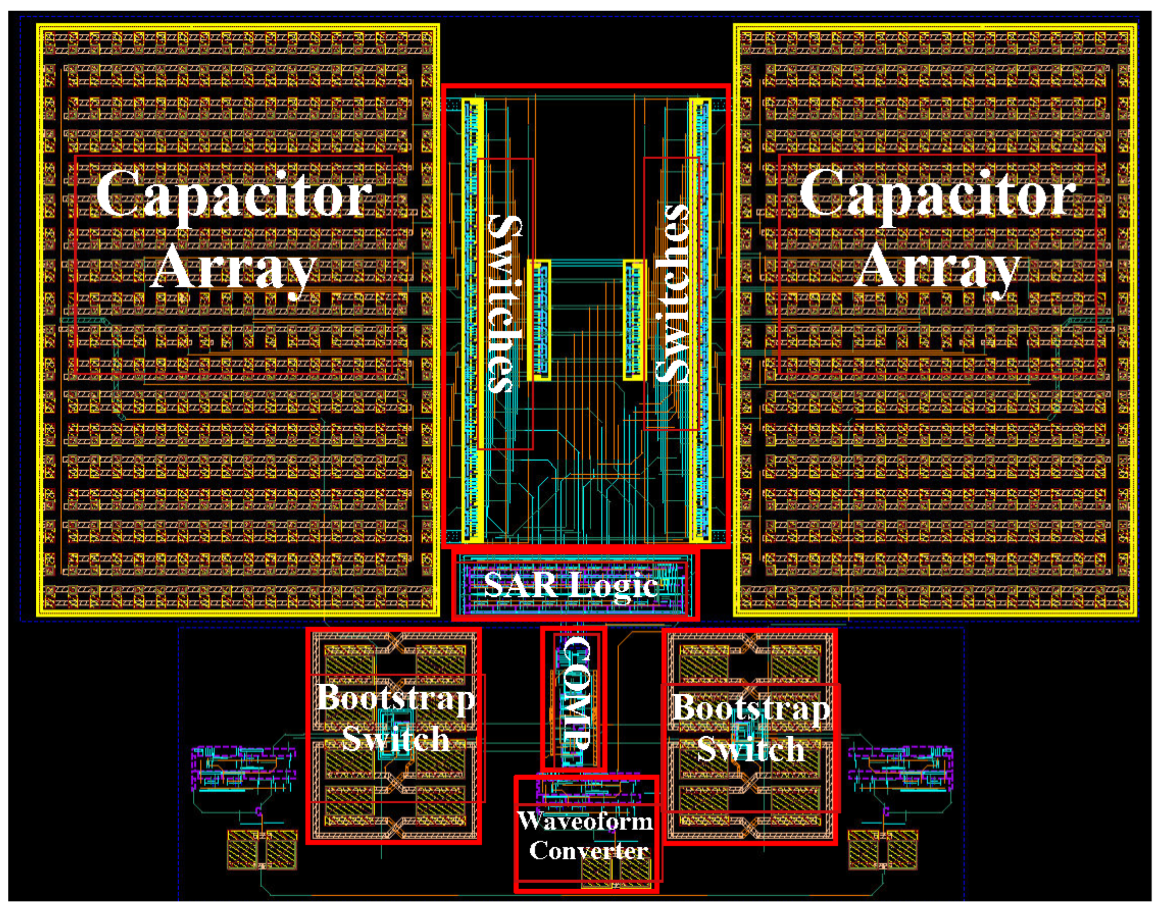
3.4. SAR Logic and Capacitor Array
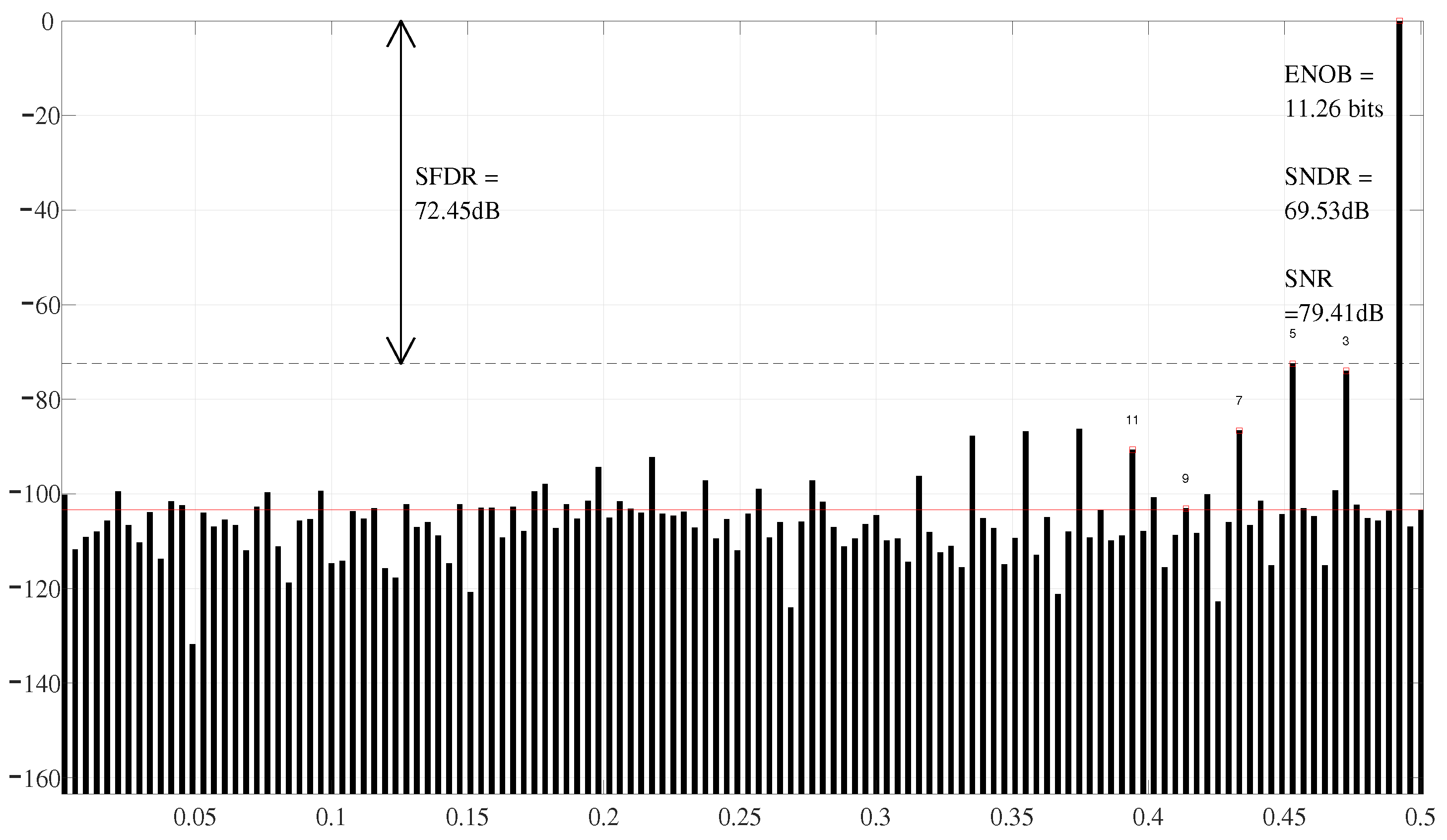
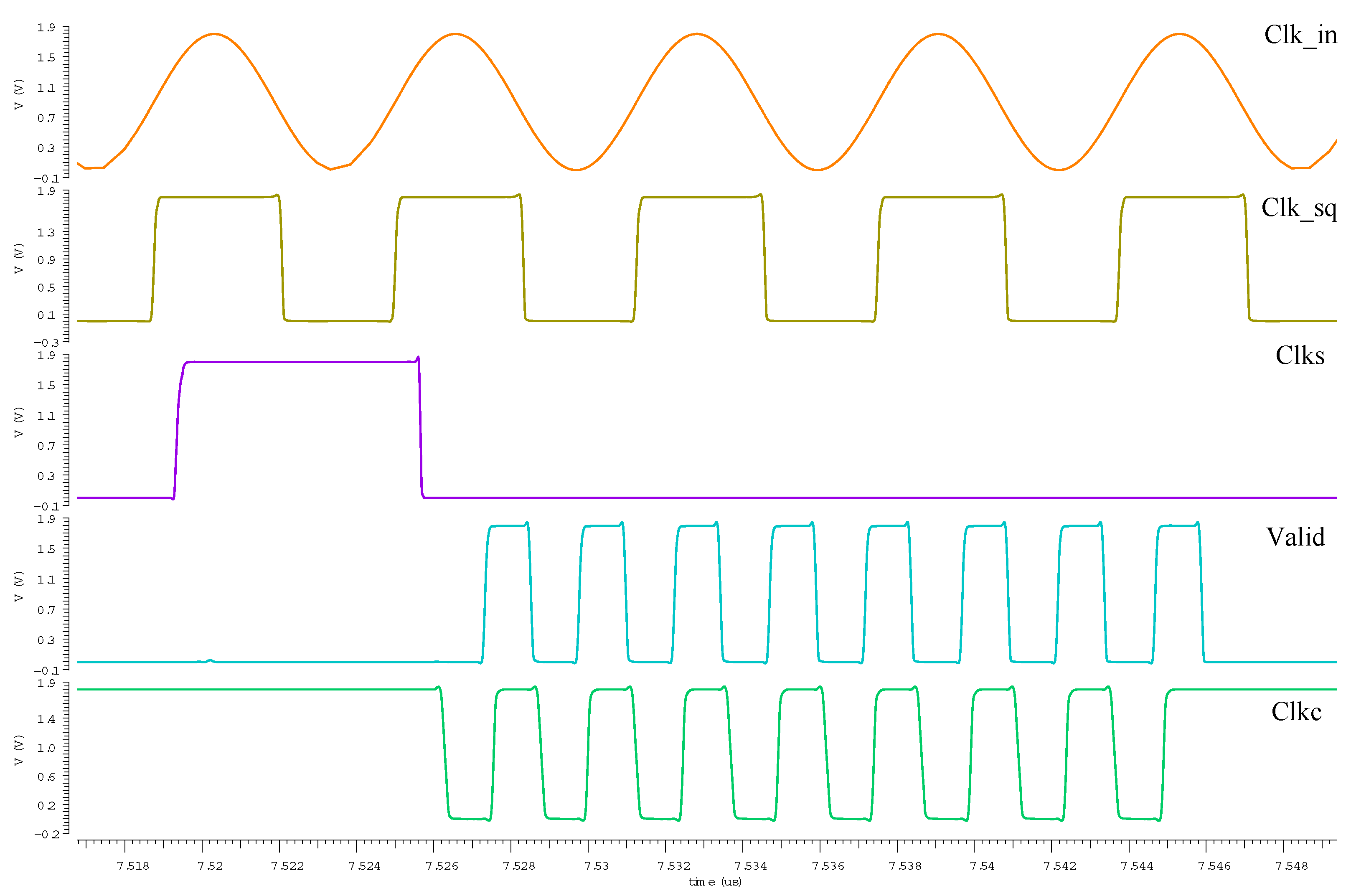
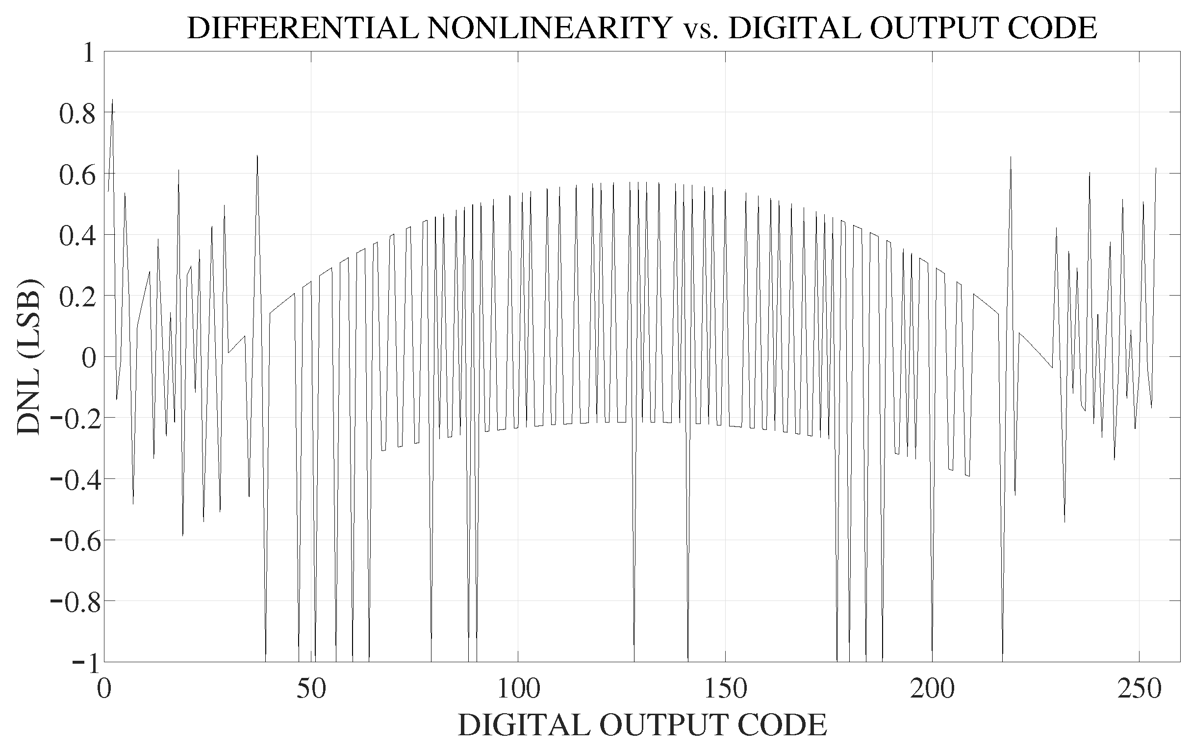
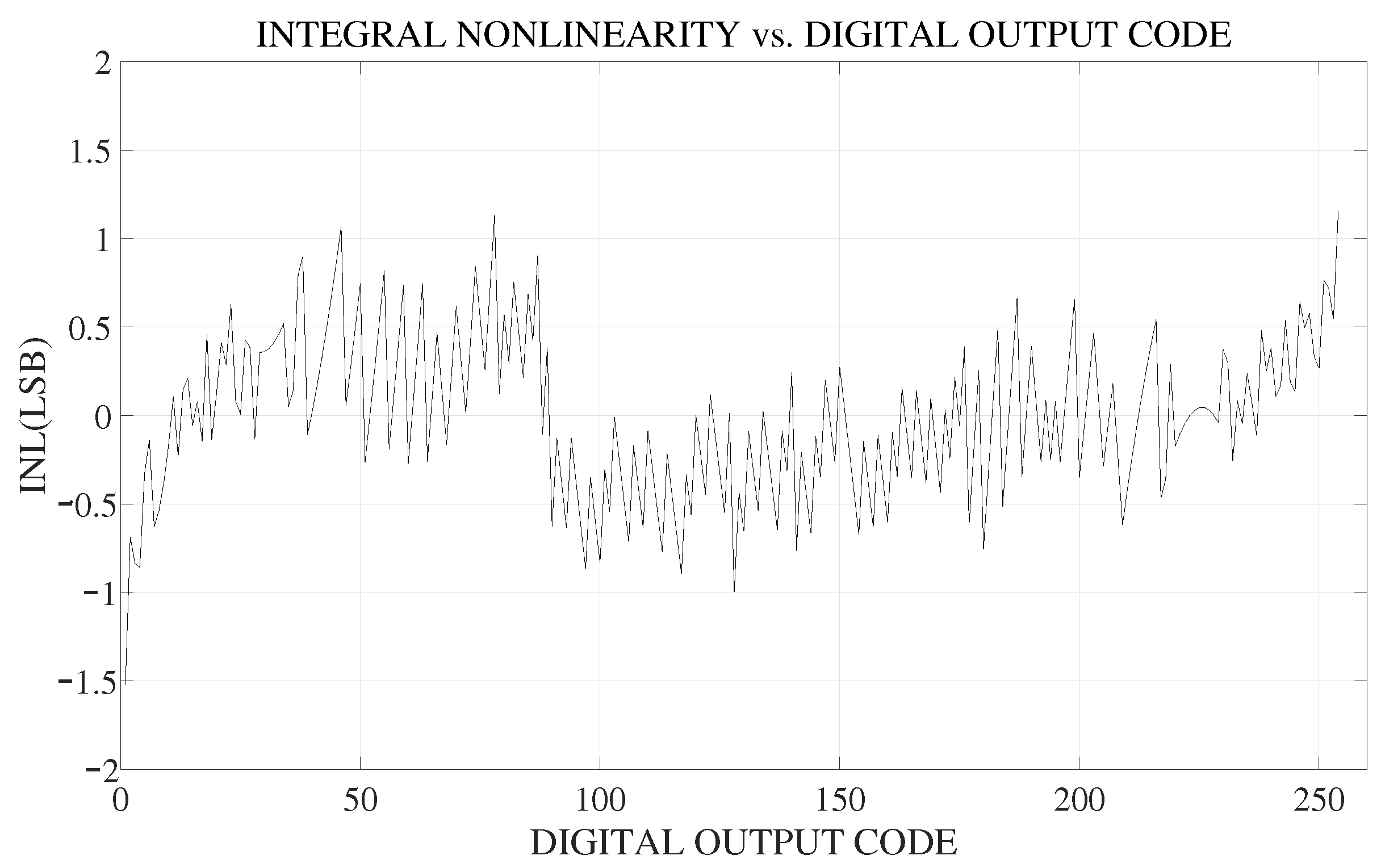
4. Simulation Results
5. Conclusions
Author Contributions
Funding
Data Availability Statement
Conflicts of Interest
Appendix A
References
- Zhu, Q.-L.; Cao, S.R.; Chen, F.S.; Peng, C.Z.; Zhu, X.B.; Pan, J.W. Quantum computational advantage via 60-qubit 24-cycle random circuit sampling. Sci. Bull. 2022, 3, 240–245. [Google Scholar] [CrossRef] [PubMed]
- Arute, F.; Arya, K.; Babbush, R.; Buell, D.A. Quantum supremacy using a programmable superconducting processor. Nature 2019, 7779, 505–510. [Google Scholar] [CrossRef] [PubMed]
- Gong, M.; Wang, S.Y.; Zhu, X.B.; Pan, J.W. Quantum walks on a programmable two-dimensional 62-qubit superconducting processor. Science 2021, 6545, 948–952. [Google Scholar] [CrossRef] [PubMed]
- Charbon, E.; Sebastiano, F.; Vladimirescu, A.; Homulle, H.; Visser, S.; Song, L.; Incandela, R.M. Cryo-CMOS for quantum computing. In Proceedings of the 2016 IEEE International Electron Devices Meeting, San Francisco, CA, USA, 12–18 December 2020. [Google Scholar]
- Bardin, J.C.; Jeffrey, E.; Lucero, E.; Huang, T.; Naaman, O.; Barends, R. A 28 nm Bulk-CMOS 4-to-8GHz ¡2mW Cryogenic Pulse Modulator for Scalable Quantum Computing. In Proceedings of the 2019 IEEE International Solid-State Circuits Conference, San Francisco, CA, USA, 17–21 February 2019. [Google Scholar]
- Patra, B.; Incandela, R.M.; van Dijk, J.P.G.; Homulle, H.A.R.; Sebastiano, F.; Charbon, E. Cryo-CMOS Circuits and Systems for Quantum Computing Applications. IEEE J. Solid-State Circuits 2018, 1, 309–321. [Google Scholar] [CrossRef]
- Charbon, E.; Sebastiano, F.; Babaie, M.; Valizadehpasha, B. Cryo-CMOS circuits and systems for scalable quantum computing. In Proceedings of the 2017 IEEE International Solid-State Circuits Conference, Austin, TX, USA, 18–22 June 2017. [Google Scholar]
- Sebastiano, F.; Homulle, H.A.R.; van Dijk, J.P.G.; Incandela, R.M.; Patra, B.; Charbon, E. Cryogenic CMOS interfaces for quantum devices. In Proceedings of the 2017 7th IEEE International Workshop on Advances in Sensors and Interfaces, Vieste, Italy, 15–16 June 2017. [Google Scholar]
- Liu, S.; Shen, Y.; Zhu, Z.M. A 12-Bit 10 MS/s SAR ADC With High Linearity and Energy-Efficient Switching. IEEE Trans. Circuits Syst. I Reg. Pap 2016, 10, 1616–1627. [Google Scholar] [CrossRef]
- Kim, W.; Hong, H.K.; Roh, Y.J.; Kang, H.W.; Ryu, S.T. A 0.6 V 12 b 10 MS/s Low-Noise Asynchronous SAR-Assisted Time-Interleaved SAR (SATI-SAR) ADC. IEEE J. Solid-State Circuits 2016, 8, 1826–1839. [Google Scholar] [CrossRef]
- Lee, S.; Chandrakasan, A.P.; Lee, H.S. A 1 GS/s 10b 18.9 mW Time-Interleaved SAR ADC With Background Timing Skew Calibration. IEEE J. Solid-State Circuits 2014, 12, 2846–2856. [Google Scholar] [CrossRef]
- Xie, Y.; Liang, Y.H.; Liu, M.L.; Liu, S.B.; Zhu, Z.M. A 10-Bit 5 MS/s VCO-SAR ADC in 0.18-μm CMOS. IEEE Trans. Circuits Syst. II Express Briefs 2019, 1, 26–30. [Google Scholar]
- Creten, Y.; Merken, P.; Sansen, W.; Mertens, R.; van Hoof, C. A Cryogenic ADC operating Down to 4.2K. In Proceedings of the 2007 IEEE International Solid-State Circuits Conference, San Francisco, CA, USA, 11–15 February 2007. [Google Scholar]
- Kiene, G.; Catania, A.; Overwater, R.; Bruschi, P.; Charbon, E.; Babaie, M.; Sebastiano, F.; Valizadehpasha, B. A 1GS/s 6-to-8b 0.5 mW/Qubit Cryo-CMOS SAR ADC for Quantum Computing in 40 nm CMOS. In Proceedings of the 2021 IEEE International Solid-State Circuits Conference, San Francisco, CA, USA, 13–22 February 2021. [Google Scholar]
- Incandela, R.M.; Song, L.; Homulle, H.; Charbon, E.; Vladimirescu, A.; Sebastiano, F. Characterization and Compact Modeling of Nanometer CMOS Transistors at Deep-Cryogenic Temperatures. IEEE J. Electron. Devices Soc. 2018, 1, 996–1006. [Google Scholar] [CrossRef]
- Luo, C.; Li, Z.; Lu, T.T.; Xu, J.; Guo, G.P. MOSFET characterization and modeling at cryogenic temperatures. Cryogenics 2019, 98, 12–17. [Google Scholar] [CrossRef]
- Hafez, I.M.; Ghibaudo, G.; Balestra, F. Reduction of kink effect in short-channel MOS transistors. IEEE Electron. Device Lett. 1990, 3, 120–122. [Google Scholar] [CrossRef]
- Li, Z.; Luo, C.; Lu, T.T.; Xu, J.; Kong, W.C.; Guo, G.P. Modelling and kink correction of 0.18 μm bulk CMOS at liquid helium temperature. Electron. Lett. 2019, 14, 780–783. [Google Scholar] [CrossRef]
- Chen, H.-C.; Huang, S.P.; Chang, T.C. Inhibiting the Kink Effect and Hot-Carrier Stress Degradation Using Dual-Gate Low-Temperature Poly-Si TFTs. IEEE Electron. Device Lett. 2020, 1, 54–57. [Google Scholar] [CrossRef]
- ’t Hart, P.A.; van Dijk, J.P.G.; Babaie, M.; Charbon, E.; Vladimircscu, A.; Sebastiano, F. Characterization and Model Validation of Mismatch in Nanometer CMOS at Cryogenic Temperatures. In Proceedings of the 2018 48TH European Solid-State Device Research Conference, Dresden, Germany, 3–6 September 2018. [Google Scholar]
- Huang, Y.; Luo, C.; Lu, T.T.; Guo, G.P. A cryogenic low power CMOS analog buffer at 4.2K. IEICE Electron. Express 2021, 12, 1–5. [Google Scholar] [CrossRef]
- Wu, C.; Yuan, J. A 12-Bit, 300-MS/s Single-Channel Pipelined-SAR ADC With an Open-Loop MDAC. IEEE J. Solid-State Circuits 2019, 5, 1446–1454. [Google Scholar] [CrossRef]
- Xu, Z.; Hu, B.; Wu, T.X.; Ma, S.L. A 12-Bit 50 MS/s Split-CDAC-Based SAR ADC Integrating Input Programmable Gain Amplifier and Reference Voltage Buffer. Electronics 2022, 12, 1841. [Google Scholar] [CrossRef]
- Zheng, Y.; Ye, F.; Ren, J.Y. A 12-Bit, 100 MS/s SAR ADC Based on a Bridge Capacitor Array with Redundancy and Non-Linearity Calibration in 28 nm CMOS. Electronics 2022, 5, 705. [Google Scholar] [CrossRef]
- Ramkaj, A.T.; Strackx, M.; Steyaert, M.S.J.; Tavernier, F. A 1.25-GS/s 7-b SAR ADC With 36.4-dB SNDR at 5 GHz Using Switch-Bootstrapping, USPC DAC and Triple-Tail Comparator in 28-nm CMOS. IEEE J. Solid-State Circuits 2018, 7, 1889–1901. [Google Scholar] [CrossRef]
- Liu, C.-C.; Chang, S.J.; Huang, G.Y.; Lin, Y.Z. A 10-bit 50-MS/s SAR ADC With a Monotonic Capacitor Switching Procedure. IEEE J. Solid-State Circuits 2010, 4, 731–740. [Google Scholar] [CrossRef]
- Chevella, S.; Catania, A.; Sebastiano, F. A Low-Power 1-V Supply Dynamic Comparator. IEEE Solid State Circuits Lett. 2020, 3, 154–157. [Google Scholar] [CrossRef]
- Van Elzakker, M.; Nauta, B. A 10-bit Charge-Redistribution ADC Consuming 1.9 mu W at 1 MS/s. IEEE J. Solid-State Circuits 2010, 5, 1007–1015. [Google Scholar] [CrossRef]
- Aksin, D.; Al-Shyoukh, M.; Maloberti, F. Switch Bootstrapping for Precise Sampling Beyond Supply Voltage. IEEE J. Solid-State Circuits 2006, 8, 1938–1943. [Google Scholar] [CrossRef]
- Abo, A.M.; Gray, P.R. A 1.5-V, 10-bit, 14.3-MS/s CMOS Pipeline Analog-to-Digital Converter. IEEE J. Solid-State Circuits 1999, 5, 599–606. [Google Scholar] [CrossRef]
- Histogram Testing Determines DNL and INL Errors. Available online: https://www.analog.com/en/technical-articles/histogram-testing-determines-dnl-and-inl-errors.html (accessed on 8 July 2022).
- Verma, D.; Shehzad, K.; Khan, D.; Kim, S.J.; Pu, Y.G.; Yoo, S.-S.; Hwang, K.C.; Yang, Y.; Lee, K.-Y. A Design of Low-Power 10-bit 1-MS/s Asynchronous SAR ADC for DSRC Application. Electronics 2020, 9, 1100. [Google Scholar] [CrossRef]


| This Work | [14] | [13] | |
|---|---|---|---|
| Architecture | SAR | TI SAR | SAR |
| Technology | 180 nm | 40 nm | 0.7 m |
| Sample frequency | 32 MS/s | 1 GS/s | 3 kS/s |
| Supply voltage | 1.8 V | 1.1 V | 5 V |
| Input range () | 1.7 V | 0.7 V | 5 V |
| SNDR@Nyquist | 47.7 dB | 36.2 dB | - |
| SFDR@Nyquist | 54.53 dB | 48.5 dB | - |
| Power | 2.4 mW | 10.6 mW | 0.35 mW |
| FoM | 378 fJ/Conv.-step | 200 fJ/Conv.-step | - |
Disclaimer/Publisher’s Note: The statements, opinions and data contained in all publications are solely those of the individual author(s) and contributor(s) and not of MDPI and/or the editor(s). MDPI and/or the editor(s) disclaim responsibility for any injury to people or property resulting from any ideas, methods, instructions or products referred to in the content. |
© 2023 by the authors. Licensee MDPI, Basel, Switzerland. This article is an open access article distributed under the terms and conditions of the Creative Commons Attribution (CC BY) license (https://creativecommons.org/licenses/by/4.0/).
Share and Cite
Huang, Y.; Luo, C.; Guo, G. A Cryogenic 8-Bit 32 MS/s SAR ADC Operating down to 4.2 K. Electronics 2023, 12, 1420. https://doi.org/10.3390/electronics12061420
Huang Y, Luo C, Guo G. A Cryogenic 8-Bit 32 MS/s SAR ADC Operating down to 4.2 K. Electronics. 2023; 12(6):1420. https://doi.org/10.3390/electronics12061420
Chicago/Turabian StyleHuang, Yajie, Chao Luo, and Guoping Guo. 2023. "A Cryogenic 8-Bit 32 MS/s SAR ADC Operating down to 4.2 K" Electronics 12, no. 6: 1420. https://doi.org/10.3390/electronics12061420
APA StyleHuang, Y., Luo, C., & Guo, G. (2023). A Cryogenic 8-Bit 32 MS/s SAR ADC Operating down to 4.2 K. Electronics, 12(6), 1420. https://doi.org/10.3390/electronics12061420