1. Introduction
With the increasing functions and performance of satellite systems, the volume and weight of their microwave systems have also increased significantly, which has become a bottleneck restricting the development of payloads. Therefore, on the basis of ensuring high reliability, reductions in weight and improvements in the integration of microwave systems are urgently needed. The surface-mounted package used in the traditional space-borne microwave system is planar integration; the pin frequency is limited, the square shell shape is not conducive to cavity separation, and the matching restriction of thermal expansion coefficient limits the system integration of a large number of microwave dies [
1,
2,
3,
4]. With the development of special substrate materials such as silicon-based and laminated fabrication technology, system-level encapsulated microwave components based on wafers, substrates with three-dimensional (3D) heterogeneous integration, have been developed [
5,
6,
7,
8]. However, they are usually limited by their internal microwave interconnection structures, and their application frequencies cannot be further expanded. On the other hand, their interconnection structure is not reliable enough to meet the requirements of airtightness, severe changes of temperature, and changes of mechanical stress in space-borne applications. It is difficult to realize 3D integration and high reliability at the same time [
9,
10].
In this paper, a new method of space-borne microwave metallic system-in-package (SIP) based on highly reliable microwave interconnection is presented. This method uses metal airtight encapsulation and a novel gradient coaxial structure combined with microstrip impedance transformation and gold-ribbon interconnection to realize the horizontal and vertical interconnection of microwave signals. At the same time, it has thermal deformation resistance and excellent microwave transmission characteristics. Complex microwave circuits are divided into 3D layouts, thus achieving the 3D distribution of the horizontal and vertical directions of the microwave circuits’ cavity. By simulating and calculating the microwave characteristics of various highly reliable interconnections, a microwave transition structure with excellent microwave characteristics is proposed, and its design dimensions are derived. Its microwave transmission frequency can cover DC-40 GHz. The space-borne microwave SIP based on the novel interconnection can achieve airtight characteristics, temperature changes, and mechanical adaptability. Finally, a 3D SIP with high reliability that can adapt to the application of aerospace products is designed and manufactured, which has excellent microwave characteristics.
2. Analysis of Traditional Interconnections in Space-Borne Microwave Systems
The microwave transceiver is the core part of all kinds of space-borne microwave equipment and also the most complex circuit part. It can realize microwave signal reception, amplification, filtering, frequency conversion, and specific gain or temperature regulation functions. There are many functional components and circuits involved in the radio-frequency (RF) chain. Generally, microwave RF dies, which have excellent performance and are easy to integrate, are used. Once the airtight packaging fails to meet the reliability, tiny air molecules will diffuse into the package. The space-borne microwave SIP will be damaged in the ground test. The coaxial seal can not only realize the transmission of high frequency microwave signals, but also realize the airtightness due to the dielectric filling between the internal and external conductive layers. Therefore, the coaxial seal is usually used to realize the transmission of microwave signals between the cavities in the microwave package and the external environment [
11,
12,
13].
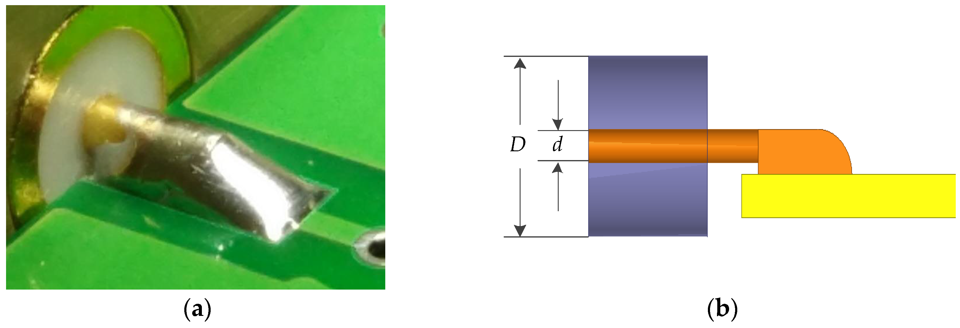
On the other hand, if the inner core of the microwave interconnected structure with the coaxial seal is soldered directly to the substrate, the transition structure will be invalidated due to thermal deformation because of a mismatch in thermal expansion coefficients between different materials and geometric position restrictions. As shown in
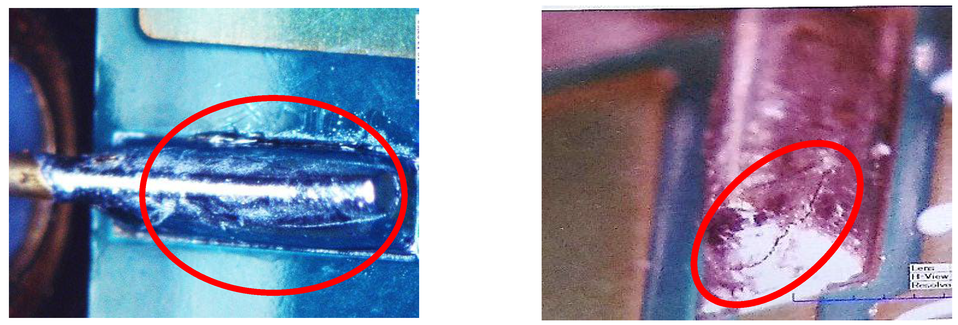
Figure 1, the inner core of coaxial seal and the substrate are directly soldered as a whole and the thermal expansion coefficients between them are significantly different. However, there is no means to release deformation stress in the directly soldered interconnection structure. The temperature change of the package causes a large stress in the solder joint. After multiple temperature cycles, cracks and ultimate failure of the microwave interconnection can occur. The test temperature is −35~70 °C, and the rate of the temperature change is less than 10 °C/min. The limit temperature is maintained for at least 15 min, and a total of 200 cycles are conducted. Eventually, the cracks shown in
Figure 2 will appear. Normally, direct current (DC) characteristics will not be affected, but its microwave and RF signals will be blocked.
Three-dimensional electromagnetic simulation and mechanical analysis of the transition structure were carried out according to the actual design. The microwave transmission characteristics and the solder joint stresses were simulated. The basic structure can be abstracted as two uniform rods fixed together, one of which is fixed at only one end. The stress can be estimated according to the thermal expansion coefficient, elastic modulus, cross-section area, and the temperature change of each material. Because the actual structure is relatively complex, a simulation method was adopted. By establishing the same 3D model as the real structure, and giving mechanical parameters such as thermal expansion coefficient, tensile strength, and Young’s modulus to each part of the structure as
Table 1, the mechanical simulation analysis was carried out after the finite element grid was divided and the connection relationship was set. Taking the seal applied in an aerospace microwave package as an example, the dielectric diameter as D was 1.6 mm, and the inner core diameter as d was 0.3 mm. The materials used for packaging and interconnection structures are as follows:
Various traditional interconnection structures are analyzed in detail, below.
2.1. Directly Soldering Structure
When the inner core of the seal is directly soldered with the substrate, 3D electromagnetic simulation is carried out for its electrical performance to analyze its microwave transmission performance, and the matching results are evaluated with reflection loss (S11). For the reasonable parameters in the structure, the maximum stress at the soldering point reaches 436 MPa, which is far greater than the solder joint stress requirements, and the reliability is poor. Therefore, the solder joint cracking fault as shown in
Figure 2 will occur.
To solve this reliability problem, the coaxial seal and the substrate are usually connected by flexible structures such as wires and strips [
13,
14]. The interconnection modes mainly include core wire winding soldering [
15], gold-ribbon lap bonding [
16] and gold-ribbon wrap bonding [
17].
2.2. Core Wire Winding Soldering
For core wire winding soldering, the core wire is half wound along the axis perpendicular to the transmission direction, and then forms an “Ω” shaped interconnection structure in the transmission direction, as shown in the
Figure 3.
When core wire winding soldering is adopted, the length of inner core is determined by the packaging structure, and the drop between the inner core and the substrate is strictly controlled during assembly with small change. The solder joint stress is about 32 Mpa with high reliability. The corresponding 3D electromagnetic simulation results are as follows, whose reflection loss is already worse than −8 dB at 5 GHz, so the RF working bandwidth is limited to S-band and below.
2.3. Gold-Ribbon Lap Bonding
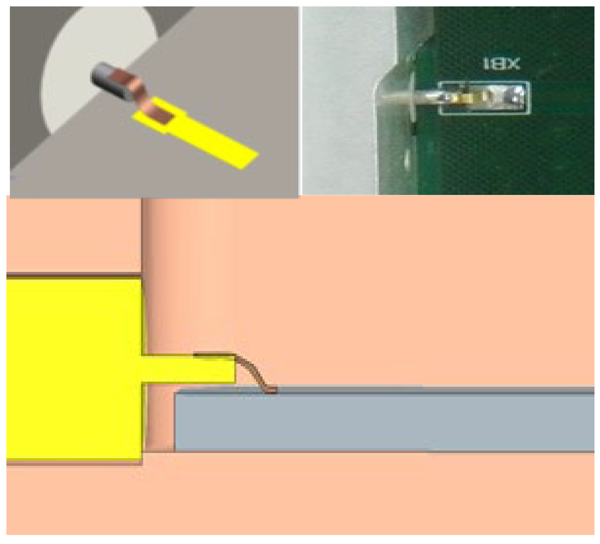
Gold-ribbon lap bonding is the use of a gold ribbon to form a “Z” shape along the transmission line, and the use of parallel gap-bonding equipment to complete the connection of pads at both ends [
16,
18]. The “Z” shaped gold ribbon is usually used for the interconnection of a non-coplanar coaxial seal to plane, such as the connection between the coaxial inner core and the side of substrate, as shown in
Figure 4.
The “Z” shaped gold ribbon is used to connect the inner core of the coaxial structure to the microstrip line of the substrate for gold-ribbon lap bonding. The same method is used to analyze the mechanical stress characteristics. The stress of the ribbon is about 41 Mpa. At the same time, because the length of the ribbon is shorter and the width is closer to the microstrip line, the microwave matching characteristics are better than in the core wire winding soldering. Through 3D electromagnetic simulation, its reflection loss is better than −12 dB below 5 GHz, which can adapt to the transmission of microwave signals in the C-band and below.
2.4. Gold-Ribbon Wrap Bonding
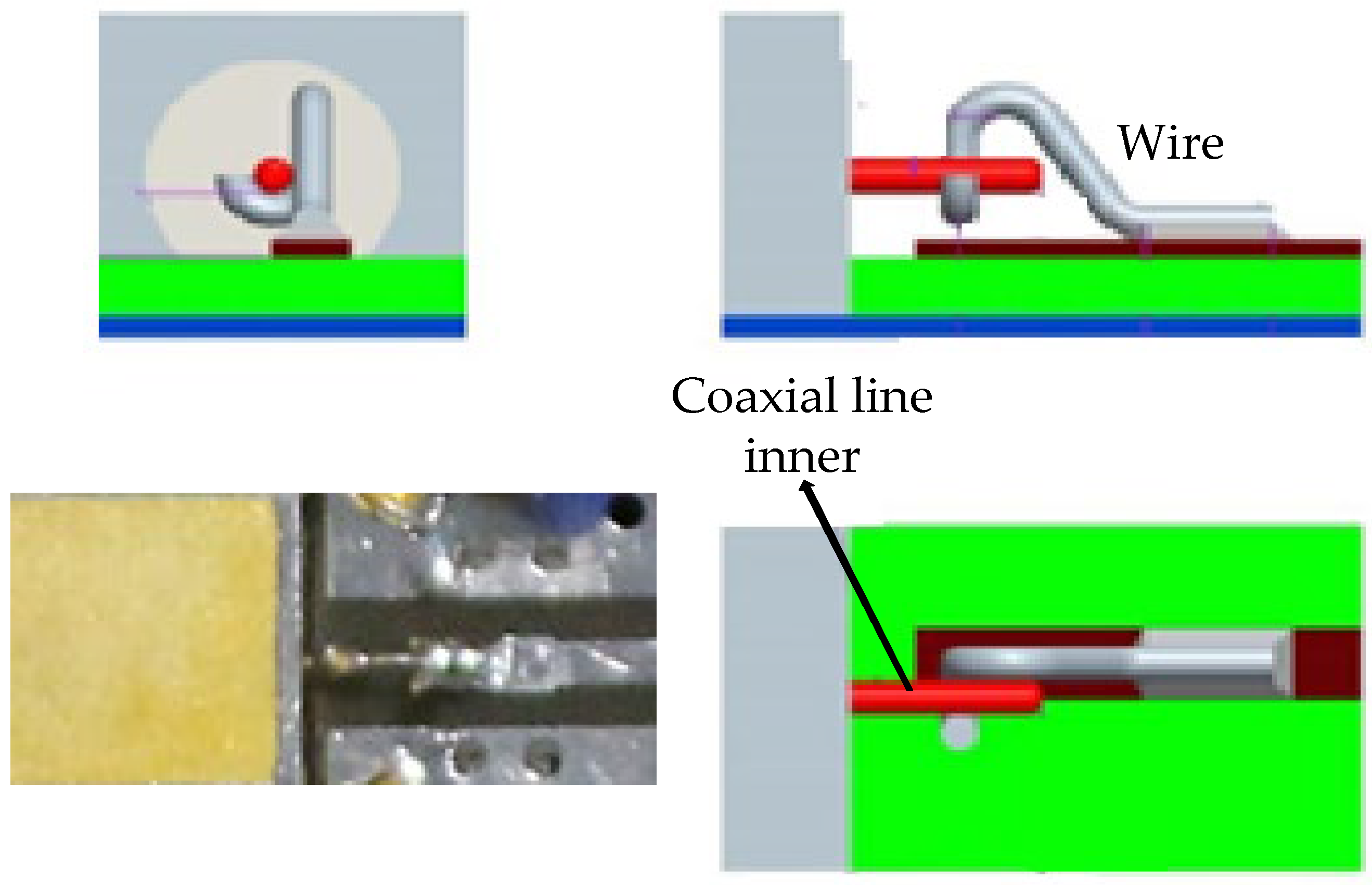
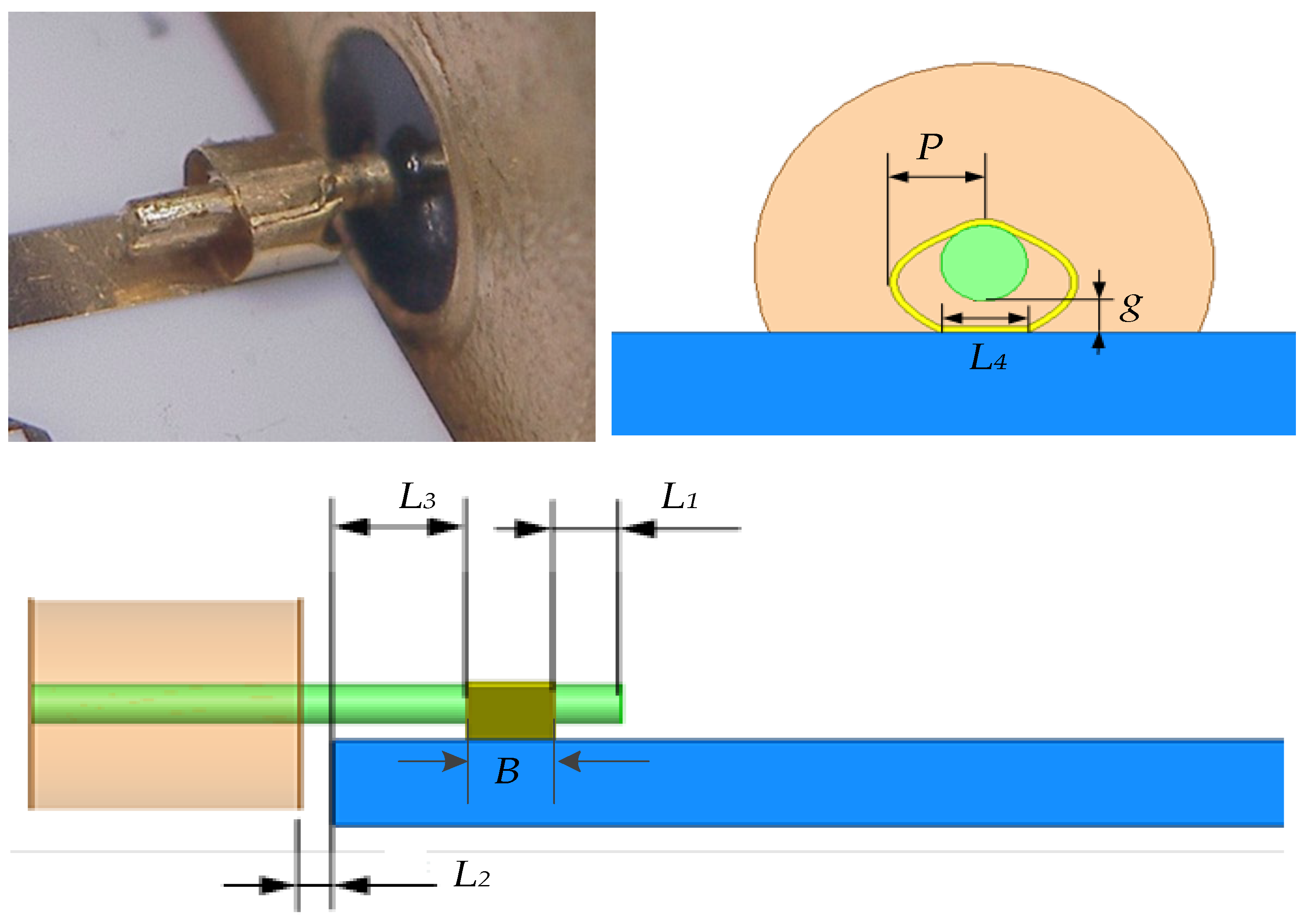
In the gold-ribbon wrap bonding, the ribbon is perpendicular to the direction of transmission line and forms an “O “ shape [
17]. Parallel gap-bonding equipment is used to complete the connection between the strip-line pad and the coaxial lead. The “O” shape is usually used for the interconnection of a non-coplanar coaxial seal to plane, such as the connection between the coaxial structure core and the substrate directly below, as shown in
Figure 5.
After analysis, the distance
L2 from the seal to the substrate and the distance
L1 from the extended end of the inner core to the gold ribbon have little effect on the stress. Therefore, the parameters
L2,
L1, and T are taken as constants, and the parameters
g,
L4,
P,
L3, and
B are taken as variables for analysis. Because there are also ductile connections, the stress characteristics under the same conditions are similar to those of the above structures, as detailed in
Table 2. On the other hand, due to the shorter distance between the abrupt changes of the electromagnetic field mode, the microwave matching characteristics are better than in the lap bonding. Its insert loss and reflection loss are shown in
Figure 6, so this transmission structure can work in the Ka band.
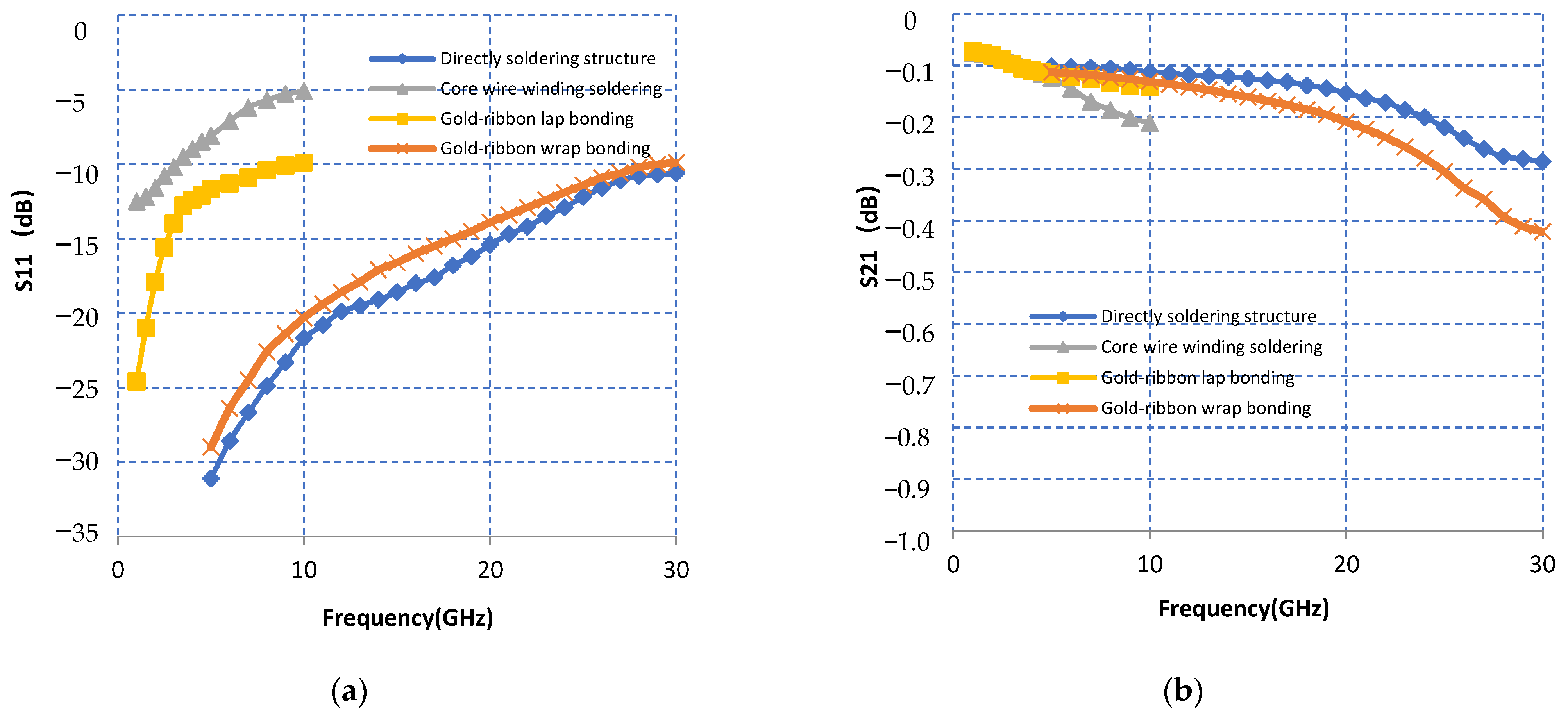
Based on the above, the stress characteristics and electromagnetic matching characteristics of the four structures are summarized and analyzed, as shown in
Table 3 and
Figure 6. Core wire winding soldering, gold-ribbon lap bonding, and gold-ribbon wrap bonding all have better temperature change and mechanical adaptability. The electrical performance of wrap bonding is similar to that of direct soldering. The microwave performance of the wrap bonding can be designed further. Since the gold ribbon in the wrap bonding increases the inductive parasitic parameters, the capacitive matching design is carried out on the microstrip line, as shown in
Figure 7. After matching, its reflection loss can be reduced by about 7 dB, as shown in
Figure 8.
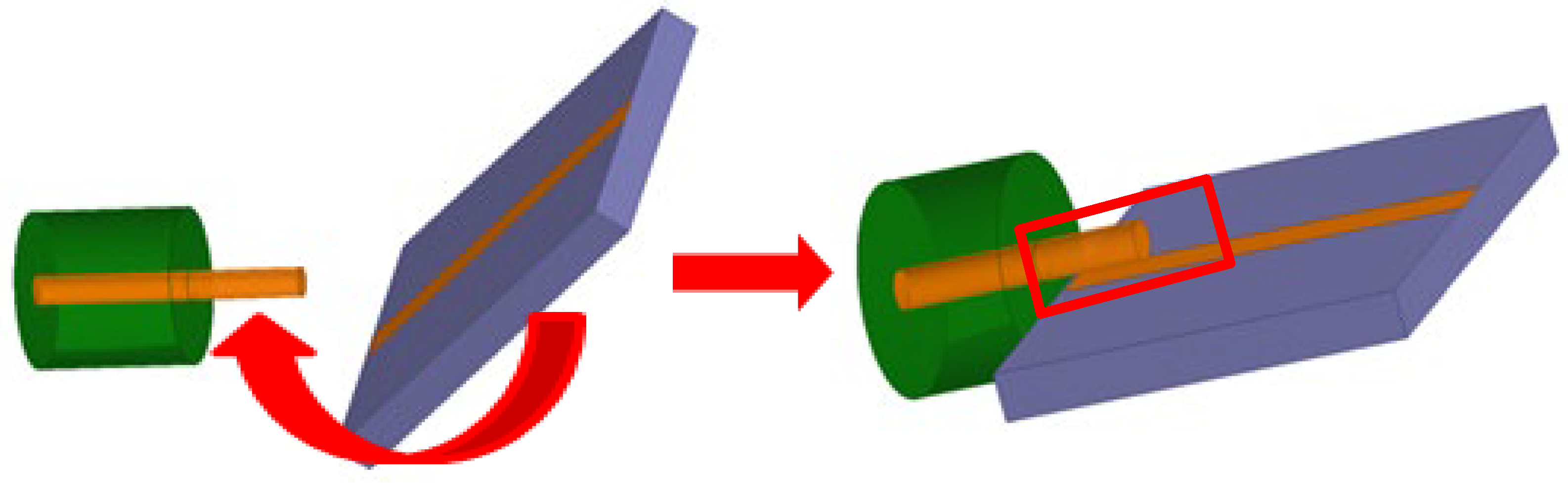
Although the above microwave interconnection structures can solve the stress problem under high reliability requirements, they have poor microwave matching characteristics and it is difficult to apply them in higher frequency ranges. In addition, there is a problem that the inner core of the coaxial seal protruding inward shields the substrate below during assembly. The coaxial seal must be finished after the substrate is assembled, or when the process flow of soldering the shell and seals are first met, and the substrate must be tilted and manually assembled after the coaxial seal is soldered. Therefore, additional processes of microstrip substrate assembly and soldering are created, which greatly hinders the automatic assembly of microwave modules and is not conducive to the mass production of microwave modules, as shown in
Figure 9.
3. A Novel High Reliability Interconnection Structure
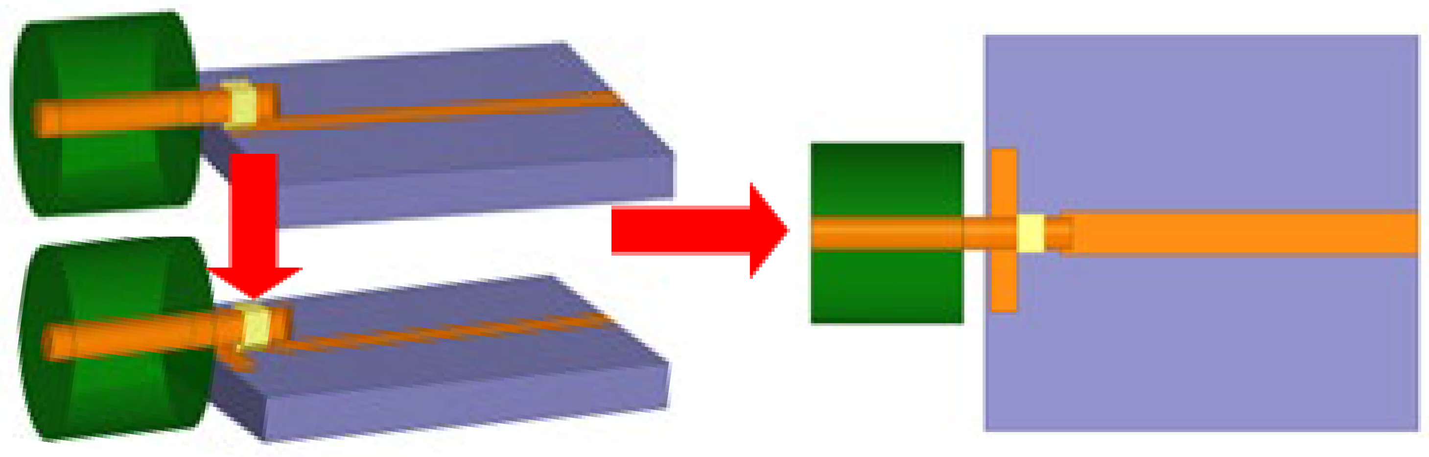
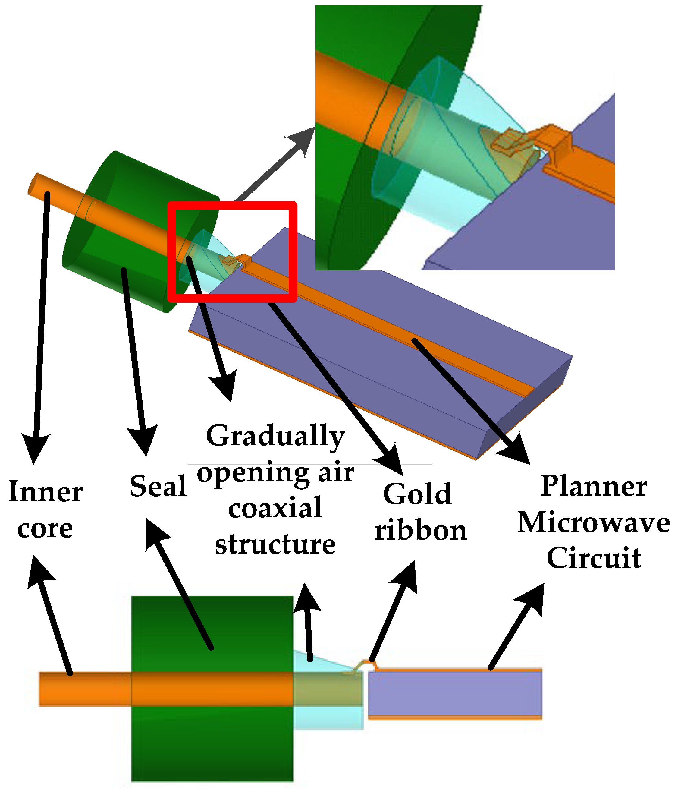
A highly reliable packaging method for space-borne microwave systems is proposed. The metal airtight packaging shell is used, and a new type of horizontal and vertical transition structure is adopted. This structure not only guarantees high reliability, but also achieves good microwave matching in the Ka and above bands, and also avoids the inner core shielding of the microwave dielectric substrate in the vertical direction.
The proposed novel microwave horizontal transmission structure is based on the air coaxial structure with a gradual opening. Specifically, the air coaxial structure with a gradual opening is arranged at the end of the inner core, protruding towards the planar microstrip circuit. The coaxial structure takes the inner core of the seal as the axis, and air as the coaxial dielectric. The air cylinder is cut along the vertex at one end to the center of the circle at the other end to form a gradually opening hollow cylinder. The cutting surface is from the edge of the circular cavity to the diameter of the other end, so as to form a gradual opening on the circular cavity. It makes the complete circular cavity gradually change into the missing semicircular cavity in the upper half, and the missing upper half of the semicircular cavity is an opening structure, which provides an operating space for bonding. One end of the inner core of the seal is exposed to the upper semicircle surface. After bonding, the microstrip circuit is connected to realize the reliable transmission between the inner core and the planar circuit, as shown in
Figure 10.
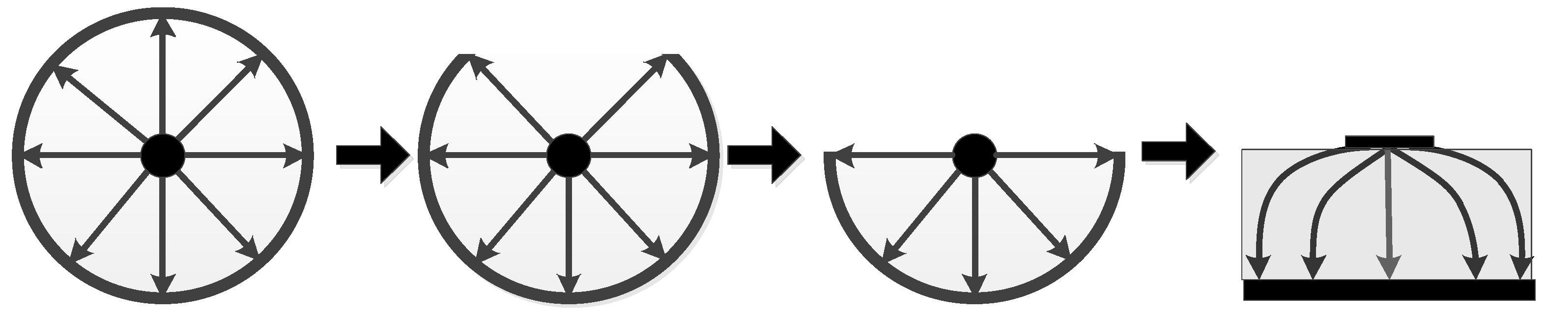
The design uses a gradient approach to transition the coaxial TEM mode to the quasi-TEM mode of the microstrip line (shown in
Figure 11) without a height drop, so that the matching transition from coaxial structure to the microstrip circuit can be achieved in a wide bandwidth [
19]. The method ensures that the inner core of the coaxial seal protruding to the interior does not block the microstrip substrate and can be softly connected together through gold or copper ribbon. The design achieves highly reliable interconnection with excellent electromagnetic transmission performance and an efficient assembly process at the same time.
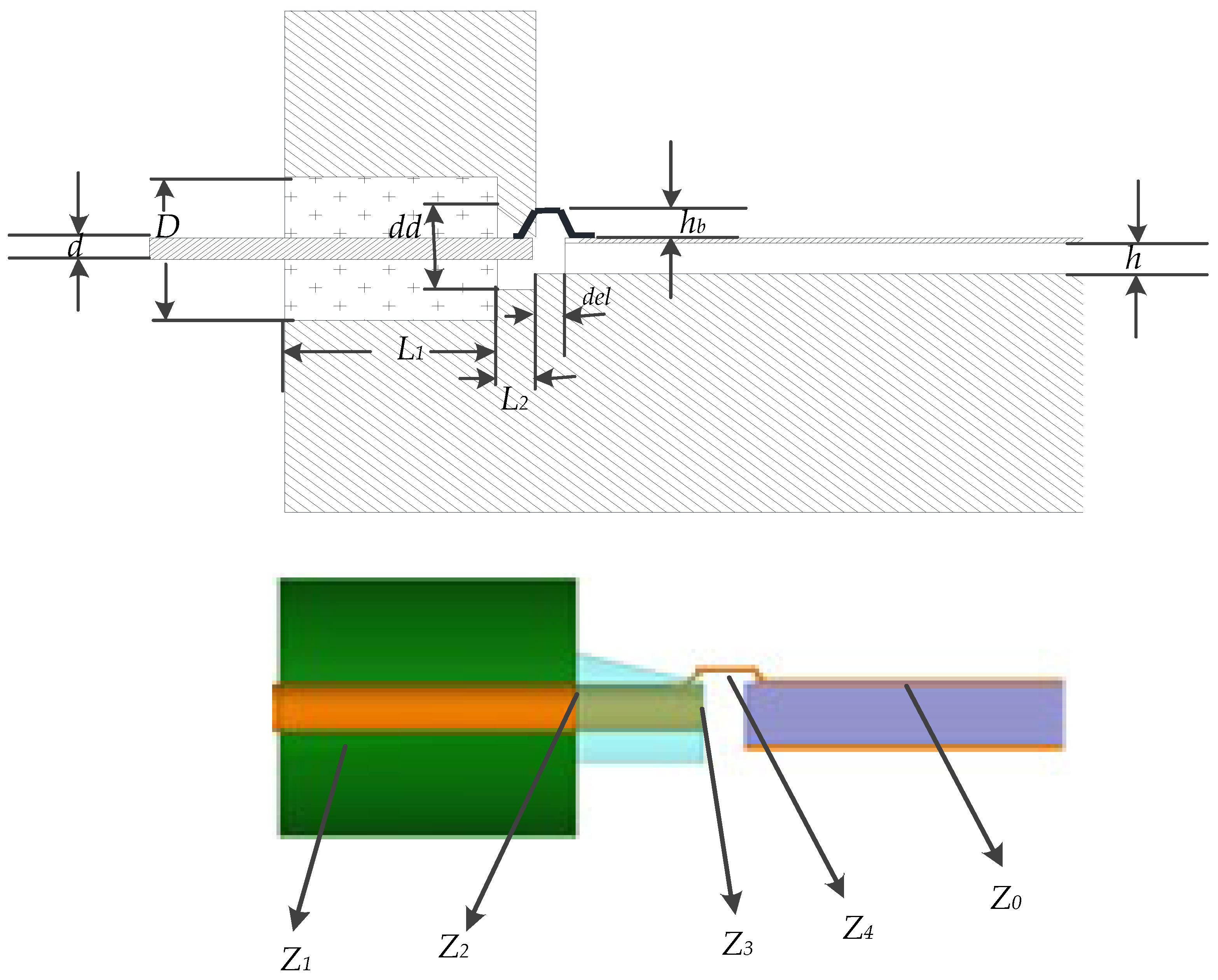
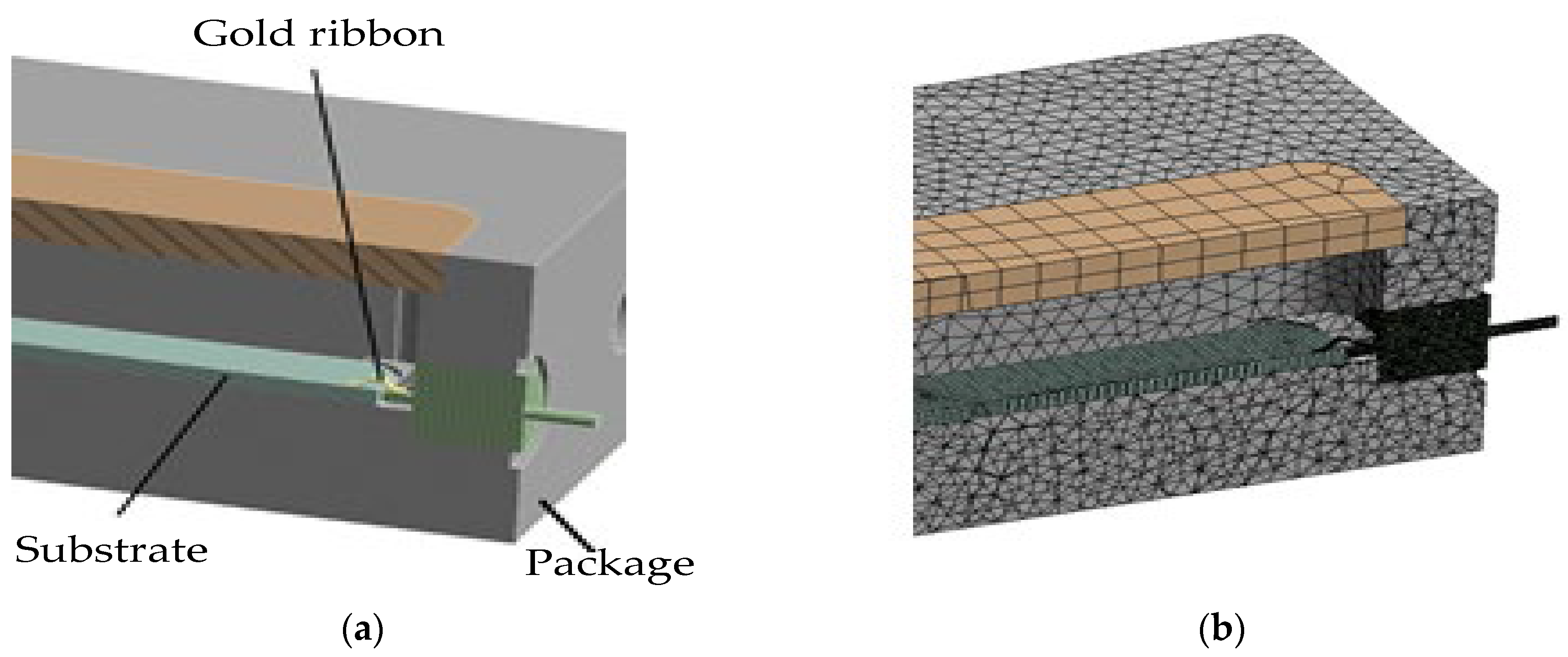
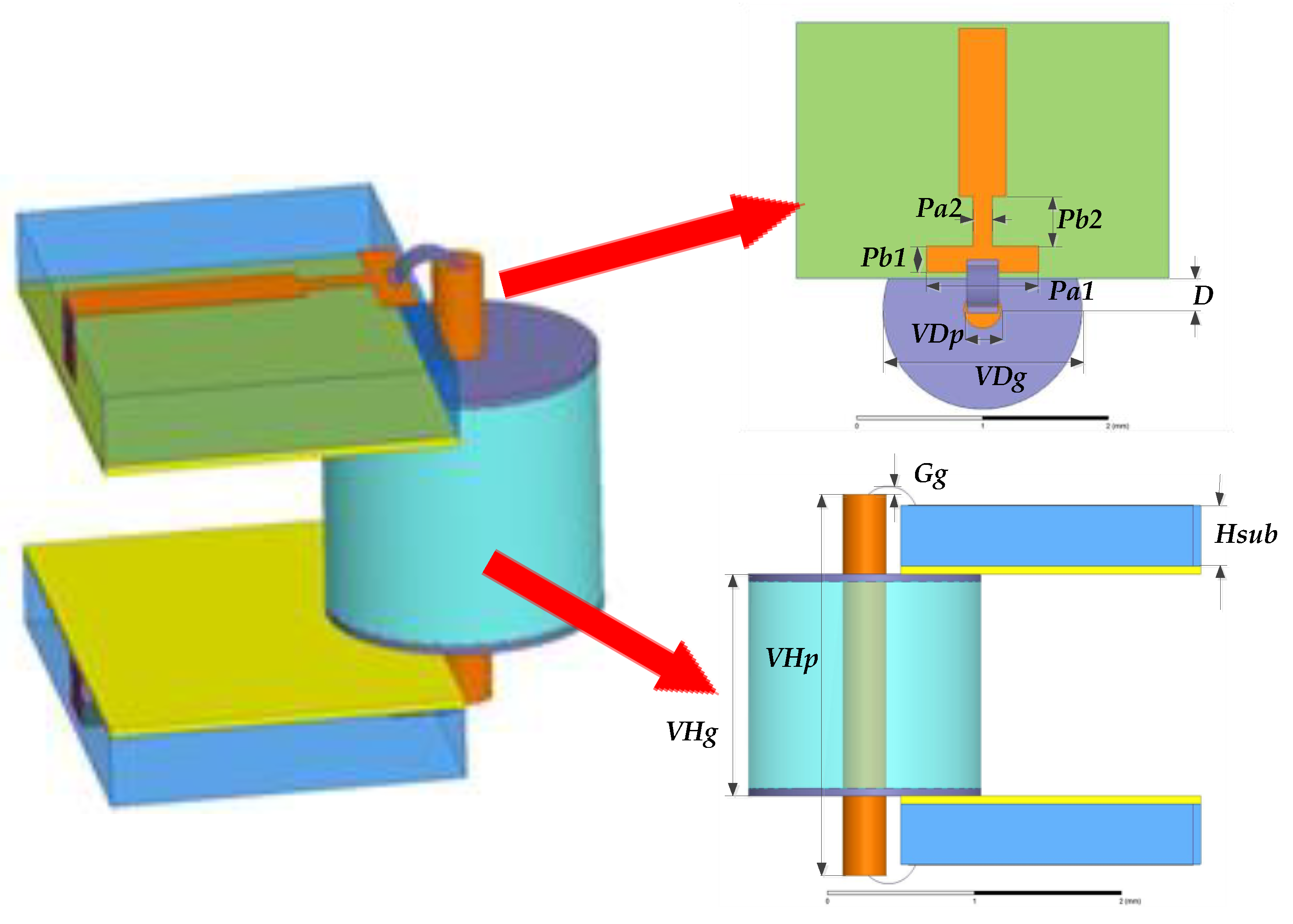
The structure is mainly divided into four parts: coaxial seal, gradually opening air coaxial structure, gold ribbon crossing gap, and planar microstrip line, as shown in
Figure 12.
D is the dielectric diameter of the coaxial seal,
d is the diameter of the inner core of the coaxial seal,
dd is the diameter of the air cylinder,
L1 is the length of the coaxial dielectric,
L2 is the air coaxial length,
del is the gap width between the dielectric substrate and the package wall, the thickness of the microwave dielectric substrate is
h, the width of the microstrip line is
w, the arch height of the gold ribbon is
hb, and the width of the gold ribbon is
Wb. The dielectric constant of the coaxial seal is
εr1, the dielectric constant of the microwave dielectric substrate is ε
r2, and the dielectric constant and magnetic permeability of air are approximate to those of vacuum,
ε0 and
μ0, respectively.
The equivalent transmission line theory [
19,
20] is used to analyze the microwave signal transmission. Impedance matching is required at the connection of each part to ensure good microwave transmission performance. Therefore, the equivalent characteristic impedance of the four parts can be calculated.
The characteristic impedance of coaxial seal
Z1 is:
where
Z0 is the standard 50 ohms. The characteristic impedance
Z2 of the air coaxial end towards the seal is:
From
Z0 =
Z1 =
Z2, it can be seen that:
The other end of the gradually opening air coaxial line is a quasi TEM mode, so it can be equivalent to a curved microstrip line, whose dielectric is air and impedance
Z3, which can be approximated by the microstrip line:
where
We and
he are the width and dielectric thickness of the equivalent microstrip line, and ε
e is the equivalent relative dielectric constant:
The ABCD matrix [
13] can be used to analyze the transmission characteristics of the gradually opening part in the air coaxial structure. It is set to be divided into
n parts. The length of each section is
L2/n, and the characteristic impedance is
Z2i (
i = 1,2,3…
n), where the transmission matrix
Mi can be calculated as:
The total transmission matrix
M is:
As the length of the air coaxial part is usually very short, sin (βL2/n) is approximately equal to βL2/n, where β is the transmission coefficient.
In addition, it can be approximately considered that the equivalent characteristic impedance of the gradually opening part is uniformly transformed from
Z2 to
Z3, i.e.,:
Therefore, the total transmission matrix
M can be approximately expressed as:
The equivalent characteristic impedance
Ze of the gradually opening coaxial structure can be derived from Equation (11).
Moreover, the characteristic impedance
Z4 of the gold ribbon crossing the gap can be approximated as:
where,
hb is the ribbon arch height and
h is the thickness of the dielectric substrate. In order for this structure to achieve excellent matching performance at microwave frequency, it is necessary to:
Therefore,
L2 can be obtained as:
Therefore, the initial values of the diameter
dd and length
L2 of the gradually opening air coaxial line can be calculated based on Equations (2)–(4), (12), (13), and (15), and then the design can be completed by further optimization in the 3D electromagnetic simulation software, such as HFSS. Based on the parameters in the previous example, which are shown in
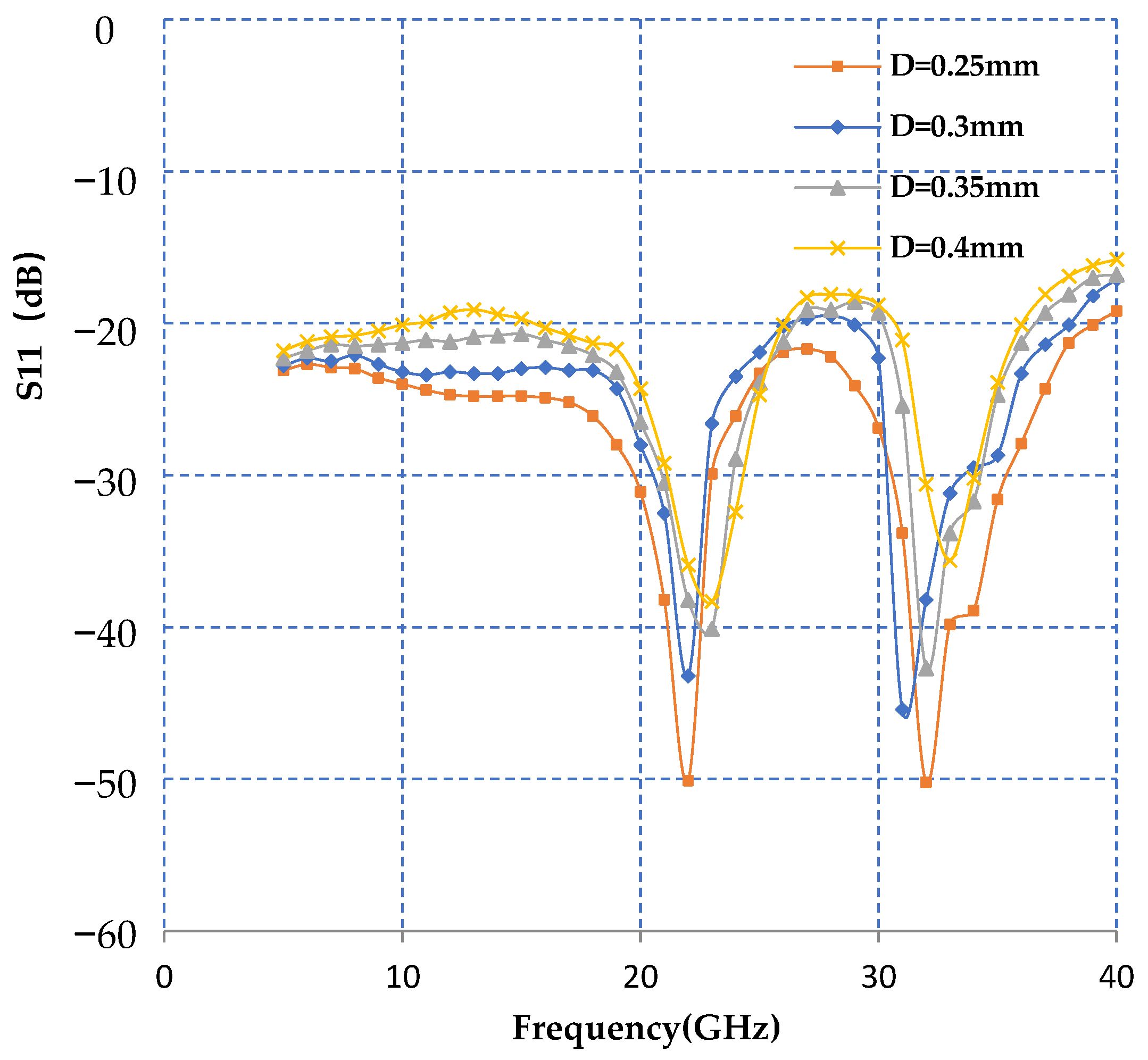
Table 4, the initial values of the diameter and the length of the air coaxial line are calculated to be 0.7 mm and 0.5 mm, respectively.
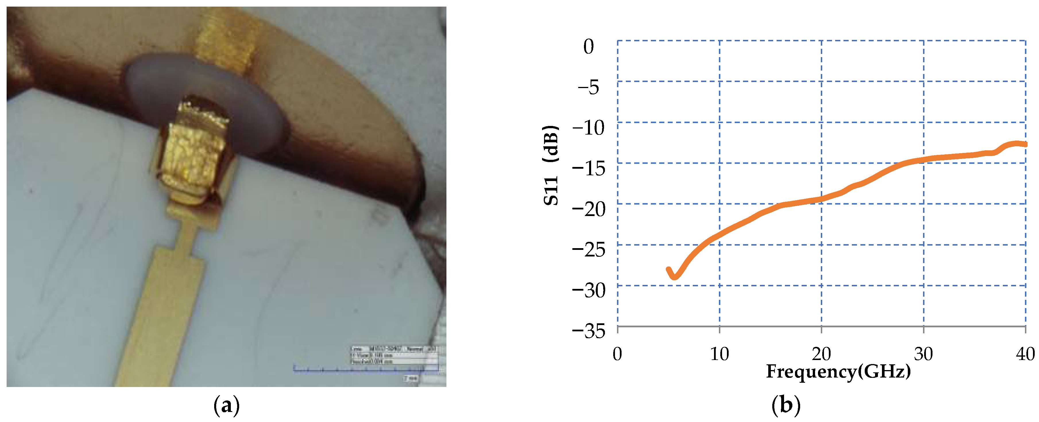
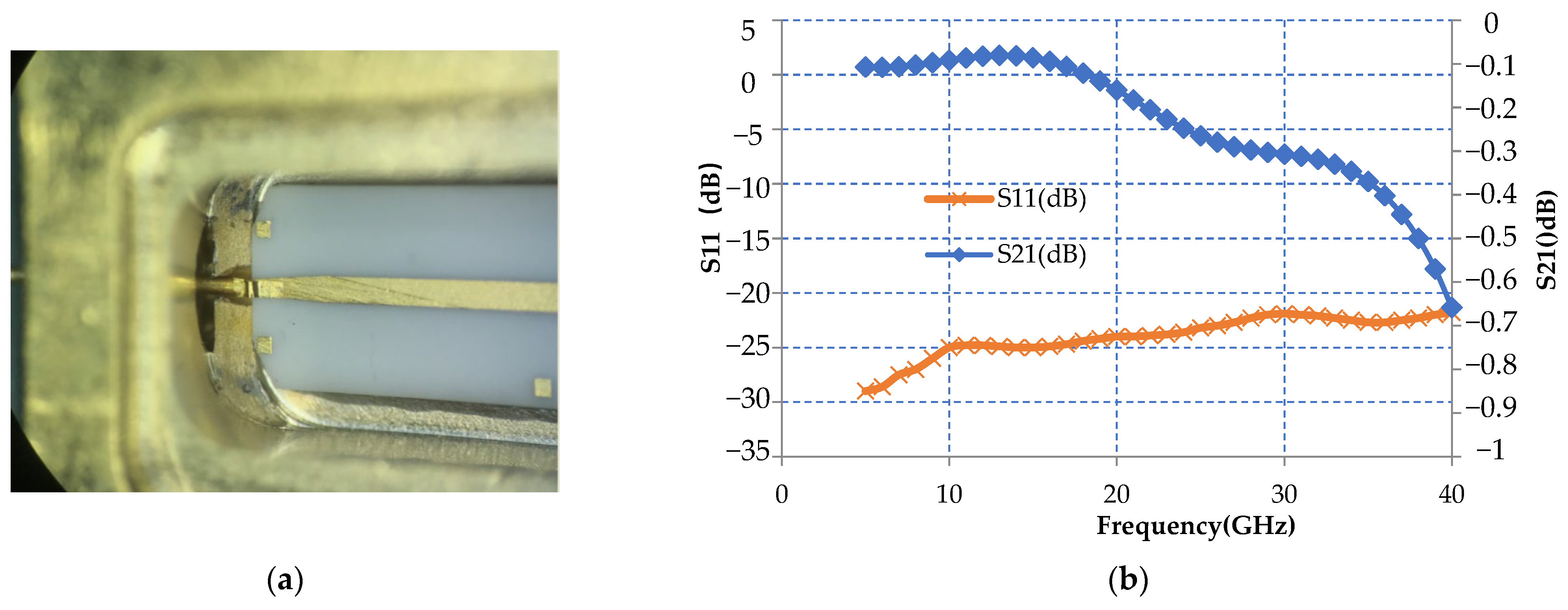
The results of the measured microwave matching performance are shown as
Figure 13.
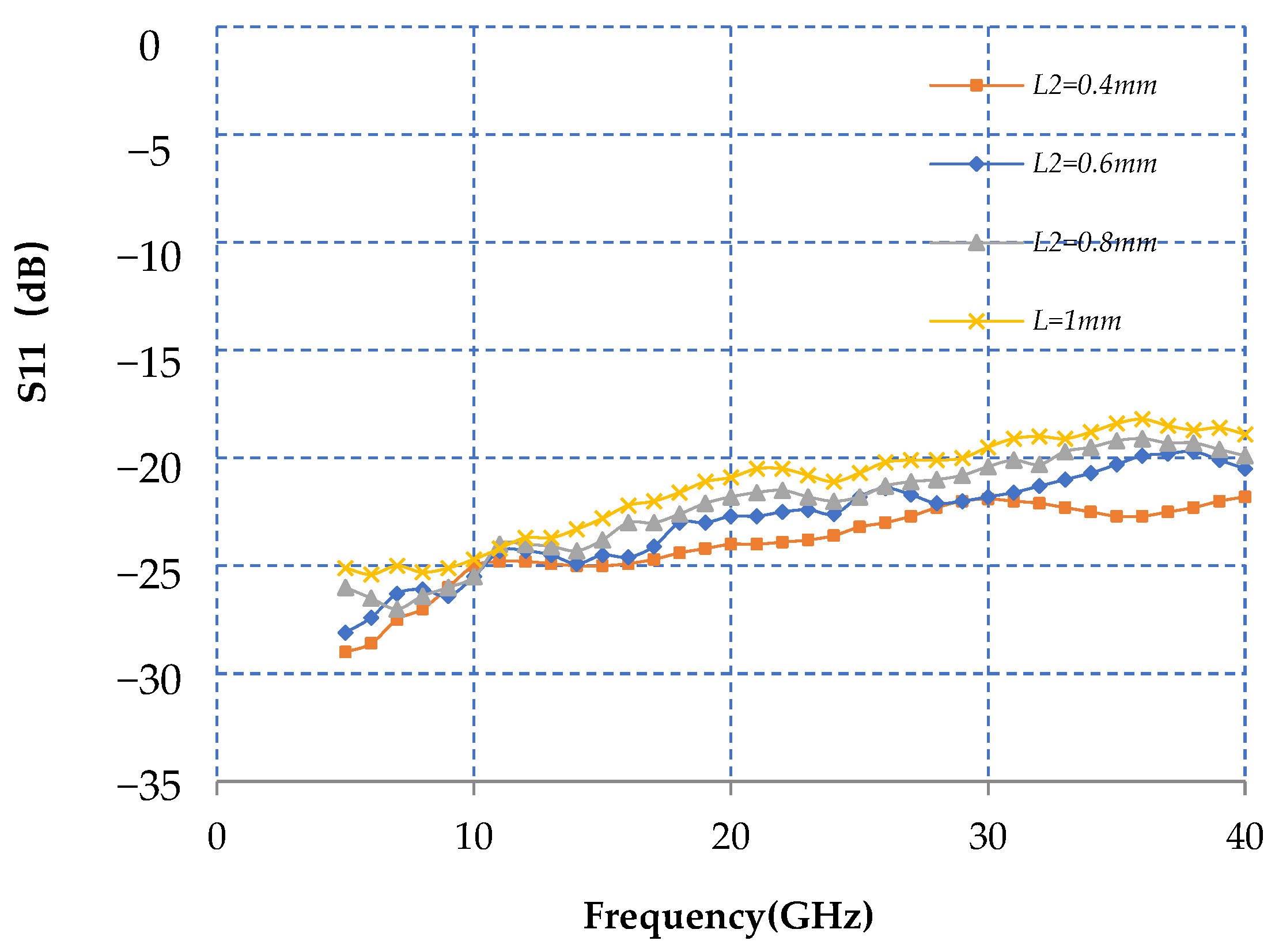
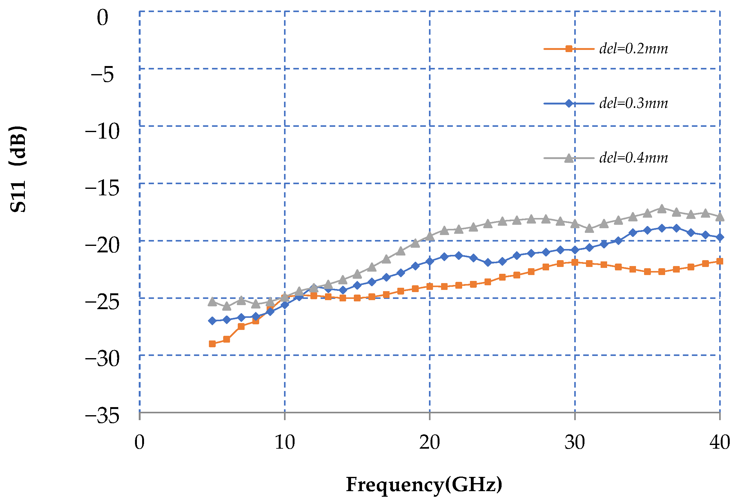
It can be seen that the reflection loss at 40 GHz of the port can be better than −21 dB with this interconnection structure. The length
L2 of the coaxial part in the gradual air can be adjusted during processing, and the gap
del between the inner core of the coaxial seal and the microstrip substrate can be adjusted during assembly. Other parameters are the same as those in
Table 4. Its RF performance is shown in
Figure 14 and
Figure 15. The S21 parameters do not differ much, so detailed analysis is no longer necessary.
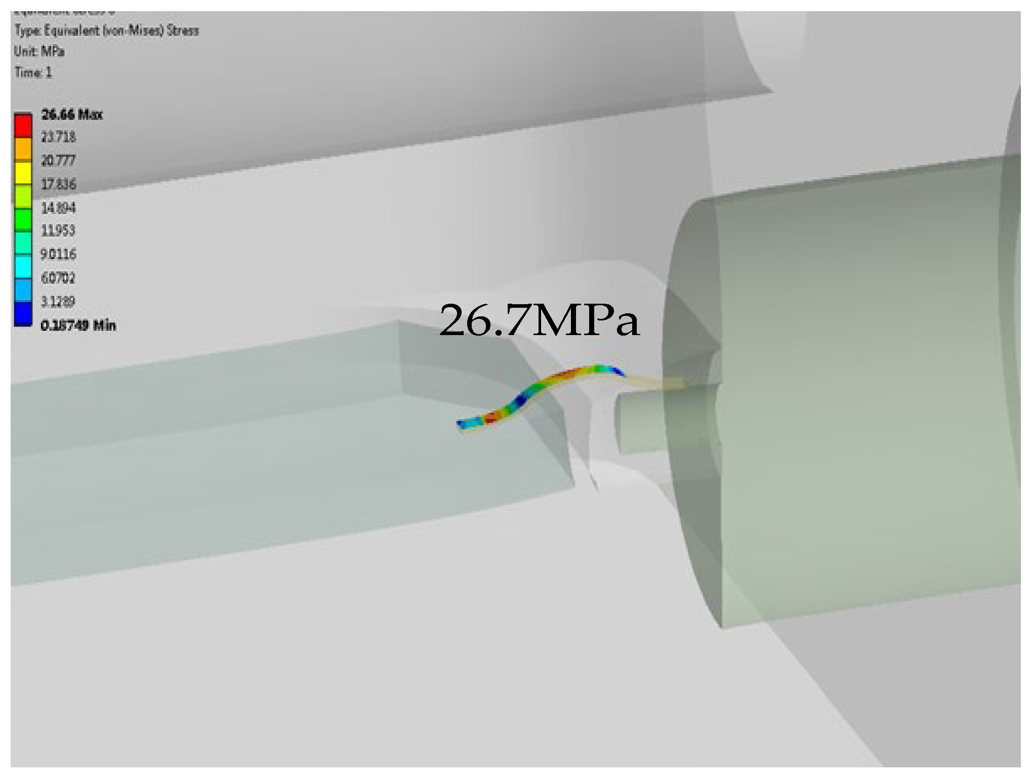
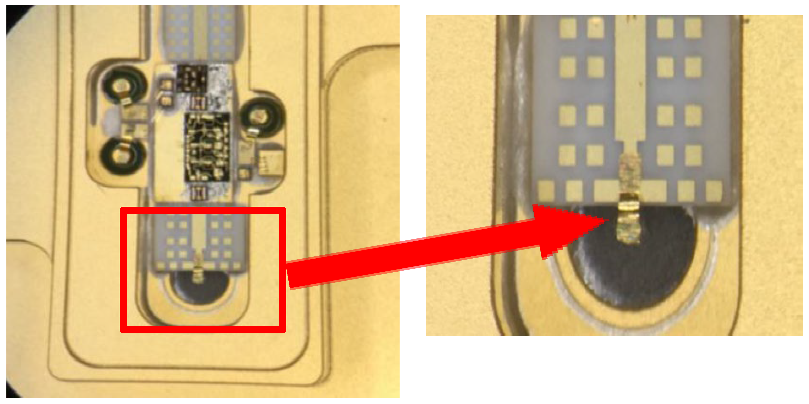
The stress of the structure is also analyzed, and the result is about 26.7 MPa, which fully meets the reliability requirements, as shown in the
Figure 16 and
Figure 17.
The glass seal can also be used to achieve the vertical layout of the microwave circuits [
21], and the bonding gold ribbon can be used to achieve the high reliability of the vertical transmission of microwave signals.
Because the ribbon is used for overlapping and interconnection, the stress is similar to the horizontal interconnection. Only the impedance mismatch caused by the vertical geometric position needs to be solved. High and low characteristic impedance lines can be designed on both top and bottom microstrip lines to match them [
22,
23]. The design is shown in
Figure 18. The main parameters of the vertical transition design are shown in
Table 5.
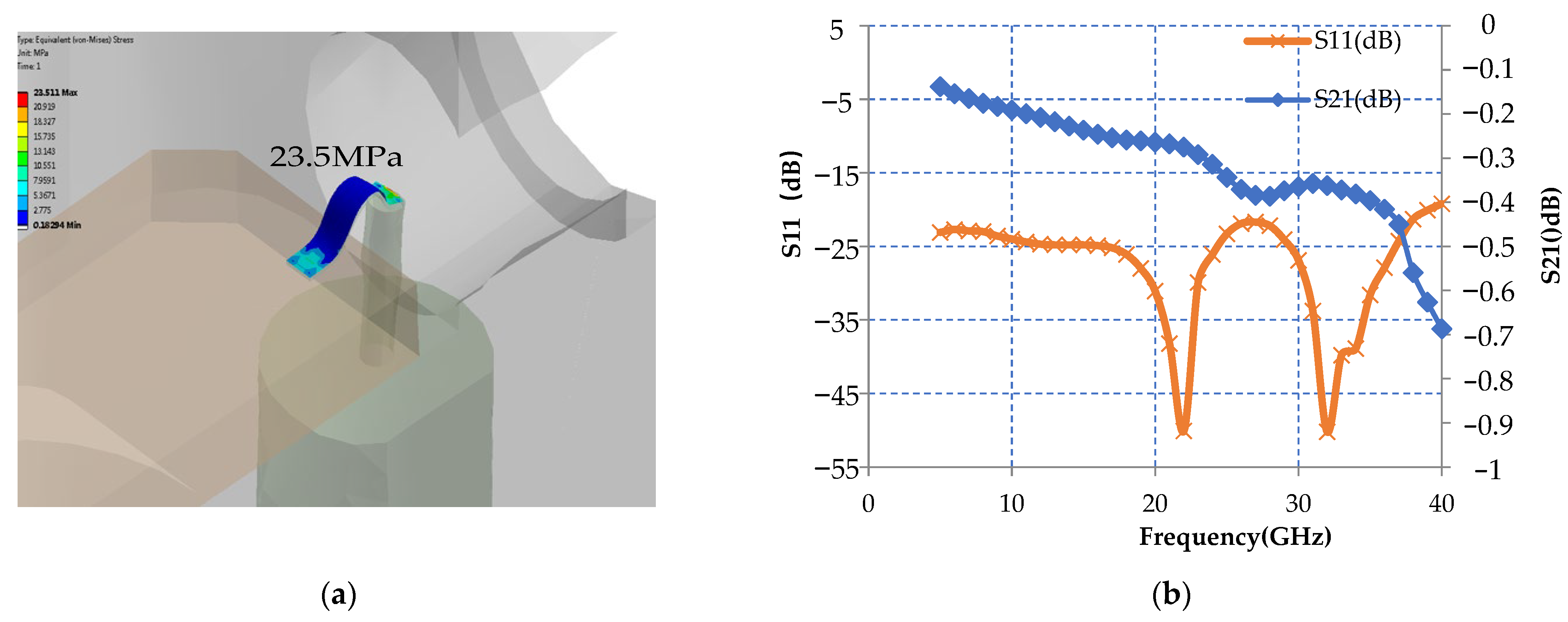
According to the parameters in the above table, the stress analysis and electromagnetic simulation of the vertical transition structure are carried out. The stress is 23.5 Mpa, and the reflection loss is better than −20 dB within 40 GHz as shown in
Figure 19. It has good reliability and microwave transmission characteristics at the same time.
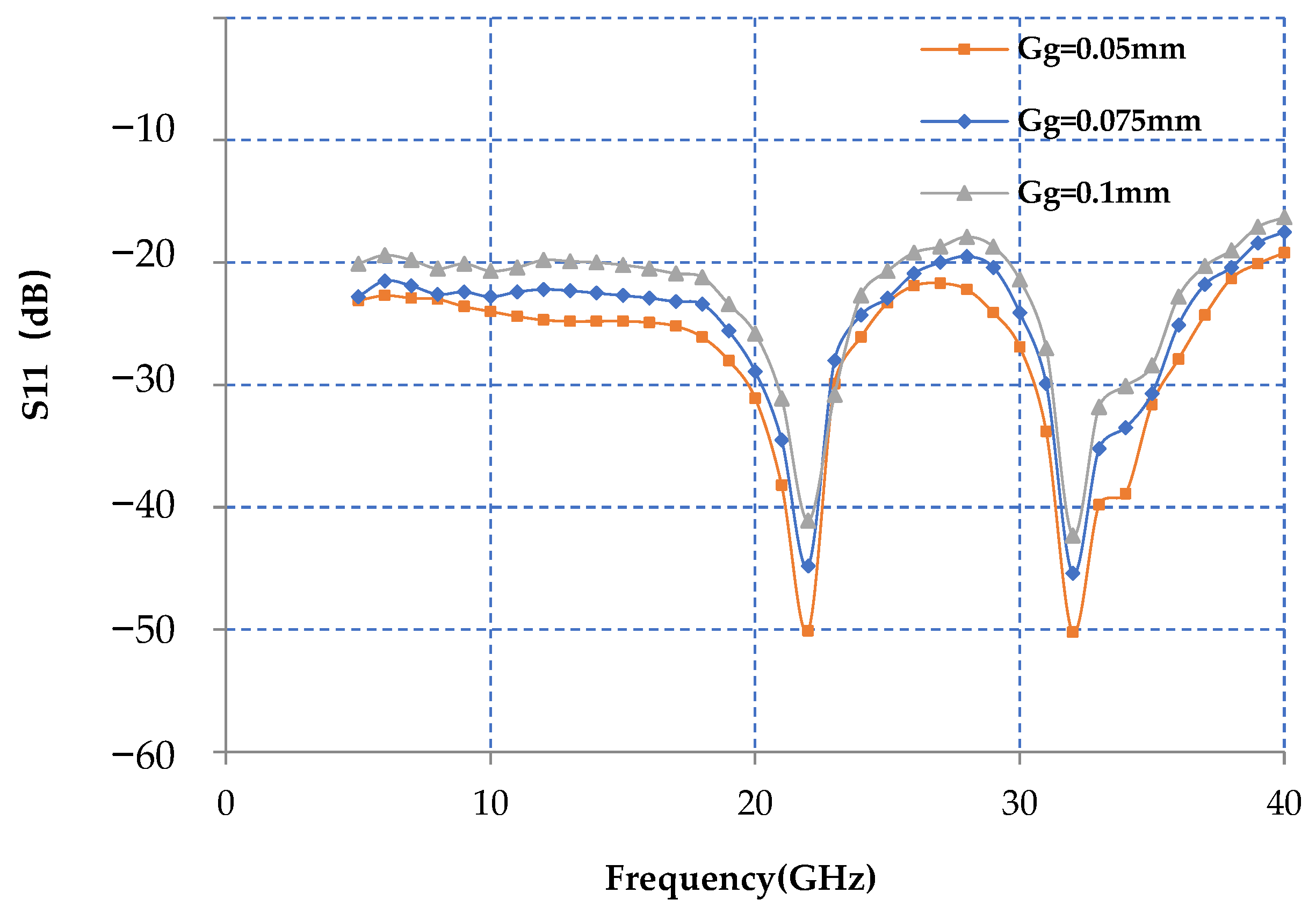
The tolerance analysis of its key dimensions is shown in
Figure 20 and
Figure 21. The arch height of the ribbon and the distance of the gap have little impact on the final reflection loss, which can provide sufficient processing deviation margin for actual assembly.
For the actual process and test, as shown in the
Figure 22, it has achieved excellent RF performance with microwave high-frequency active circuits.
4. Packaging Design and Measurement of a Spaceborne Ka-Band Receiver
The novel high reliability horizontal and vertical transmission structures described above are used for the metallic SIP design of a Ka band receiver. During the Ka band packaging design, the cavity division design is first carried out according to the function, frequency, and gain. Then the transmission structure described above is used to achieve the horizontal and vertical interconnection between the cavities.
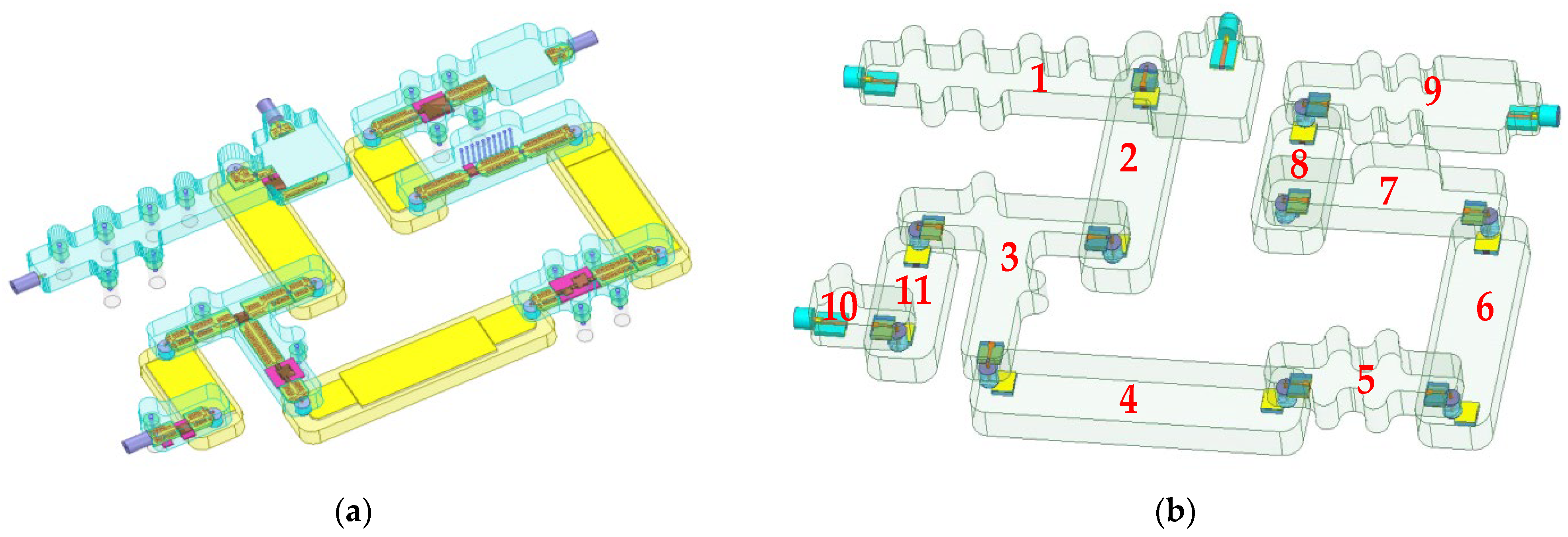
The following aspects need to be considered in packaging design:
Precise cavity division has been made for the Ka band receiver. The top of the packaging structure is divided into seven cavities and the bottom is divided into five cavities. Since the SIP is divided and the horizontal and vertical transition transmission structures are used for interconnection, there will be no space coupling or crosstalk between cavities due to electromagnetic radiation or leakage [
24].
- b.
Resonant frequency design of the cavity.
In order to eliminate the cavity resonance near the working frequency and ensure that the resonant frequency of the cavity is much higher than the working frequency, the dimensions of all cavities are designed and simulated. From the simulation results, all cavities meet the application requirements. The model of the SIP cavities and their lowest resonant frequencies are shown as
Figure 23 and
Table 6.
- c.
Avoid high single cavity gain.
Too high gain in a single cavity will result in self-excitation of the amplifier. Through the cavity splitting processing, the number of amplifiers integrated in a single cavity is reduced. The cavity with the highest gain is the end cavity, and the gain is about 30 dB. Basically, there is no self-excited phenomenon caused by high single cavity gain.
- d.
Enhance space isolation of ports.
In order to prevent the space coupling of RF input and output ports, the ports are placed in different directions in the package. For the local oscillator (LO) input port, in order to avoid insufficient isolation between the output and the LO port, they are also placed in different directions. The spatial isolation is greater than 80 dB, which can well meet the reliability requirements.
- e.
Reduce coupling and crosstalk caused by low-frequency power supply circuits.
In order to eliminate this effect, 100 pf and 10,000 pf die capacitors are connected in parallel at each power supply pad nearby to filter out the stray signals, which come from the low-frequency power supply board. In addition, the power supply pads on the low-frequency power supply board and the vertical power seal are interconnected nearby, and the uF-level capacitor is connected in parallel nearby for filtering, so as to eliminate the crosstalk between low-frequency and RF to the greatest extent.
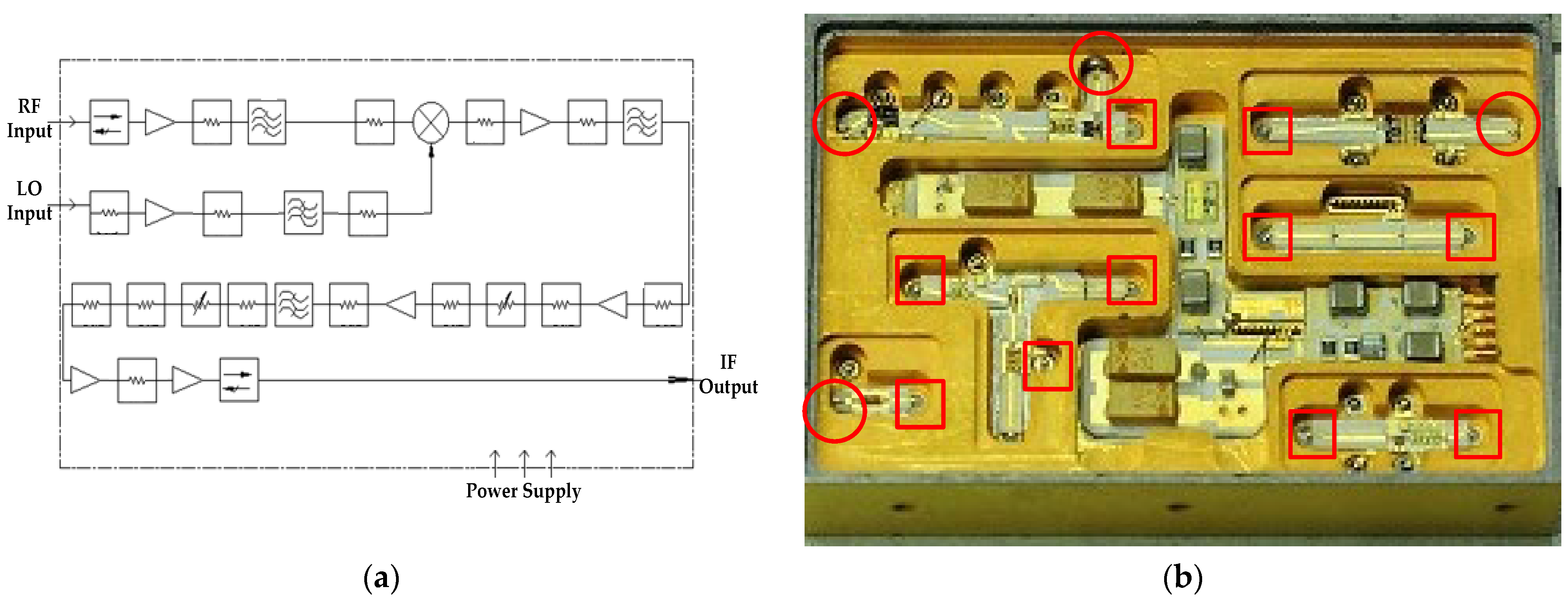
Based on the method above, this spaceborne Ka band receiving SIP is composed of an RF low noise amplifier, an RF amplifier, an image rejection filter, a mixer, an intermediate frequency (IF) band-pass filter, an IF low power amplifier, an IF medium power amplifier, and an attenuator. It was manufactured, and the diagram and the photo are shown in the
Figure 24. The circles show the locations of the proposed horizontal interconnects and the rectangles show the vertical ones.
The design completes the functions of low noise amplification, frequency conversion, gain amplification, gain adjustment, and harmonic clutter filtering. The RF circuits are cascaded by microwave dies, microstrip lines on the substrate, and other devices by the novel interconnections above. The top and bottom circuits are interconnected through the novel horizontal and vertical seals. The local oscillator chain completes the functions of frequency doubling, gain amplification, and filtering. The local oscillator chain is similar to the RF, and it is realized by cascading dies and microstrip lines with the same interconnections. After the measurement, the SIP was subjected to a temperature cycling test of −35~ +70 °C for 200 cycles, followed by a mechanical impact test with a peak acceleration of 1500 g and a pulse width of 0.5 ms. After the environmental compatibility tests, the system package was tested again, and its performance was still excellent, as shown in
Table 7.
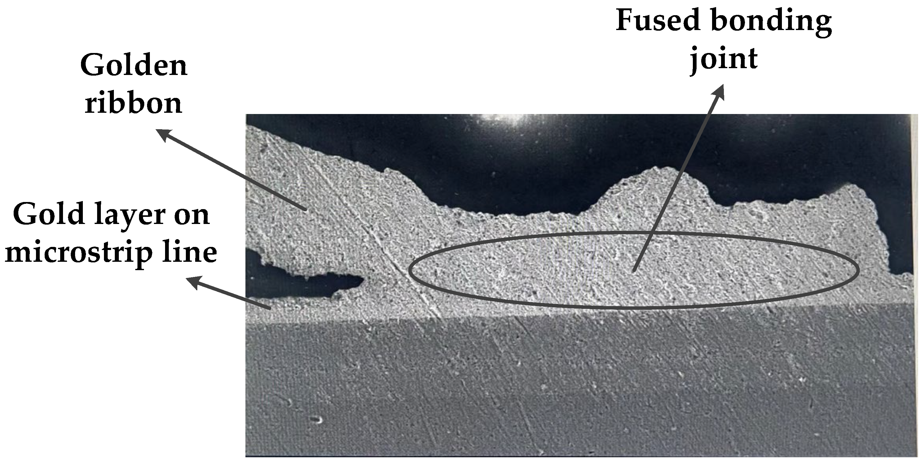
After the new interconnection structure is applied to the metal 3D-SiP for aerospace, the improvement and optimization characteristics of the interconnection structure can only be evaluated through the performance of the entire SIP, especially the amplitude flatness and noise figure indicators. If the new transition structure is replaced by a gold-ribbon lap bonding structure, its amplitude flatness will deteriorate to 1.3 dB, and the noise coefficient will be 2.9 dB. Therefore, it can be seen that SiP based on the new transition structure has good matching characteristics. On the other hand, according to the metallographic analysis of the solder joints in the new SiP after the temperature cycling test, the contact is still good, as shown in the
Figure 25.


