Abstract
This paper presents a low-loss, high-transmission, broadside-coupled, transverse, reciprocal, two-port, and nature-inspired Ka-band transition design to move the electromagnetic energy of a rectangular waveguide (RWG) to the microstrip (MS) line. The proposed transition is simple in structure, with an excellent insertion loss, S12/S21, (IL) near −0.40 dB and return loss, S11/S22, of <−21 dB, while the VSWR value is very close to one. Thus, this transition is an outstanding candidate for MIC/MMIC-based millimeter wave, military, and RADAR applications, as well as in wireless and satellite communications as a compatible connector. This transition also provides a bandwidth of 21.50 GHz (23.52–45.0 GHz) for the abovementioned microwave applications, at a <−10 dB return loss (RL). The proposed transition model also exhibits a −15 dB absolute bandwidth of 27.06–23.44 GHz, with an insertion loss < −0.60 dB. Due to a return loss of <−15 dB over an ultra-wide bandwidth, the proposed transition is not only a good candidate for full Ka-band (26–40 GHz) applications but also covers applications for K-band from 23.74 GHz to 26.0 GHz, Q-band applications from 33.0 to 45.0 GHz, and U-band applications from 40.0 GHz to 45 GHz, with approximately 97% power transmission between the transmission lines and only 3% power reflections. The impedance matching at the designed frequency between the RWG and MS line is achieved by flaring one end of the MS line inside the RWG in a fishtail shape, without the need for a quarter-wave/tapered/exponential/Binomial, or multi-section Chebyshev transformer. The main goal of this research was to design a multi-section impedance-transformer-free, simple, and easy-to-fabricate MS line, to share electromagnetic (EM) energy between an MS line and RWG in 30 GHz satellite applications and 30 GHz high-frequency applications, for interconnects screen printed on an organic substrate for flexible, wearable, textile conformal antennas. This work also presents an exact RLC electrical equivalence model of the MS line (fishtail) to RWG transition at 30 GHz. The novelty of this work is that the proposed transition can be used for four microwave bands of electromagnetic energy transmission, with extremely low reflection, and with a compact, simple-design MS line, and simple RWG.
1. Introduction
With the increasing demand for planar circuits (MMIC and MICs) to couple electromagnetic (EM) energy with waveguides and vice versa in the field of millimeter wave, wireless, satellite, and RADAR communication applications, the construction of a compact, multi-section impedance-transformer-free, simple, and precise structure is highly desirable. Current technological development is such that MIMO transmitter and receiver systems, integrated multiple-input multiple-output (MIMO) antenna solutions for long term evolution (LTE) and millimeter-wave (mm-wave) 5G wireless communication services, Wi-MAX, 5G and 6G technologies, RADAR (phased array radar, tracking, and speed measurement RADAR), and wireless communications (front end receiver, transmitters and receivers components, varactor modulators) require a connector or transition that can connect with them and that can couple EM energy through their respective transmitter/receiver antenna systems and then transfer this energy into planar (MMIC or MIC) circuits for further processes, as well as in the reverse direction. The two most promising approaches to these transitions for satellite communication and military applications are mode transformation from the quasi-TEM mode of the microstrip line (MSI) to the rectangular waveguide (RWG) dominant mode (TE10), and impedance or filed matching among the two transmission lines [1,2]. Therefore, for the fulfillment of these requirements, many such waveguide-to-microstrip line transitions have been designed and developed based on the use of different coupling methods and techniques [1]. To continue this development, this paper presents a Ka-band rectangular microstrip-to-waveguide (MS-to-WG) transition for sharing power transfer, using a fishtail-shaped microstrip launcher.
2. Literature Survey
A rectangular waveguide (RWG)-to-microstrip line (MSL) transition is a two-port hybrid connector. It can transfer electromagnetic (EM) energy from a microstrip port to a waveguide port with minimum attenuation and low transmission losses. For wireless applications, RADAR applications, and millimeter wave applications, the designed transition requires a wide bandwidth across the determined center frequency. To meet these requirements, an enormous amount of research has been carried out and will be continued [1]. Jin Li et al. proposed a narrow wall side inserted Ka-band semicircular ring magnetic coupling based RWG-to-MSL transition. It is compact and easy to manufacture. It also possesses a wide bandwidth for the full Ka-band. Nevertheless, it has poor insertion loss lies between −1 dB and −2 dB [3]. Shih et al. designed a Ka-band 90° E-plane transition consisting of a multi-section step impedance transformer with minimum reflection and transmission losses over a fractional bandwidth (FBW) of 40% [4]. S. Tomar et al. presented an E-probe Ka-band Ms line-to-RWG transverse transition. This transition uses a single-step impedance transformer with an IL of −0.30 dB over 14.54% FBW [5]. Varshney et al. proposed an E-plane transverse transition using a two-step impedance transformer and a rectangular probe, with low reflections below a −10 dB bandwidth of 38% [6]. In this Ka-band E-plane side inserted RWG-to-MSL transition, impedance and field matching is possible by employing a multi-section microstrip line transformer [1,3,4,5,6]. This results in good insertion loss (IL), S12 and return loss (RL), and S11 with a bandwidth below −10 dB; in addition, it has a high degree of integration with MIC and MMIC circuits and devices. Yu Lou et al. presented an E-plane 90° inline MSL-to-RWG transition. Their design comprises a radial-shaped probe with a notch cut in the main microstrip, and an extended ground to match the field and impedance of the dominant waveguide mode. This transition exhibits a wide bandwidth, with satisfactory insertion and returns loss for the entire Ka-band [7,8]. Tang C. et al. demonstrated and fabricated an E-plane 90° inline transition using a semicircular loop with a broadband bandwidth lower than −20 dB return loss for the full Ka-band, using a single-step impedance transformer. The design also utilizes a thin-film resistor as a termination load [9]. C. Long et al. demonstrated an inline, low-cost, single-sided PCB, and impedance-transformer-less MS-to-WG transition with an IL of −0.40 dB for a wide fractional bandwidth of 71.43% [10]. R. Gupta and P.P. Kumar proposed a transverse waveguide to coaxial transition, and field matching and impedance matching were achieved with a ridged waveguide, customized coaxial probe, and back-short distance. This transition had an IL of −0.47 dB [11]. Simone et al. investigated an inline Q-band transition, using a section of a ridged waveguide and Chebyshev impedance transformer, with an IL of −0.26 dB over an FBW of 40% for the entire Q-band [12]. These conductive traces printed on flexible substrates offer many potential applications in the area of wearable electronics, ranging from search and rescue operations, to health and physiological monitoring. Lim Y. Y. et al. investigated the effect of the pasting property on the dc conductivity of printed interconnects on a substrate, as well as the consequent RF performance up to the frequency of 30 GHz [13].
It is concluded from the background literature on MS line-to-WG transitions that, in most of the transitions, the microstrip line must contain a multiple section/single step Chebyshev impedance transformer or ridge waveguide structures. Therefore, the main objective of this article was to design the simplest, via-less, multi-section impedance transformer-less, microstrip line to rectangular waveguide transition for Ka-band operations and interconnects for high-frequency flexible organic substrate screen printing. Another objective of this work was to design and develop an E-plane probe transverse transition with high transmission (i.e., low IL) and low reflections (i.e., RL < −10 dB) over a wide fractional bandwidth (FBW). This paper presents the design and development of an E-plane, broadside inserted 90° K-/Ka-/Q-/U-band RWG-to-MSL transition. The proposed transition eliminates the need for complex multi-section microstrip transformers for impedance matching. This makes the design simpler than the existing one, as field matching and impedance matching, i.e., low reflections, are achieved just by varying the fishtail structure probe width and depth (a novel technique for impedance matching), slot height, and back-short distance. These parameter variation effects are discussed throughout the paper. The proposed transition also shows a wide bandwidth for a return loss lower than −10 dB.
3. Materials and Methods
3.1. Transition Design Equations and Parameters
A two-port rectangular waveguide WR-28 with a broadside dimension (a) of 7.112 mm and width (b) of 3.556 mm to microstrip line transition was designed for full Ka-band operation, using ANSYS HFSS software. The waveguide length of the design was chosen as an integer multiple of λg/2. The basic analytical calculations were made using standard mathematical relationships and the principle of an air-filled 500 Ω WR-28 (RWG) and 50 Ω microstrip line [1,3,4,5,6]. A window or slot was cut at a distance λg/4 from the shorting (back short) end of the RWG. The slot height and width were optimized using thumb rules for better transmission between the MSL and RWG, as depicted in Figure 1a,b. A 50 Ω microstrip was fabricated on double-layered RT Duroid 5880 substrates using photolithography and etching. The optimized dimensions of the 3D-transition model are shown in Table 1 and illustrated in Figure 1a,b. The substrate used at 30 GHz was a soft substrate Roger RT 5880 (Duroid) with a loss tangent of 0.0009. The microstrip line comprised a partial ground plane that just touched the slot/window placed at a back-short distance (d = λg/4) from the guided wavelength of the WR-28 at the bottom surface, and a patch with a fishtail-shaped probe was printed on the top surface of the substrate, as shown in Figure 2a–c. At a Ka-band frequency of 30 GHz, the following design equations were used for the microstrip line and waveguide analysis [14,15,16]:
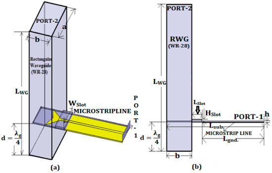
Figure 1.
(a) Rectangular−waveguide to fishtail-shaped microstrip line transition at 30 GHz. (b) Side view of the rectangular waveguide to fish-tail-shaped microstrip line transition at 30 GHz.

Table 1.
Dimensions of the Ka-band MS Line-to-RWG Transition.
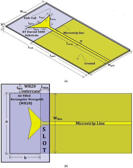
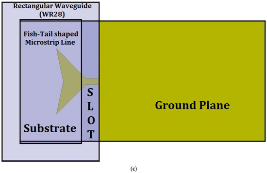
Figure 2.
(a) Fish-tail-shaped microstrip line. (b) Fish-tail-shaped microstrip line top view strip conductor. (c) Fish-tail-shaped microstrip line bottom view ground.
3.1.1. Microstrip Line Calculations
The following design Equations (1)–(5) were used for the design calculations of the microstrip line [14];
The effective dielectric constant;
where = dielectric constant of the substrate,
- w = width of the microstrip,
- h = height of the substrate
where, = designed frequency
where,
3.1.2. Rectangular Waveguide Calculations
The following design Equations (6)–(11) were used for the analysis of the rectangular waveguide [15]:
where, m = 1 and n = 0 for the TE10 mode,
Dominant modes; TEmn = TE10
- a = breadth (broadside) of the waveguide,
- b = width of the waveguide
where,
where, N = any integer value other than zero.
3.1.3. Microstrip Patch Calculations
Since the microstrip probe is used for energy launching in a rectangular waveguide, it behaves like an antenna/energy launcher. Therefore, the following microstrip rectangular patch antenna design (Equations (12)–(16)) was used for the analysis of the microstrip probe/patch [16]:
where, ; where,
Patch Length; LP = L − 2·∆L
N = any integer (1, 2, 3……)
3.2. Field and Impedance Matching
The field matching of the rectangular waveguide dominant TE10 mode with the quasi TEM mode of microstrip line was achieved by varying the slot height, width, and back-short distance of the microstrip from the waveguide. The back-short distance was kept close to the quarter-guided wavelength at the design frequency to reduce reflections from the waveguide back-short end. This field-matching process is known as mechanical tuning. The impedance of the microstrip was 50 Ω, and that of the WR-28 was about 500 Ω. This significant difference in impedance was matched by varying the shape, size, and width of the conductor strip probe inserted inside the waveguide through the waveguide slot, as well as through variation of the substrate width. Ultimately, a tapered fish-tail-shaped probe gave a better impedance matching for maximum EM energy transformation by varying the depth and width. This impedance-matching process is called electronic tuning.
3.3. Optimization of the Back-Short Distance
Ideally, a window/slot is cut into the broadside/narrow wall of an RWG from the short end, for the insertion of the MSL, placed at a distance of d = λg/4. The guided wavelength, λg/4, for a WR-28 at 30 GHz was calculated as 3.516 mm, with a cut-off frequency of 21.097 GHz. This was first optimized with a 0.50 mm step size and then a 0.10 mm step size, to achieve a better IL and RL over the entire Ka-band. Excellent performance in terms of IL, RL, and −10 dB absolute BW was obtained with a back-short distance of 1.9 mm and keeping a slot height constant equal to three times the substrate height (HSlot = 3 × h), i.e., 0.381 mm, as shown in Figure 3a,b and depicted in Table 2. From the table, it can be observed that the small variations around the quarter-guided wavelength (back-short distance) decreased, resulting in lowering RL below −10 dB and the shifting of IL upward close to 0 dB, with an ultra-wide bandwidth over the entire Ka-band. With the back-short distance d = 2.0 mm, resonance occurred at a frequency of 30 GHz, with a wider bandwidth at the cost of low RL values. A more flat response was obtained, with a below −15 dB return loss and IL above −0.5 dB over a smaller absolute bandwidth from 23.52 to 45.0 GHz.
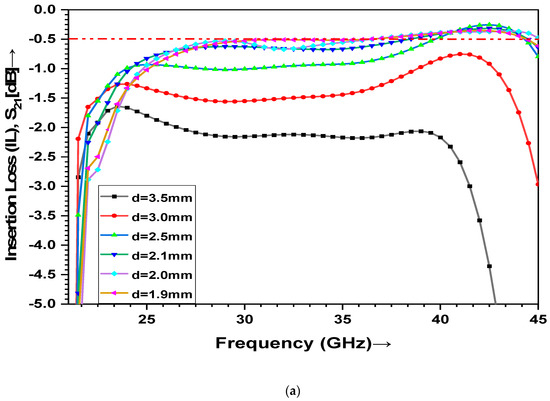
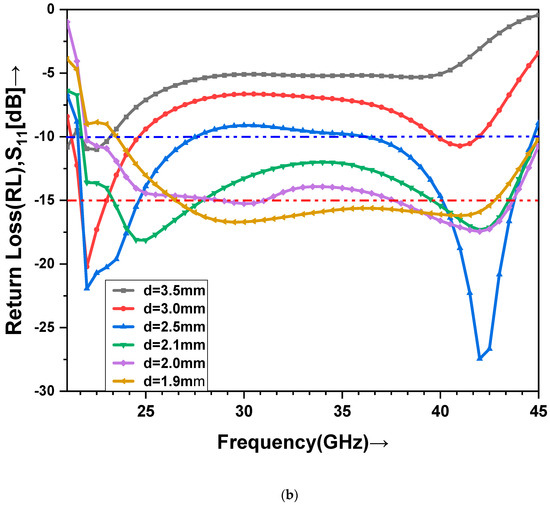
Figure 3.
Effect of back-short distance variations on (a) IL and (b) RL.
Table 2.
Effect of fish-tail width variations with HSlot = 3 h.
3.4. Optimization of Slot Height
The waveguide slot height is usually chosen as more than two times the substrate height. The effect of a slot height, HSlot, less than two times the substrate height, 2 × h (1.5 × h = 0.1905 mm), and a slot height greater than twice the substrate height (0.254/0.381/0.508 mm) was optimized while keeping the back-short distance constant, i.e., d = 1.9 mm. It was found that when HSlot < 2 h, a deviation in resonance frequency was observed, whereas when HSlot > 2 h, in all cases, resonance occurred close to the designed center frequency of 30 GHz, with better performance parameters in terms of RL, IL, and −10 dB absolute bandwidth, as shown by the family curves of IL and RL in Figure 4 and tabulated in Table 3. The optimized minimum value of the slot height was 0.381 mm, for which resonance occurred at a frequency of 29.75 GHz, with a much flatter RL below −15 dB over a wide bandwidth. It was noticed that with slot height, HSlot, greater than or equal to 3 times the substrate height, the return loss value was below −15 dB over a ultra-wideband. However, as the slot height was increased over 3.5 h, the RL went above −15 dB, which demonstrated an increase in reflections from the back-short and a reduction in transmission power. It was concluded from the two-parameter variations that variation of the back short distance and slot height affected each other and hence affected the RL, IL, and, therefore, the ultra-wide bandwidth. Therefore, a higher value of back-short distance led to decrease in slot height, and a lower value of back-short distance gives an increase in slot height. The dependency of these two important dimensions necessitates keeping one dimension constant; say the slot height equal to 2 h or 3 h, while changing the back-short distance for lower values of RL over a wider bandwidth.
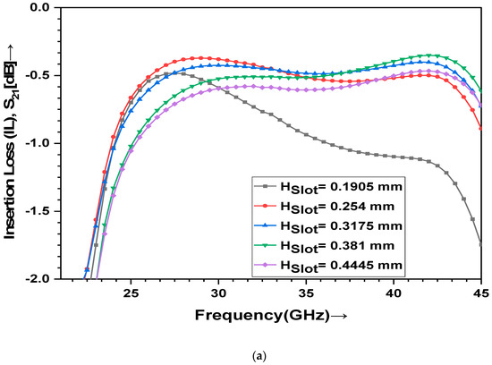
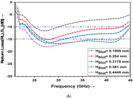
Figure 4.
Effect of slot height variations on (a) IL and (b) RL.
Table 3.
Effect of slot height variations with d = 1.9 mm.
3.5. Fishtail Probe Depth (LD) Optimization
A fish-tail-shaped probe was attached at the far end of the microstrip line and inserted into the waveguide WR-28. A 50 Ω excitation was applied at the near end. The fish-tail probe played an important role in impedance matching. The width and depth of the triangular-shaped probe were varied so that excellent impedance matching was achieved over the entire Ka-band. The depth of the fish-tail probe was varied in a step size of 0.20 mm in the direction of the marked arrow, as shown in Figure 5. Four depth increments from the substrate end were implemented, as signified in Figure 5 by the different colored tags. Corresponding insertion loss and return loss family plots are presented in Figure 6a,b. All variation effects on the absolute BW, RL, and IL are given in Table 4. It was observed that the lowest RL, highest −10 dB absolute bandwidth (BW), and minimum IL was obtained at a resonance frequency close to 30 GHz and with a fish-tail depth, LD, equal to 2.5 mm. Therefore, the maximum energy transfer and minimum IL occurred at a design frequency with a 2.5 mm distance from the substrate end. It was concluded that an increase in the fish-tail depth from the substrate end or waveguide broadside wall resulted in a reduction in reflections and improved the transmission. For distances of LD equal to 1.9 mm/2.1 mm/2.3 mm the IL values were below −0.50 dB. An excellent IL above 0.50 dB was obtained with a fish-tail depth of 0.4 mm from the flat microstrip end over an ultra-wide bandwidth of 23.52–45.0 GHz.
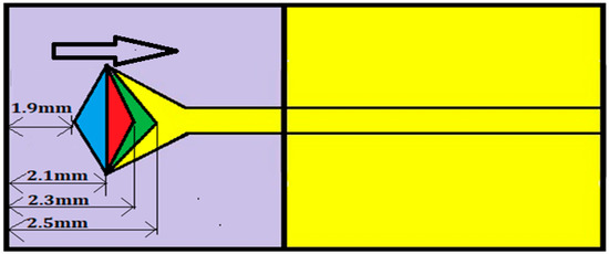
Figure 5.
Fish-tail depth variations with a step size of 0.2 mm from the substrate end.
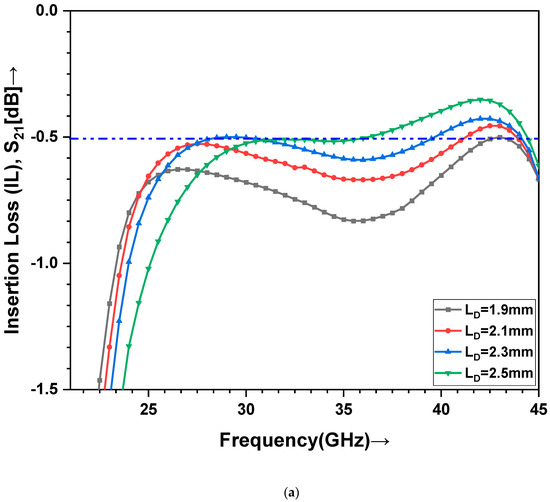
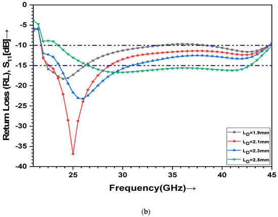
Figure 6.
Effect of fishtail depth variations on (a) insertion loss, S21 (dB), (b) return loss, S11 (dB).
Table 4.
Effect of fish-tail depth variations with a fish-tail probe width WP = 3.8 mm.
3.6. Fishtail Probe Width (WP) Optimization
The width of the fish-tail probe was varied in a step size of 0.4 mm symmetrically about the strip center line, as shown in Figure 7, and the corresponding effects of width variations on the IL and RL are plotted in Figure 8a,b, respectively, with a constant fish-tail depth of 2.5 mm. The effect of the variation of width on the IL, RL, and −10 dB absolute bandwidth is tabulated in Table 5. It can be observed from the table that, as the width of the fish-tail increases, the resonance (29.75 GHz) is close to the design frequency of 30 GHz, with a minimum IL −0.36 dB, RL −16.72 dB, and −10 dB absolute bandwidth 21.50 GHz being obtained. It can also be concluded from the tabular data that as the fish-tail probe width (WP) decreased, the insertion loss and return loss improved with a shift in the resonance frequency towards the Q-band and U-band upper-frequency limits. Therefore, the same transition could be easily and efficiently used for other than Ka-band microwave and millimeter wave applications, just by reducing the fish-tail probe width.
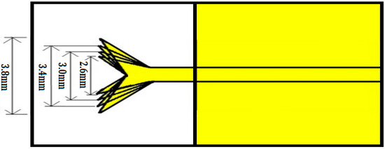
Figure 7.
Fish-tail width variation with a step size of 0.4 mm.
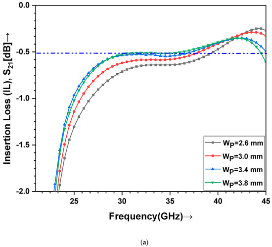
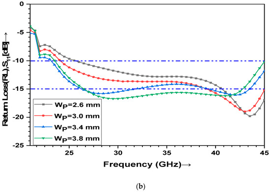
Figure 8.
Effect of fish-tail width on (a) insertion loss, S12 (dB) and (b) return loss, S11 (dB).
Table 5.
Effect of fish-tail width variations with a fish-tail depth = 0.4 mm.
4. Results and Discussion
4.1. Ka-Band RWG-to-Fish-Tail-Shaped MSL Design Model
A 3D Model of the final designed and optimized Ka-band microstrip line-to-WR-28 transition, including the outer embodiment, is displayed in Figure 9a. Photographs of the WR-28 with a back-short [17], along with front and rear views of the fabricated nature-inspired fish-tail-shaped microstrip lines are shown in Figure 9b. A 50 Ω microstrip line was fabricated on Roger’s RT Duroid 5880 soft substrate using photolithography and chemical etching processes. A 50 Ω connector was soldered at the strip end. The other end of the MSL was very close to the shape of a fishtail, as displayed by the arrow mark.
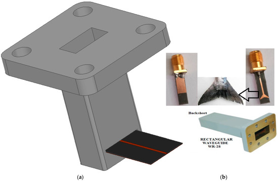
Figure 9.
(a) Ka-band RWG-to-MSL transition model, (b) prototype of the nature-inspired fish-tail microstrip line.
4.2. Optimized S-Parameters, VSWR, and Propagation Constant Plots of the Proposed Transition Model
The optimized S-parameters, in terms of the return loss and insertion loss, are depicted in Figure 10a, and the corresponding VSWR plot with frequency is displayed in Figure 11b. Figure 10a shows the minimum insertion loss of −0.36 dB and lowest return loss of −16.72 dB at a frequency of 29.75 GHz. A 66.15% fractional bandwidth was achieved for the concerned Ka-band structure. The −10 dB return loss with VSWR between the two ports of transition was 1.10, as shown in Figure 10b, demonstrating the good transmission of power flow between the two ports of the waveguide and microstrip line. The lowest insertion loss of −0.36 dB and return loss of −21.135 dB were obtained at the frequency 40 GHz. The transition exhibited return loss below −10 dB and an insertion loss below −0.50 dB for a 66.15% fractional bandwidth from 23.52 to 45.0 GHz. The attenuation constant, α, and phase constant, β, plots of real and imaginary parts of the propagation constant are displayed in Figure 10c. The phase constant was higher and attenuation went down to almost zero with a cut-off frequency of 21.25 GHz for the dominant TE10 mode. This shows that the proposed model covers some portions of the K-band (23.52–26 GHz out of the 18–26 GHz band), Q-band (33–45 GHz out of the 33–50 GHz band), and U-band (40–45 GHz out of the 40–60 GHz band), along with the entire Ka-band (26–40 GHz) application coverage. Ideally, the cut-off frequency is 21.09 GHz. Thus, only a 0.753% relative error in cut-off frequency was recorded. The zero attenuation constant value after the cutoff frequency guarantees that the designed transition model has extremely low losses and provides the highest transmission of EM power between the MS Line and RWG.
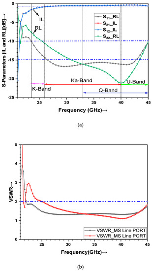
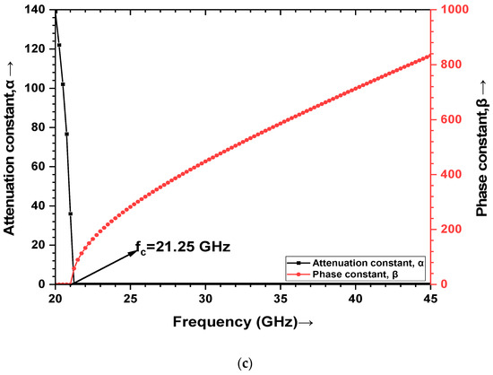
Figure 10.
RWG-to-MSL transition results at 30 GHz: (a) IL and RL plots, (b) VSWR plot, and (c) propagation constant plots.
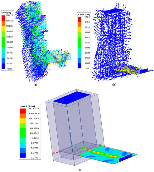
Figure 11.
(a) Electric field (E) distribution in transition, (b) magnetic field (H) distribution in transition, and (c) conduction current density (J) distribution in transition at 30 GHz.
4.3. Electric Field (E), Magnetic Field (H), and Surface Current Density (J) Distribution Inside the Designed Transition
The simulated electric field (E), magnetic field (H), and current density distribution (J) inside the WR-28-to-MSL transition at a frequency of 30 GHz for the design optimized parameters and dimensions are displayed in Figure 11a–c, respectively. It is clear from the field distribution that the field alters its direction after traveling λg/2 and repeats after traveling a distance of λg. This ensures that the length of the standard RWG (WR-28) provides a better transmission and low insertion when it is of the order of nearly an integer multiple of the half-guided wavelength (λg/2). The confined electric field within the transition also ensures that perfect matching between the quasi-TEM mode of the 50 Ω microstrip line and the nearly 500 Ω dominant mode (TE10) of WR-28 is achieved.
4.4. RLC Electrical Equivalent Circuit of the Transition
The RLC electrical T-equivalent and π-equivalent circuits of the fish-tail-shaped microstrip line to rectangular waveguide (WR-28) transition are depicted in Figure 12a,b, respectively. Corresponding to the sharp resonant frequency in the −10 dB bandwidth, as shown in Figure 10a, with minimum return loss values, all S-parameters are recorded and then converted into the corresponding equivalent Z-parameters and Y-parameters [14,18,19], and then these Z- and Y-parameters are converted into the T-equivalent and π-equivalent parameters [14,20]. Finally, the lumped RLC parameters are evaluated by comparing each T-equivalent parameter with Z = R + jX and π-equivalent parameters with Y = G + jB. Where, G and B are the corresponding conductance and susceptance, respectively [14]. The reciprocal of the conductance gives the value of R. The L and C are estimated from B at resonance conditions. Finally, the two T-equivalent and π-equivalent RLC electrical equivalent networks are realized in series and parallel, and then implemented in a single equivalent circuit in the proposed two-port E-plane transition [14,21,22,23,24].
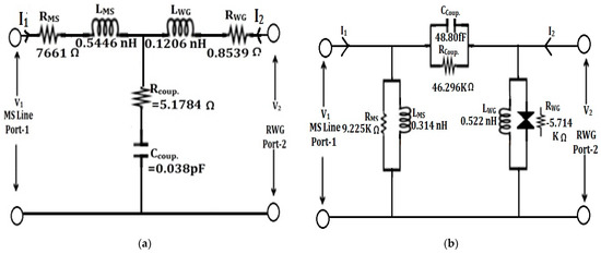
Figure 12.
RLC electric equivalent circuit of E-plane microstrip-to-WR28 transitions at 30 GHz: (a) T-equivalent circuit, (b) π-equivalent circuit.
4.5. Comparison of the Proposed Work with the Existing Ka-Band RWG-to-MSL Transitions
A parametric comparison of the performance results of the existing Ka-band MSL-toRWG transitions with the proposed Ka-band optimized design is shown in Table 6.
Table 6.
Ka-band Rectangular Waveguide to Microstrip Line Transition Design Results.
5. Conclusions
A simple, small, via-less, impedance-transformer-less, side inserted, E-plane transverse, 90° hybrid, rectangular waveguide to fishtail-shaped microstrip line transition for Ka-band millimeter wave, wireless, satellite, and RADAR applications was optimized and investigated in the simplest manner possible. It provides a good transmission from the microstrip line end port to the waveguide port end and vice versa. An insertion loss of less than 0.50 dB and return loss lower than −15 dB were achieved with an ultra-wideband fractional bandwidth of 66.15% of the chosen band of interest, with a lower than −10 dB bandwidth. The tapered microstrip line probe inside the rectangular waveguide WR-28 adopts a fishtail-like structure and provides very good impedance matching, and thus the maximum electromagnetic energy flow between rectangular waveguide and microstrip transmission lines, with extremely low losses (3% reflections only). This design eliminates the need for the previously existing Ka-band rectangular waveguides to microstrip line transitions, consisting of composite multi-section impedance transformers, tapered/exponential transformers, Chebyshev transformers, bow-tie structures, and circular and semicircular patch structures, etc. These features make this transition the most compact and simplest available and the most suitable for RADAR, wireless, and satellite communication applications. The proposed transition could form an essential part of MIC/MMIC-based circuits and systems, to interconnect with transmitter and receiver front ends, as well as waveguide components and structures. In the future, the bandwidth of the designed Ka-band transition could be increased through the use of advanced techniques, such as using a metamaterial split ring resonator/complementary split ring resonator and fractal geometries of the microstrip antenna insertion in the rectangular waveguide. The equivalent RLC circuits of the proposed transition model enable its use with any planar circuit or system. This transition, not only covers the Ka-band, but also could be suitable for use in applications with the K-band (23.52 GHz to 26 GHz), Q-band (33 GHz to 45 GHz), and U-band (40 GHz to 45 GHz).
Author Contributions
Conceptualization, A.V. and V.S.; methodology, A.V. and C.N.; software, A.V., C.N. and A.K.G.; validation, A.V. and V.S.; formal analysis, A.V. and Y.M.; investigation, A.V., V.S. and Y.M.; resources, A.V.; writing—original draft preparation, A.V.; writing—review and editing, A.V., A.K.G. and Y.M.; visualization, V.S. and C.N.; supervision, V.S.; funding, Y.M. All authors have read and agreed to the published version of the manuscript.
Funding
The authors would like to acknowledge the research funding to the Innovative Technologies Laboratories (ITL) from King Abdullah University of Science and Technology (KAUST).
Data Availability Statement
The authors declare that all data are provided in the article.
Acknowledgments
The authors would like to express their sincere thanks to the Honorable, GK (DU), Haridwar, Uttarakhand, India, for his motivation and encouragement regarding the research and for providing the simulation and laboratory environment for conducting this research work.
Conflicts of Interest
The authors declare no conflict of interest.
References
- Varshney, A.; Sharma, V. A comparative study of microwave rectangular waveguide-to-microstrip line transition for millimeter wave, wireless communications, and radar applications. Microw. Rev. 2020, 26, 21–37. [Google Scholar]
- Iffat Naqvi, S.; Hussain, N.; Iqbal, A.; Rahman, M.; Forsat, M.; Mirjavadi, S.S.; Amin, Y. Integrated LTE and Millimeter-Wave 5G MIMO Antenna System for 4G/5G Wireless Terminals. Sensors 2020, 20, 3926. [Google Scholar] [CrossRef] [PubMed]
- Li, J.; Xu, J.; Fu, J.A. Full Ka-band microstrip to-waveguide transition using side-inserted magnetic coupling semicircular ring. In Proceedings of the Wamicon 2012 IEEE Wireless and Microwave Technology Conference, Cocoa Beach, FL, USA, 15–17 April 2012; pp. 1–6. [Google Scholar]
- Shih, Y.C.; Ton, T.N.; Bui, L.Q. Waveguide-to-microstrip transitions for mm-wave applications. IEEE MTT-S Int. Symp. Dig. 1988, 1, 473–475. [Google Scholar]
- Tomar, S.; Singh, S.K.; Suthar, L.; Singh, R.B.; Kumar, A. E-Plane waveguide to microstrip transition for wave applications. In Proceedings of the Conference ICMARS, Jodhpur, India, 14–17 December 2010; pp. 1–3. [Google Scholar]
- Varshney, A.K.; Rawat, G.S. A microwave rectangular waveguide-to-microstrip line transitions @ 30 GHz. Int. J. Emerg. Technol. Adv. Eng. 2013, 3, 563–568. [Google Scholar]
- Lou, Y.; Chan, C.H.; Xue, Q. An in-line waveguide-to-microstrip transition using a radial-shaped probe. IEEE Microw. Wirel. Compon. Lett. 2008, 18, 311–313. [Google Scholar] [CrossRef]
- Varshney, A.K.; Sharma, V. Using a reverse approach to obtain an efficient design for a wideband MS line-RWG hybrid transition. In Proceedings of the International Conference on Emerging Trends in Applied Sciences, Virtual, 28–29 October 2021. [Google Scholar]
- Tang, C.; Pan, X.; Cheng, F.; Lin, X.A. Broadband microstrip-to-waveguide end-wall probe transition and its application in Waveguide Termination. Prog. Electromag Res. Lett. 2020, 89, 99–104. [Google Scholar] [CrossRef]
- Li, C.L.; Jin, C.; Ma, H.Q.; Shi, X.W. An Inline Waveguide-to-Microstrip Transition for Wideband Millimeter-wave Applications. Microw. Opt. Technol. Lett. 2019, 62, 1516–1520. [Google Scholar] [CrossRef]
- Gupta, R.; Kumar, P.P. Improved Design of Ka-band Waveguide to Coaxial Right Angle Microwave Transition. In Proceedings of the URSI RCRS 2020, IIT (BHU), Varanasi, India, 12–14 February 2020. [Google Scholar]
- Simone, M.; Fanti, A.; Valente, G.; Montisci, G.; Ghiani, R.; Mazzarella, G. A Compact In-Line Waveguide-to-Microstrip Transition in the Q-Band for Radio Astronomy Applications. Electronics 2018, 7, 24. [Google Scholar] [CrossRef]
- Lim, Y.Y.; Goh, Y.M.; Yoshida, M.; Bui, T.T.; Aoyagi, M.; Liu, C. 30-GHz High-Frequency Application of Screen Printed Interconnects on an Organic Substrate. IEEE Trans. Compon. Packag. Manuf. Technol. 2017, 7, 1506–1515. [Google Scholar] [CrossRef]
- Pozar, D.M. Microwave Engineering, 4th ed.; Wiley Student Edition; John Wiley and Sons: Hoboken, NJ, USA, 2016; pp. 148–149. [Google Scholar]
- Liao, S.Y. Microwave Devices and Circuits, 3rd ed.; Pearson Prentice Hall: Hoboken, NJ, USA, 2007; pp. 120–137. [Google Scholar]
- Chang, K. RF and Microwave Wireless Systems; John Wiley and Sons: Hoboken, NJ, USA, 2015; pp. 90–99. [Google Scholar]
- ESATCOM INC. WR-28 Waveguide Termination. 1995. Available online: https://esatcom.com/waveguideterminations/1360-WR-28-waveguidetermination.html (accessed on 26 May 2022).
- Varshney, A.; Cholake, N.; Sharma, V. Low-cost ELC UWB fan-shaped antenna using parasitic SRR triplet for ISM band and PCS applications. Int. J. Electron. Lett. 2021, 10, 391–402. [Google Scholar] [CrossRef]
- Varshney, A.; Sharma, V.; Arya, V. Tri-Blade Table Fan-Shaped Ultra-Wideband Microstrip Antenna Using Parasitic SRR Triplet. Australian Patent No. 2021101898, 19 May 2021. [Google Scholar]
- Choudhary, D.R. Networks and Systems, 12th ed.; New Age International Publishers: Delhi, India, 1999; pp. 432–484. [Google Scholar]
- Varshney, A.; Sharma, V.; Shrivastava, A. A Novel Simplified Equivalent Modeling for Microstrip Line Interconnects. Indian Patent No. 202111019468, 7 May 2021. [Google Scholar]
- Shireen, R.; Shi, S.; Prather, D.W. W-band microstrip-to-waveguide transition using via fences. Prog. Electromagn. Res. Lett. 2010, 16, 151–160. [Google Scholar] [CrossRef]
- Tong, Z.; Stelzer, A. A vertical transition between rectangular waveguide and coupled microstrip Lines. IEEE Microw. Wirel. Compon. Lett. 2012, 22, 251–253. [Google Scholar] [CrossRef]
- Varshney, A.; Sharma, V.; Elfergani, I.; Zebiri, C.; Vujicic, Z.; Rodriguez, J. An Inline V-Band WR-15 Transition Using Antipodal Dipole Antenna as RF Energy Launcher @ 60 GHz for Satellite Applications. Electronics 2022, 11, 3860. [Google Scholar] [CrossRef]
Disclaimer/Publisher’s Note: The statements, opinions and data contained in all publications are solely those of the individual author(s) and contributor(s) and not of MDPI and/or the editor(s). MDPI and/or the editor(s) disclaim responsibility for any injury to people or property resulting from any ideas, methods, instructions or products referred to in the content. |
© 2023 by the authors. Licensee MDPI, Basel, Switzerland. This article is an open access article distributed under the terms and conditions of the Creative Commons Attribution (CC BY) license (https://creativecommons.org/licenses/by/4.0/).