Abstract
In the clock network design, the trade-off between power consumption and timing closure is an important and difficult issue. The clock tree architecture has a shorter wire length and better power consumption, but it is more difficult to achieve timing closure with it. On the other hand, clock mesh architecture is easier to satisfy the clock skew constraint, but it usually has much more power consumption. Therefore, a hybrid clock network architecture that combines both the clock tree and clock mesh seems to be a promising solution. In a normal hybrid mesh/tree structure, a driving buffer is placed in the intersection of mesh lines. In this paper, we propose a novel cross-mesh architecture, and we distribute the buffers to balance the overall switching capacitance, reducing the number of registers connected to a subtree, and the load capacitance of a buffer. With the average dispersion of the overall driving force, our methodology creates small non-zero skew clock trees. In addition, we integrate clock gating, register clustering, and load balancing techniques to optimize clock skew and load capacitance simultaneously. The proposed methodology has four stages: cross-mesh planning, register clustering, mesh line connecting, and load balancing. Experimental results show that our cross-mesh architecture has high tolerance for process variation, and is robust in all the operation modes. Comparing it to the uniform mesh architecture, our methodology and algorithms reduce 28.9% of load capacitance and 80.4% of clock skew on average. Compared to the non-uniform mesh architecture, we also reduce capacitance by 22.4% and skew by 76.7% on average. This illustrates that we can obtain a feasible solution effectively and improve both power consumption and clock skew simultaneously.
1. Introduction
In the design of a synchronous circuit, a clock signal ideally must propagate to all components at the same time. However, since the distance from the clock source to all sequential elements is different, there exists a timing difference between these clock signal paths. A circuit with a large clock skew will cause a failure of its functionality. With the increasing complexity of high-performance chip design and process variation, clock network synthesis becomes a crucial and difficult problem.
There are three important issues in the modern clock network synthesis problem: clock skew, process variation, and power consumption. To satisfy these considerations, clock tree and clock mesh are the two commonly used clock network synthesis approaches. Comparing these two approaches, the clock tree network has a shorter wire length and better power consumption, but it is more difficult to achieve timing closure with it and it has less tolerance for process variation. On the other hand, the clock mesh network has higher tolerance for process variation and makes it easier to satisfy the clock skew constraint, but it usually has much more power consumption.
Because of the tight clock skew constraint, process variation tolerance, and low power requirement of high-performance circuit design, the concept of a hybrid clock network was proposed in recent years. This style of clock network architecture aims at integrating both the lower power advantage of the clock tree and the easy timing convergence of a clock mesh, such that timing closure and an optimization of power consumption can be achieved simultaneously.
Recently, machine learning and fuzzy inference methods are also used to solve this problem, but it seems we still have a long way to reach promising solutions. The algebraic formulation of fuzzy relation is studied in [,].
In this paper, we propose a new cross-mesh architecture. In a normal hybrid mesh/tree structure, the clock mesh layout is based on the board shape, and the driving buffer is placed in the intersection of mesh lines. For example, Figure 1a is a 2 × 2 sized uniform clock mesh design, in which the driver buffer is placed in the mesh line intersection to drive the registers within the mesh, and its driving range is shown by the gray rectangle. In contrast, our proposed cross-mesh layout is as shown in Figure 1b. The range of a driving buffer is changed from the original rectangular area to one that is cut into four triangular areas. We use this mesh architecture to distribute the buffers to balance the overall switching capacitance, reducing the number of registers connected to a subtree, and the load capacitance of a buffer.
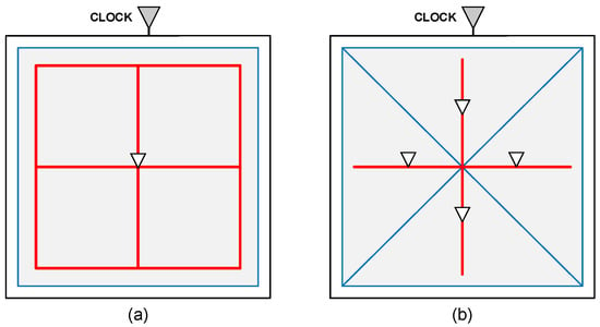
Figure 1.
(a) Uniform clock mesh. (b) Cross-clock mesh.
The advantage of cross-mesh architecture is illustrated below. We assume that the capacitance and power consumption of every piece of wire is 1 pf and 1 pw, the 1X buffer has 4 pf of capacitance and 4 pw of power consumption, and the 4X buffer has 10 pf of capacitance and 10 pw of power consumption. In this example, a uniform clock mesh is composed of twelve nets and one 4X buffer, the total power consumption is 12 × 1 + 10 = 22 pw, and the total capacitance is 12 × 1 + 10 = 22 pf.
On the other hand, the cross-clock mesh uses four buffers as driving buffers to drive an area of the same size, and each driving buffer on average only drives the triangular area surrounded by blue lines which is equal to one-fourth of the original area. This change can reduce the output capacitance of the driving buffer, and hence timing convergence will be easier to achieve.
There are four 1X buffers and four pieces of wire in the circuit. The total capacitance can be calculated as 4 × 1 + 4 × 4 = 20 pf, and the power consumption is 4 × 1 + 4 × 4 = 20 pw. In this example, we show that the cross-mesh not only has smaller capacitance but also less power consumption in comparison with the uniform mesh.
Based on the proposed hybrid clock network architecture, we also integrate clock gating, register clustering, and load balancing techniques to optimize clock skew and load capacitance simultaneously.
The rest of this paper is organized as follows. Section 2 describes related work on the clock tree, clock mesh, and hybrid network. Section 3 illustrates our motivation for integrating the cross-mesh architecture, clock gating and load balancing techniques in the local clock tree with an example. In Section 4, we propose a four-stage methodology for hybrid cross-mesh synthesis: cross-mesh planning, register clustering, mesh line connecting, and load balancing. Experimental results in Section 5 show the robustness of the proposed clock network architecture and the effect of integrating these optimization techniques. Finally, we provide the concluding remarks in Section 6.
2. Related Works
2.1. Clock Tree
Buffer insertion, buffer sizing, and wire sizing are the most common techniques for the minimization of clock skew in clock tree synthesis [,,,,], while in multi-voltage mode designs, the insertion of adjustable delay buffers (ADBs) and value adjustment are commonly used to resolve the clock skew problem. Su et al. [,] proposed a linear-time algorithm to assign delay values of ADBs for clock skew optimization on all power modes. Lim et al. [] and Kim et al. [] proposed complete solutions for clock skew optimization under multiple power modes, including the minimum number of ADBs required, allocation of ADBs, and delay value assignment of each ADB in each power mode.
In modern VLSI Design, on-chip-variation (OCV) becomes serious as the feature size shrinks continuously. Kao et al. [] present a practical industrial design methodology for minimizing the OCV-induced clock skew of the top-level clock tree; the basic idea is to pre-place guide buffers for clock tree synthesis so that wire lengths of non-common paths can be reduced.
In addition to the minimization of clock skew, reducing the power consumption of the clock network is another important issue, and clock gating is a widely used technique. The location of a clock gate and the number of registers it drives have a large impact on both the power consumption and the clock signal delay. Teng and Soin [,] proposed a clock gate splitting methodology to improve time convergence and increase the setup time region. They also integrated splitting and merging techniques to find the optimum location of clock gates. Wang and Roy [] proposed a graph-based algorithm for the clock root gating problem. Shelar [] proposed a clustering method to reduce the number of buffers and power consumption. Chan et al. [] proposed a linear programming methodology to minimize power consumption, wire length, and timing slew simultaneously. Lin et al. [] proposed an activity-driven clock tree design methodology, including a new tree structure and a corresponding design flow. Cheng et al. [] proposed a skew-window-based methodology to reduce the total hardware cost of ADBs and clock gates simultaneously. Lin et al. [] present a general activity-driven clock tree structure in which both the AND gate and OR gate can be utilized at any node. Based on this general structure, an effective synthesis algorithm is proposed.
2.2. Clock Mesh
Most research on clock mesh synthesis targeted reducing the power consumption of stub wires, including wire length reduction, mesh size tuning, and using a non-uniform mesh size. Lu et al. [,] proposed ILP (integer linear programming) formulations for register clustering, where registers at neighboring locations with similar switching activities are grouped into one cluster to reduce wire length. They also proposed an ILP solution to move registers more closely to mesh wires and hence reduce the length of stub wires. In addition, Lu et al. [] proposed a binary search algorithm to find the suitable mesh size under the constraints of mesh size and register displacement. Venkataraman et al. [] proposed a greedy algorithm that selects the drive buffer location and size to reduce the overall drive buffer hardware cost, and Liu et al. [] proposed a clock mesh design with wire sizing optimization.
In contrast to the uniform mesh structure, a non-uniform mesh can reduce both the length of mesh wires and stub wires by adjusting the position of mesh wires. Abdelhadi et al. [] proposed a graph-based non-uniform mesh methodology to reduce power consumption by planning more mesh wires in critical timing paths, and fewer mesh wires in non-critical timing paths. Guthaus et al. [] iteratively moved the position of mesh wires until the length of mesh wires and stub wires was minimized. Cho et al. [] proposed binary linear programming formulations for clock mesh synthesis and register assignment such that the capacitance of registers and stub wires could be balanced. Cheng et al. [] proposed a methodology to reduce switching capacitance via non-uniform clock mesh synthesis, clock gate insertion, and register clustering. Yang and Huang [] proposed an ILP approach to reduce the wire length of a non-uniform clock mesh under temperature constraints.
2.3. Hybrid Network
Hybrid network aims at integrating both the benefit of the clock tree and clock mesh. In [], various clock network architectures are introduced, in which the hybrid clock architecture is divided into two categories, namely the upper clock mesh with the local clock tree (MLT) and the upper clock tree with the local clock mesh (TLM). Su and Sapatnekar [] constructed a hybrid mesh/tree clock network structure consisting of overlying zero-skew clock meshes, with underlying zero-skew clock trees originating from the mesh nodes. Chen et al. [] focus on the performance and optimization of a multi-source CTS flow which applies a coarse mesh with local subtrees. They proposed several heuristic approaches to improving the performance of multi-source CTS, especially for skew optimization. In [], with a combination of non-uniform meshes and un-buffered trees, a variation-tolerant hybrid clock distribution network was produced. Clock skew variations were selectively reduced based on the circuit timing information generated via static timing analysis. Xiao et al. [] proposed a hybrid method that creates a mesh upon a tree topology. A clock mesh was built first according to the positions and capacitance of the sinks. A top-level tree was then built to drive the mesh. A blockage-aware routing method was used during tree construction.
In this paper, we propose a novel cross-mesh architecture; with the average dispersion of the overall driving force, our methodology creates small non-zero skew clock trees and reduces the usage of clock gates. We also propose clock gating, register clustering, and load balancing algorithms to optimize both clock skew and load capacitance simultaneously. Experimental results show that our approach is robust and effective.
3. Motivation Example
The example in Figure 1 illustrates the influence of the driving buffer’s location and the mesh wire’s connection on load capacitance and power consumption, and the advantage of cross-mesh architecture. In this section, we further illustrate the reasons for applying clock gating and load balancing techniques on the local clock tree, and analyze the capacitance and power consumption of register clusters in each kind of subtree topology. Through the example in Figure 2a–c, we illustrate how clock gating and load balancing techniques can reduce the capacitance load on mesh wires. Figure 2d illustrates how we integrate these two optimization techniques into the cross-mesh architecture to further reduce the capacitance load. Details of this example are described below.
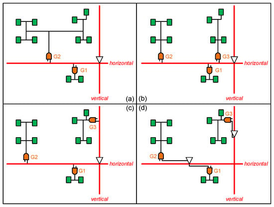
Figure 2.
Motivation example (a) mesh tree (b) clock gating on mesh tree (c) load balancing on mesh tree (d) cross-mesh with clock gating and load balancing.
The switching capacitance and power consumption of a register cluster are defined in Equations (1) and (2).
Capmesh_wire is the wire’s capacitance from the driving buffer to the gate that is the beginning of a register cluster, Capgate is the capacitance of a cluster gate, Capsubtree_wire is the wire capacitance in a cluster, and Capreg is the capacitance of a register. Because we use a clock gate to control a register cluster, it needs a parameter, α, to represent the activity ratio of a cluster. If , it means this cluster will activate half of the time during the working process. To simplify the problem, we assume that the α of every gate is 0.5 in this example. Note that parameters of power are similar to those of capacitance, while for the other parameters, we assume that the capacitance and power of the 1X gate is 6 pf and 6 pw, and those of 4X gate is 14 pf and 14 pw. Similarly, we assume that the capacitance and power of a register is 5 pf and 5 pw.
In Figure 2a, circuit A is a conventional mesh tree which branches into two clusters. For cluster 1, we assume that Capmesh_wire = 5 pf and Pwrmesh_wire = 5 pw, and Capsubtree_wire = 5 pf and Pwrsubtree_wire = 5 pw. Therefore, and . For cluster 2, we assume that Capmesh_wire = 10 pf and Pwrmesh_wire = 10 pw, and Capsubtree_wire = 30 pf and Pwrsubtree_wire = 30 pw. Therefore, and . In cluster 2, there are eight registers in the tree topology; thus, it needs to use a 4X gated cell to drive the clock tree. At last, the average capacitance is 33.75 pf and total power consumption is 62.5 pw. Incidentally, Pwrmesh_wire1 is public in clusters 1 and 2, and we only need to calculate it one time for total power consumption.
For the conventional mesh tree in Figure 2a, there are two optimization methods to reduce capacitance load. For the first optimization method, because cluster 2 is too large to drive by a gate, we insert another gate, G3, to divide cluster 2 into two smaller clusters like the mesh tree in Figure 2b. This method not only mitigates the capacitance of each gate (in other words, a large gate can be instead replaced by a smaller one), but also increases the possibility of timing closure due to more balance between clusters. In Figure 2b, we assume that the Capmesh_wire and Pwrmesh_wire values of clusters 1, 2, and 3 are 5 pf, 13 pf, and 4 pf, and 5 pw, 13 pw, and 4 pw; the Capsubtree_wire and Pwrsubtree_wire values are 5 pf, 13 pf, and 14 pf, and 5 pw, 13 pw, and 14 pw. Using Equations (1) and (2), we can obtain the Captot values of clusters 1, 2, and 3, which are 15.5 pf, 32.5 pf, and 24 pf, and the Pwrtot values of clusters 1, 2, and 3 are 15.5 pw, 32.5 pw, and 24 pw. The average capacitance of this mesh tree is 24 pf and the total power consumption is 63 pw. This optimization method significantly reduces the average capacitance of the driving gate but only has 0.5 pw of extra total power.
The second optimization method aims at balancing the gate amount on all mesh wires. Actually, it is better to put all gates on the mesh wires on average to reduce the maximum loading, since too much loading on a mesh wire will induce a timing as well as thermal problem in the circuit. For the mesh tree in Figure 2c, we assume that the Capmesh_wire and Pwrmesh_wire values of clusters 1, 2, and 3 are 5 pf, 13 pf, and 8 pf, and 5 pw, 13 pw, and 8 pw; the Capsubtree_wire and Pwrsubtree_wire values are 5 pf, 13 pf, and 14 pf, and 5 pw, 13 pw, and 14 pw. Using Equations (1) and (2), we obtain the Captot values of clusters 1, 2, and 3, which are 15.5 pf, 32.5 pf, and 28 pf, and the Pwrtot values of clusters 1, 2, and 3 are 15.5 pw, 32.5 pw, and 28 pw. The average capacitance of this mesh tree is 25.3 pf and the total power consumption is 71 pw. Compared to the mesh tree in Figure 2b, it has a little increase in both average capacitance and total power consumption. However, if we only focus on the horizontal mesh wire, it has better average capacitance and total power consumption values which are 24 pf and 43 pw due to cluster 3 being connected to the vertical mesh wire.
Finally, the mesh tree in Figure 2d is different from that of the two previous methods, and we use the proposed cross-mesh architecture to build the mesh tree. Despite the mesh tree in Figure 2c balancing the loading of mesh wires, the burden of driving buffers is still the same. To resolve this problem, our proposed method puts driving buffers on both the x-axis mesh and y-axis mesh. This means that gate cells in the clusters will connect to the mesh tree on average through these guide buffers. We assume that the Capmesh_wire and Pwrmesh_wire values of clusters 1, 2, and 3 are 4 pf, 5 pf, and 3 pf, and 4 pw, 5 pw, and 3 pw; the Capsubtree_wire and Pwrsubtree_wire values are 5 pf, 13 pf, and 14 pf, and 5 pfw 13 pw, and 14 pw; the Pwrmesh_wire values of buffer12 and buffer3 are 8 pw and 5 pw. Using the equations, we obtain the Captot values of of clusters 1, 2, and 3, which are 14.5 pf, 24.5 pf, and 23 pf and the Pwrtot values of clusters 1, 2, and 3 are 14.5 pw, 24.5 pw, and 23 pw. Because there are two driving buffers in the circuit, we analyze the average capacitance and total power consumption for each buffer. For buffer12, the average capacitance is 19.5 pf and total power consumption is 47 pw. On the other hand, the average capacitance and total power consumption values are 23 pf and 28 pw for buffer3. This result shows that our cross-mesh architecture can further reduce the capacitance load of each cluster. We cannot compare power consumption between the conventional mesh tree and the proposed cross-mesh tree here directly due to their different structures. Instead, we will discuss it in next paragraph the power consumption of the whole mesh tree.
To compare the average output capacitance to drive buffers and the total power consumption of the whole mesh tree between the four results in Figure 2, we assume that the power consumption of a driving buffer is 4 pw, and a piece of mesh wire is 18 pw. According to the mesh structure in Figure 1, there are twelve pieces of mesh wires in a conventional mesh structure, and only four pieces of mesh wires in the cross-mesh structure. Since all mesh trees in Figure 2 only use one-fourth of the whole mesh structure, we calculate four pieces of mesh wires for mesh trees in Figure 2a–c, and two pieces of mesh wires for the mesh tree in Figure 2d. In Table 1, Capavg in the subtree denotes the average capacitance of every cluster, while Capavg in the whole circuit is the average output capacitance to each driving buffer, and Pwrtot is the total power consumption of the whole circuit. In this table, we can see that cross-mesh structure has much better results than the three others do.

Table 1.
Result of our motivation example.
4. Design Flow and Methodology
4.1. Overview
There are four stages in our proposed methodology. As shown in Figure 3, our program reads a post-placement circuit to construct a cross-mesh tree. The first stage is cross-mesh construction and primary driving buffer placement, and we classify registers into groups according to the buffer driving range. The second stage is to insert a clock gate if necessary. We cluster registers into groups based on the cluster constraint to optimize the total capacitance, and determine the size and location of logic gates, then insert them to control the clusters. After that, the relationship between clusters is established, and the third stage is to connect each clock subtree to the drive buffer until they become a completed mesh tree. Finally, the fourth stage is to balance the load capacitance of each clock subtree; we evaluate all branches of the mesh tree and balance their capacitance to further minimize the clock skew between them. The detailed procedures of each stage are illustrated in the following subsections.
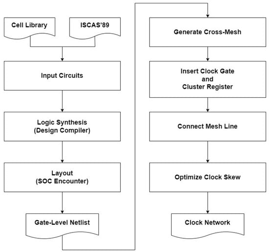
Figure 3.
Cross-mesh design flow.
4.2. Cross-Mesh Planning Algorithm
There are three steps in this stage: cross-mesh construction, driver buffer placement, and register classification. In the first step, we plan and construct the cross-mesh using the input file, which includes the chip’s structure and cells’ location. After that, we place drive buffers to suitable locations in the chip. At last, our program assigns registers to its best-fitting drive buffer according to the area of drive buffers and location of registers.
We use Figure 4 to illustrate our method; our program uses a core size in the chip to determine how to setup the mesh wire. The rectangular area of the core is represented by coordinates of the bottom-left (Corex1 and Corey1) corner and top-right corner (Corex2 and Corey2). We use Equations (3) and (4) to obtain the coordinate of the cross-mesh from the core information.
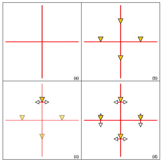
Figure 4.
Example of establishing cross-mesh (a) mesh wire (b) drive buffer on the center of mesh wire (c) additional drive buffers to make up the drive strength (d) completed mesh structure.
In Equations (3) and (4), Cross-Meshx and Cross-Meshy are coordinates of the cross-mesh. After completing mesh wire construction, we start to insert drive buffers in the mesh structure. For the example in Figure 4a, there are four directions of the wire in the tree (red line). At first, we put drive buffers on the center of each piece of mesh wire (orange triangle) as shown in Figure 4b. The mesh tree will use these four buffers to drive cells. Because the complexity of IC design grows drastically, it is insufficient to drive the cross-mesh using only four drive buffers. We divide the original triangular drive area in half using mesh wire as in Figure 4c, adding two additional drive buffers (white triangle) to make up the drive strength. The design with a completed mesh structure is as shown in Figure 4d.
After the first two steps, the third step is to classify registers and connect them to corresponding drive buffers. The judgement of classification is based on the Manhattan distance from the mesh wire to the register. That is, we can obtain a guaranteed result that has the smallest routing distance to reduce wire capacitance. We use the example in Figure 5a for illustration; this circuit has a mesh structure (red line), and there are four free registers (green rectangle) that need to be classified. In Figure 5b, we first choose a register to calculate and compare its distance to the horizontal and vertical mesh wires (purple dotted line). Obviously, it is near to vertical mesh wire; thus, the program assigns it to the drive buffer on the vertical mesh wire as shown by the blue line in Figure 5c. If a register has the same distance to the vertical and horizontal wires, we connect it to the drive buffer that has less registers connected to it as shown in Figure 5d. Note that if the number of connected registers is the same, our program appoints it randomly as shown in Figure 5e. We classify registers using this method iteratively until all registers have their corresponding drive buffer as shown in Figure 5f.
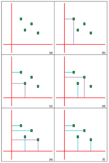
Figure 5.
Example of allocating driving buffer (a) four free registers to be classified (b) compare distance to mesh wires (c) connect to drive buffer with less distance (d) connect to drive buffer that has less registers connected to it (e) select drive buffer randomly on equal condition (f) completed allocation.
4.3. Register Clustering Algorithm
Although the previous stage classifies registers to their suitable drive buffers roughly, the number of connected registers for each drive buffer is still too large. Therefore, clustering these registers into groups and inserting more buffers to drive them are imperative. Figure 6 is the flow graph of this stage. Firstly, we treat each register as an individual cluster, and then our algorithm inserts a clock gate into each cluster. Note that we use the same type of clock gate in the optimization procedure to enhance the efficiency. Secondly, we use a greedy-like algorithm to merge clusters. For example, assume neighbored clusters Gi and Gj are selected. If the total capacitance of Gi and Gj is smaller than the limit of the load capacitance, clusters Gi and Gj will merge into a new cluster, Gv. This procedure continues until the total capacitance is over the threshold value. With this method, we can group registers rapidly with good results and satisfy design constraints.
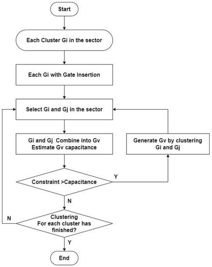
Figure 6.
Flow of register clustering algorithm.
Figure 7 is an example of our algorithm. There are five registers in this area (green rectangle); the red line represents the mesh wire and the grey line means these registers belong to the horizontal mesh wire. In Figure 7a, our program first treats each register as a cluster, and then inserts a clock gate into each cluster as shown in Figure 7b. After that, the distance between the pair of registers is determined to make sure that the merged clusters in the next step are neighbors. In Figure 7b, the two registers in the purple circle are near to each other and are chosen. We merge them into a cluster and continue to merge other clusters as shown in Figure 7c. Finally, we group registers into three clusters as shown in Figure 7d. This stage plays an important role in our whole design flow since better clustering brings out a better clock mesh tree structure. In other words, good clustering not only has lower power consumption but also better timing for closure achievement.
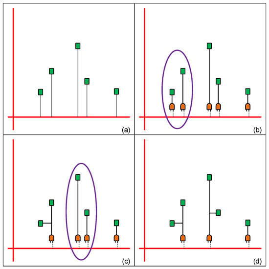
Figure 7.
Example of register clustering algorithm (a) each register is a cluster (b) two registers near to each other are chosen (c) merge chosen registers into a cluster and continue to merge other registers (d) completed register clustering.
4.4. Mesh Network-Connecting Algorithm
In this stage, we build a whole clock mesh tree by connecting the subtree we clustered in the previous stage to drive the buffer and inserting buffers between them if necessary. We use Equation (5) to calculate the output capacitance of each drive buffer, where is the total wire capacitance from the drive buffer to all clock gates; is the amount of clock gates. is the capacitance of a clock gate. If is too large for a drive buffer, group splitting is necessary to be performed to reduce capacitance. Thus, our algorithm will divide clusters into several groups and insert new buffers to help drive all clusters in this area. We continue this step iteratively until its capacitance meets the constraint.
We use an example to illustrate the mesh network-connecting algorithm; there is a drive buffer (white triangle) and four cluster of registers as shown in Figure 8a. In the beginning, we connect four clusters to the drive buffer directly, and hence the output capacitance of the drive buffer exceeds the constraint. Therefore, we divide a group into half and insert two drive buffers to help the original drive buffer as shown in Figure 8b. Then, our algorithm calculates their capacitance again as in Figure 8c; we find that these two new groups can all be driven by their drive buffer, and also the two new drive buffers can be driven by the original drive buffer. Finally, we connect all buffers and clock gates as shown in Figure 8d. After this stage, a clock mesh tree is established completely, but there is still design space to further optimize its timing issue as described in the next stage.
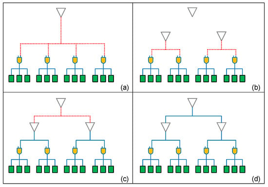
Figure 8.
Example of mesh network-connecting algorithm (a) original network (b) divide a group into half and insert drive buffers (c) check load capacitance and connect drive buffers (d) completed mesh network.
4.5. Load Balancing Algorithm
In this stage, we optimize the timing issue in two phases. The first phase is to optimize the timing difference between the clock gate subtrees. We use load matching technology to build the clock tree in order to make the clock skew close to zero. In order to make the load capacitance in each clock gate subtree closer, we insert dummy cells to make the delay of clock gates consistent. Figure 9 shows the load balancing algorithm. In the beginning, we first calculate the path delay and capacitance before optimization, find the clock gate subtree with the largest capacitance value, and set its capacitance value as the target capacitance value. Then, we select each clock gate subtree in order and compare its capacitance with the target capacitance value. If it is less than the target capacitance value, we calculate the difference and estimate how many dummy cells are needed to reach the target capacitance using Equations (6)–(8).
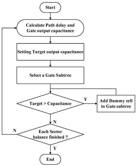
Figure 9.
Flow of load balancing algorithm.
Equation (6) is used to calculate the number of required dummy cells, Ndummy, where Ctarget is the target capacitance, Cbefore represents the clock gate load capacitance that does not have dummy cells inserted into it, and Cdummy is the capacitance value of the dummy cell. The additional capacitance value, Cextra, is calculated using Equation (7), and the load capacitance of the clock gate subtree is updated using Equation (8). We repeat these steps until all the clock subtree load capacitances are balanced.
The example in Figure 10 is a schematic diagram of a drive buffer connecting three clock gate subtrees. After calculating the load capacitance of each subtree, we assume the middle clock subtree in Figure 10a has the maximum load capacitance, we set this capacitance value as the target limit, and then add dummy cells one by one. In Figure 10b, we first process the left-hand clock subtree and calculate the number of dummy cells needed in accordance with the above equations. As shown in Figure 10c, adding a dummy cell to the left subtree can allow the value of the target capacitance to be matched, and then we process the clock subtree on the right. We repeat this method to add dummy cells until all clock subtrees are processed as shown in Figure 10d.
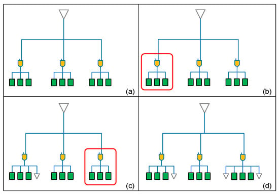
Figure 10.
Example of load balancing algorithm (a) original subtrees (b) the left subtree needs to add dummy cells (c) followed by the right subtree to add dummy cells (d) completed subtrees with load balanced.
5. Experiment Results and Discussion
We use testbenches (s9234, s13207, s38584, and s35932) in ISCAS’89 to test our algorithm; the number of registers in these testbenches is 211, 638, 1426, and 1728, respectively. For the purpose of comparing our work with other works fairly, we set up the same experiment environment as that of []. The target cell library is TSMC 90nm; we use Synopsys Design Compiler to obtain the gate-level netlist, and use Cadence SoC Encounter for the floorplan and placement.
We analyze our results and compare them with those of the works in [,] in terms of clock skew and capacitance values. Because the capacitance value is directly proportional to power consumption, and for the purpose of fair comparison, we provide capacitance value instead of power consumption in the table results.
5.1. Analysis of Cross-Mesh Clock Network
At first, we analyze the circuit optimized using our cross-mesh clock network. Table 2 presents the results on the amount of clock gates under different cluster constraints, where the cluster constraint is the percentage of the maximum affordable load capacitance downstream of a clock gate. Although the number of clock gates is smaller when there is ahigh constraint percentage, the slew of the signal may change much more easily due to the high load capacitance. In our method, the algorithm makes a tradeoff and picks the reasonable constraint in each case.

Table 2.
Amount of clock gates in different cluster constraints.
Table 3, Table 4 and Table 5 show the results of register clustering under 90% of the cluster constraint in the typical mode, fast mode and slow mode, respectively. Because our algorithm treats every register as a cluster initially, a clock gate is inserted into every register. After optimization, we use less clock gates to drive registers, and load capacitance is also reduced by 74.7%, 74.4%, and 74.9% on average by clustering in the typical mode, fast mode and slow mode, respectively.

Table 3.
Clock gates and capacitance after register clustering in typical mode.

Table 4.
Clock gates and capacitance after register clustering in fast mode.

Table 5.
Clock gates and capacitance after register clustering in slow mode.
After register clustering, we then compare the timing and capacitance before and after the load-balancing algorithm. The load capacitance inevitably increases after optimization due to us adding some dummy cells to balance loading between branches. In Table 6, our algorithm reduces the timing skew by 95.1% on average with only 1.42× the capacitance increasing in the typical mode. Table 7 and Table 8 also show similar results for the fast mode and slow mode. This means that our load-balancing algorithm can balance skew problems with only few costs.

Table 6.
Capacitance and skew after optimization in typical mode.

Table 7.
Capacitance and skew after optimization in fast mode.

Table 8.
Capacitance and skew after optimization in slow mode.
From these experiment results, we show that the proposed algorithms have almost the same percentage of skew reduction in the three operation modes. Therefore, our methodology not only achieves an obvious and feasible improvement, but also is robust in all the operation modes.
5.2. Comparison of Clock Mesh Structures
In this subsection, we compare our cross-mesh clock network with uniform and non-uniform clock mesh structures. First, we implemented the method in [] to represent a uniform clock mesh structure. Table 9, Table 10, Table 11 and Table 12 show the capacitance and skew of uniform meshes with different mesh sizes. From the experimental results, we can see that the proposed cross-mesh methodology performs much better in both clock skew and load capacitance for all the four circuits.

Table 9.
Comparison of capacitance and skew for s9234 in uniform mesh.

Table 10.
Comparison of capacitance and skew for s13207 in uniform mesh.

Table 11.
Comparison of capacitance and skew for s38584 in uniform mesh.

Table 12.
Comparison of capacitance and skew for s35932 in uniform mesh.
Table 13 and Table 14 summarize the comparison; we compare our methodology with that of the uniform mesh for the mesh size which has the best clock skew. The selected mesh size for the four circuits is 6 × 6, 8 × 8, 13 × 13 and 15 × 15, respectively. We show that even compared to the best-case uniform mesh, the proposed methodology has better results in terms of both capacitance and skew. On average, we can reduce 28.9% of the load capacitance and 80.4% of the clock skew.

Table 13.
Capacitance comparison of cross-mesh and uniform mesh.

Table 14.
Skew comparison of cross-mesh and uniform mesh.
After comparison with the uniform mesh, we also compare our proposed cross-mesh structure with the non-uniform structure proposed in []. Table 15, Table 16, Table 17 and Table 18 show the capacitance and skew of non-uniform meshes with different mesh size. Except for the s13207 circuit, we see that the proposed cross-mesh methodology performs much better in terms of both clock skew and load capacitance for the other three circuits. In terms of the s13207 circuit (Table 16), we increase a little bit of the load capacitance in comparison with the 5 × 5, 6 × 6 and 7 × 7 mesh-sized non-uniform mesh; however, we reduce a lot more of the clock skew in comparison to that of all mesh sizes of non-uniform meshes.

Table 15.
Comparison of capacitance and skew for s9234 in non-uniform mesh.

Table 16.
Comparison of capacitance and skew for s13207 in non-uniform mesh.

Table 17.
Comparison of capacitance and skew for s38584 in non-uniform mesh.

Table 18.
Comparison of capacitance and skew for s35932 in non-uniform mesh.
Table 19 and Table 20 summarize the comparison; we compare our methodology with that of the non-uniform mesh for the mesh size which has the best clock skew, and the selected mesh sizes for the four circuits are 5 × 5, 7 × 7, 13 × 13 and 15 × 15, respectively. We show that even compared to the best-case non-uniform mesh, our proposed cross-mesh structure can reduce the capacitance by 22.4% and skew by 76.7% on average. Note that, load capacitance is a little worse than that of the non-uniform structure in circuit s13207 due to the location of registers being too scattered to have a good cluster result.

Table 19.
Capacitance comparison of cross-mesh and non-uniform mesh.

Table 20.
Skew comparison of cross-mesh and non-uniform mesh.
In terms of computational complexity, the uniform mesh algorithm [], non-uniform mesh algorithm [], and our proposed cross-mesh algorithm are all on the same order of run time complexity. The difference is that the optimization of uniform and non-uniform approaches is based on a given mesh size, and the exploration of the best mesh size iteratively will take a lot more time. Table 9, Table 10, Table 11 and Table 12 and Table 15, Table 16, Table 17 and Table 18 illustrate this problem; only after the exploration of different mesh sizes, the uniform mesh and non-uniform mesh algorithms select the best solution. To ensure a better result, the efforts in exploring mesh size increase as the circuit size increases, while for our cross-mesh algorithm, we construct and optimize the subtrees in a top–down hierarchy automatically, and hence no exploration efforts are necessary for mesh size.
6. Conclusions
In this paper, we propose a novel cross-mesh clock network architecture based on a hybrid mesh/tree structure. In addition, we integrate clock gating, register clustering, and load balancing techniques to optimize clock skew and load capacitance simultaneously. The experimental results show that the proposed algorithms have almost the same percentage of skew reduction in the three operation modes, which reveals that our methodology can prevent process variation and is indeed robust. Compared to the uniform mesh approach, our methodology and algorithms reduce 28.9% of the load capacitance and 80.4% of clock skew on average. Compared to the non-uniform mesh approach, we also reduce capacitance by 22.4% and skew by 76.7% on average with our approach. Furthermore, we construct and optimize the subtrees in a top-down hierarchy automatically, and hence no exploration efforts for mesh size are necessary.
Author Contributions
Conceptualization and methodology, W.-K.C. and Z.-M.Y.; validation and formal analysis, Z.-M.Y. and H.-Y.K.; investigation, W.-K.C. and Z.-M.Y.; writing—original draft preparation, W.-K.C. and H.-Y.K.; writing—review and editing, W.-K.C. and S.-H.H.; supervision, S.-H.H. All authors have read and agreed to the published version of the manuscript.
Funding
This work was supported in part by the Ministry of Science and Technology, Taiwan, under grant number MOST 111-2221-E-033-042.
Data Availability Statement
The data used to support the findings of this study are included in this paper.
Conflicts of Interest
The authors declare no conflict of interest.
References
- Sun, C.; Li, H. Algebraic Formulation and Application of Multi-input Single-output Hierarchical Fuzzy Systems with Correction Factors. IEEE Trans. Fuzzy Syst. 2023, 31, 2076–2085. [Google Scholar] [CrossRef]
- Fan, H.; Feng, J.E.; Meng, M.; Wang, B. General Decomposition of Fuzzy Relations: Semi-tensor Product Approach. Fuzzy Sets Syst. 2020, 384, 75–90. [Google Scholar] [CrossRef]
- Tsai, J.L.; Chen, T.H.; Chen, C.C.P. Zero Skew Clock-tree Optimization with Buffer Insertion/Sizing and Wire Sizing. IEEE Trans. Comput. Aided Des. Integr. Circuits Syst. 2004, 23, 565–572. [Google Scholar] [CrossRef]
- Liu, W.H.; Li, Y.L.; Chen, H.C. Minimizing Clock Latency Range in Robust Clock Tree Synthesis. In Proceedings of the 15th Asia and South Pacific Design Automation Conference (ASP-DAC), Taipei, Taiwan, 18–21 January 2010; pp. 389–394. [Google Scholar] [CrossRef]
- Shih, X.W.; Cheng, C.C.; Ho, Y.-K.; Chang, Y.-W. Blockage-avoiding Buffered Clock-tree Synthesis for Clock Latency-range and Skew Minimization. In Proceedings of the 15th Asia and South Pacific Design Automation Conference (ASP-DAC), Taipei, Taiwan, 18–21 January 2010; pp. 395–400. [Google Scholar] [CrossRef]
- Kwon, N.; Park, D. Lightweight Buffer Insertion for Clock Tree Synthesis Visualization. In Proceedings of the International Conference on Electronics, Information, and Communication (ICEIC), Jeju, Republic of Korea, 6–9 February 2022; pp. 1–3. [Google Scholar] [CrossRef]
- Sun, Y.; Zhou, J.; Zhang, S.; Wang, X. Buffer Sizing for Near-Threshold Clock Tree using Improved Genetic Algorithm. In Proceedings of the IEEE 13th International Conference on ASIC (ASICON), Chongqing, China, 29 October–1 November 2019; pp. 1–4. [Google Scholar] [CrossRef]
- Su, Y.S.; Hon, W.K.; Yang, C.C.; Chang, S.C.; Chang, Y.J. Value Assignment of Adjustable Delay Buffers for Clock Skew Minimization in Multi-voltage Mode Designs. In Proceedings of the IEEE/ACM International Conference on Computer-Aided Design (ICCAD), San Jose, CA, USA, 2–5 November 2009; pp. 535–538. [Google Scholar]
- Su, Y.S.; Hon, W.K.; Yang, C.C.; Chang, S.C.; Chang, Y.J. Clock Skew Minimization in Multi-voltage Mode Designs Using Adjustable Delay Buffers. IEEE Trans. Comput. Aided Des. Integr. Circuits Syst. 2010, 29, 1921–1930. [Google Scholar] [CrossRef]
- Lim, K.H.; Kim, T. An Optimal Algorithm for Allocation, Placement, and Delay Assignment of Adjustable Delay Buffers for Clock Skew Minimization in Multi-voltage Mode Designs. In Proceedings of the 16th Asia and South Pacific Design Automation Conference (ASP-DAC), Yokohama, Japan, 25–28 January 2011; pp. 503–508. [Google Scholar] [CrossRef]
- Kim, J.; Joo, D.; Kim, T. An Optimal Algorithm of Adjustable Delay Buffer Insertion for Solving Clock Skew Variation Problem. In Proceedings of the 50th ACM/EDAC/IEEE Design Automation Conference (DAC), Austin, TX, USA, 2–6 June 2013; pp. 1–6. [Google Scholar]
- Kao, H.Y.; Lee, Y.; Huang, S.H.; Cheng, W.K.; Chou, Y.C. An Industrial Design Methodology for the Synthesis of OCV-aware Top-level Clock Tree. In Proceedings of the 6th International Symposium on Next Generation Electronics (ISNE), Keelung, Taiwan, 23–25 May 2017; pp. 1–3. [Google Scholar] [CrossRef]
- Teng, S.K.; Soin, N. Regional Clock Gate Splitting Algorithm for Clock Tree Synthesis. In Proceedings of the IEEE International Conference on Semiconductor Electronics (ICSE), Malacca, Malaysia, 28–30 June 2010; pp. 131–134. [Google Scholar] [CrossRef]
- Teng, S.K.; Soin, N. Low Power Clock Gates Optimization for Clock Tree Distribution. In Proceedings of the 11th International Symposium on Quality Electronic Design (ISQED), San Jose, CA, USA, 22–24 March 2010; pp. 488–492. [Google Scholar] [CrossRef]
- Wang, Q.; Roy, S. Power Minimization by Clock Root Gating. In Proceedings of the Asia and South Pacific Design Automation Conference (ASP-DAC), Kitakyushu, Japan, 21–24 January 2003; pp. 249–254. [Google Scholar] [CrossRef]
- Shelar, R.S. A Fast and Near-Optimal Clustering Algorithm for Low-Power Clock Tree Synthesis. IEEE Trans. Comput. Aided Des. Integr. Circuits Syst. 2012, 31, 1781–1786. [Google Scholar] [CrossRef]
- Chan, T.B.; Han, K.; Kahng, A.B.; Lee, J.G.; Nath, S. OCV-aware Top-level Clock Tree Optimization. In Proceedings of the 24th ACM Great Lakes Symposium on VLSI (GLSVLAI), Houston, TX, USA, 21–23 May 2014; pp. 33–38. [Google Scholar] [CrossRef]
- Lin, C.H.; Huang, S.H.; Jian, J.H.; Chen, X.J. New Activity-driven Clock Tree Design Methodology for Low Power Clock Gating. In Proceedings of the 6th International Symposium on Next Generation Electronics (ISNE), Keelung, Taiwan, 23–25 May 2017; pp. 1–3. [Google Scholar] [CrossRef]
- Cheng, W.K.; Wu, P.H.; Chiu, Y.H. A Skew-Window based Methodology for Timing Fixing in Multiple Power Modes. J. Inf. Sci. Eng. 2015, 31, 1795–1812. [Google Scholar]
- Lin, C.H.; Huang, S.H.; Cheng, W.K. An Effective Approach for Building Low-Power General Activity-Driven Clock Trees. In Proceedings of the 15th International SoC Design Conference (ISOCC), Daegu, Republic of Korea, 12–15 November 2018; pp. 13–14. [Google Scholar] [CrossRef]
- Lu, J.; Mao, X.; Taskin, B. Clock Mesh Synthesis with Gated Local Trees and Activity driven Register Clustering. In Proceedings of the IEEE/ACM International Conference on Computer-Aided Design (ICCAD), San Jose, CA, USA, 5–8 November 2012; pp. 691–697. [Google Scholar]
- Lu, J.; Mao, X.; Taskin, B. Integrated Clock Mesh Synthesis with Incremental Register Placement. IEEE Trans. Comput. Aided Des. Integr. Circuits Syst. 2012, 31, 217–227. [Google Scholar] [CrossRef]
- Lu, J.; Aksehir, Y.; Taskin, B. Register on MEsh (ROME): A Novel Approach for Clock Mesh Network Synthesis. In Proceedings of the IEEE International Symposium of Circuits and Systems (ISCAS), Rio de Janeiro, Brazil, 15–18 May 2011; pp. 1219–1222. [Google Scholar] [CrossRef]
- Venkataraman, G.; Feng, Z.; Hu, J.; Li, P. Combinatorial Algorithms for Fast Clock Mesh Optimization. In Proceedings of the IEEE/ACM International Conference on Computer Aided Design (ICCAD), San Jose, CA, USA, 5–9 November 2006; pp. 563–567. [Google Scholar] [CrossRef]
- Liu, M.; Zhang, Z.; Sun, W.; Wang, D. Optimization of Clock Mesh based on Wire Sizing Variation. In Proceedings of the 14th International SoC Design Conference (ISOCC), Seoul, Republic of Korea, 5–8 November 2017; pp. 129–130. [Google Scholar] [CrossRef]
- Abdelhadi, A.; Ginosar, R.; Kolodny, A.; Friedman, E.G. Timing-driven Variation-aware Nonuniform Clock Mesh Synthesis. In Proceedings of the 20th ACM Great Lakes Symposium on VLSI (GLSVLAI), Providence, RI, USA, 16–18 May 2010; pp. 15–20. [Google Scholar] [CrossRef]
- Guthaus, M.R.; Wilke, G.; Reis, R. Non-uniform Clock Mesh Optimization with Linear Programming Buffer Insertion. In Proceedings of the 47th Design Automation Conference (DAC), Anaheim, CA, USA, 13–18 June 2010; pp. 74–79. [Google Scholar] [CrossRef]
- Cho, M.; Pan, D.Z.; Puri, R. Novel Binary Linear Programming for High Performance Clock Mesh Synthesis. In Proceedings of the IEEE/ACM International Conference on Computer-Aided Design (ICCAD), San Jose, CA, USA, 7–11 November 2010; pp. 438–443. [Google Scholar] [CrossRef]
- Cheng, W.K.; Hung, J.H.; Chiu, Y.H. Non-Uniform Clock Mesh Synthesis with Clock Gating and Register Clustering. IEICE Trans. Fundam. Electron. Commun. Comput. Sci. 2016, E99.A, 2388–2397. [Google Scholar] [CrossRef]
- Yang, S.C.; Huang, S.H. Non-uniform Clock Mesh Synthesis under Temperature Constraints. In Proceedings of the 13th International Conference on Electron Devices and Solid-State Circuits (EDSSC), Hsinchu, Taiwan, 18–20 October 2017; pp. 1–2. [Google Scholar] [CrossRef]
- Yeh, C.; Wilke, G.; Chen, H.; Reddy, S.; Nguyen, H.; Miyoshi, T.; Walker, W.; Murgai, R. Clock Distribution Architectures: A Comparative Study. In Proceedings of the 7th International Symposium on Quality Electronic Design (ISQED), San Jose, CA, USA, 27–29 March 2006; pp. 85–91. [Google Scholar] [CrossRef]
- Su, H.; Sapatnekar, S.S. Hybrid Structured Clock Network Construction. In Proceedings of the IEEE/ACM International Conference on Computer Aided Design (ICCAD), San Jose, CA, USA, 4–8 November 2001; pp. 333–336. [Google Scholar] [CrossRef]
- Chen, W.H.; Wang, C.K.; Chen, H.M.; Chou, Y.C.; Tsai, C.H. A Comparative Study on Multisource Clock Network Synthesis. In Proceedings of the 20th Workshop on Synthesis and System Integration of Mixed Information Technologies (SASIMI), Kyoto, Japan, 24–25 October 2016; pp. 1–5. [Google Scholar]
- Abdelhadi, A.; Ginosar, R.; Kolodny, A.; Friedman, E.G. Timing–driven Variation–aware Synthesis of Hybrid Mesh/Tree Clock Distribution Networks. Integration 2013, 46, 382–391. [Google Scholar] [CrossRef]
- Xiao, L.; Xiao, Z.; Qian, Z.; Jiang, Y.; Huang, T.; Tian, H.; Young, E.F.Y. Local Clock Skew Minimization Using Blockage-aware Mixed Tree-Mesh Clock Network. In Proceedings of the IEEE/ACM International Conference on Computer-Aided Design (ICCAD), San Jose, CA, USA, 7–11 November 2010; pp. 458–462. [Google Scholar] [CrossRef]
Disclaimer/Publisher’s Note: The statements, opinions and data contained in all publications are solely those of the individual author(s) and contributor(s) and not of MDPI and/or the editor(s). MDPI and/or the editor(s) disclaim responsibility for any injury to people or property resulting from any ideas, methods, instructions or products referred to in the content. |
© 2023 by the authors. Licensee MDPI, Basel, Switzerland. This article is an open access article distributed under the terms and conditions of the Creative Commons Attribution (CC BY) license (https://creativecommons.org/licenses/by/4.0/).