Article

Novel Approach and Methods for Optimizing Highly Sensitive Low Noise Amplifier CMOS IC Design for Congested RF Environments

Department of Electrical and Computer Engineering, University of Maryland, College Park, MD 20742, USA
*
Author to whom correspondence should be addressed.
Electronics 2022, 11(7), 976; https://doi.org/10.3390/electronics11070976
Submission received: 17 January 2022 / Revised: 8 March 2022 / Accepted: 17 March 2022 / Published: 22 March 2022
(This article belongs to the Special Issue Feature Papers in Circuit and Signal Processing)

Abstract

:
This work details the optimization and evaluation of a CMOS low-noise amplifier by developing a new algorithm for the g m / I D approach and combining with a modified figure of merit index method. The amplifier includes on-chip matching elements (such as IC inductors) for resonance at the targeted frequencies. The simulation results of the optimized LNA model showed scattering parameter S 21 = 19.91 dB, noise figure NF = 3.54 dB and excellent linearity for third-order intermodulation parameter IIP3 = 5.89 dBm for the targeted frequency of f 0 = 2.4 GHz.

1. Introduction

In the current congested RF spectrum of mobile communications, Internet-of-Things, RADAR, wireless internet, and digital systems can be exposed to various sources of interference, resulting in critical cybersecurity threats [1]. Most of systems utilize RF front-end modules, such as low noise amplifiers (LNAs) and mixer circuits. Reliable modeling and implementation of such integrated circuits are increasingly more challenging due to the evolving submicron technologies. For this reason, our work introduces an efficient optimization technique and analysis of an LNA utilizing the g m / I D algorithm and the figure of merit index method combined.
The design concentrates on low noise and high linearity applications to guarantee robustness in congested RF environment while still providing sufficient levels of power gain, bandwidth, and power dissipation. This design methodology is relevant in that it provides a directly applicable and a quantitative way to achieve a target performance of RF mm-wave circuits. Furthermore, it can even be applied to a broad range of transistor-based analog circuits such as amplifiers, regulators, phase-lock loops implemented with deep sub-micron CMOS designs. Previous studies demonstrated the reliability of the g m / I D design approach for submicron technologies [2,3]. This design approach characterizes the transistor model for quantitative analysis by developing data charts of pre-evaluated data of g m / I D , f t , and I D / W .
Based on these data, this methodology leads circuit designers to systematic design procedures which are superior alternatives to the infamous MOSFET square law that does not match with real submicron MOSFET behavior. This is possible since the design approach focuses on key design factors, such as unity gain frequency, transconductance efficiency, and current density of transistor devices, combined with the figure-of-merit index to estimate its maximum potential performance. Often, analog/RF integrated circuits deal with various performance factors, such as gain, linearity, power, and noise. Hence, the designers have to make appropriate decisions to satisfy design requirements and the FoM becomes a clear indicator to quantify the design validity.
The importance of this kind of standardized design approach is becoming more and more important due to two trends: decreases in minimum transistor length L, and increasing operation frequency in an RF field, reaching the domain of mm-wave frequency. The suggested g m / I D -based design methodology combined with the FoM in this paper can be broadly adapted in sub-micron analog circuit designs, overcoming the complexity and ambiguity that so many circuit designs struggle with.

2. Design Topology and Strategies

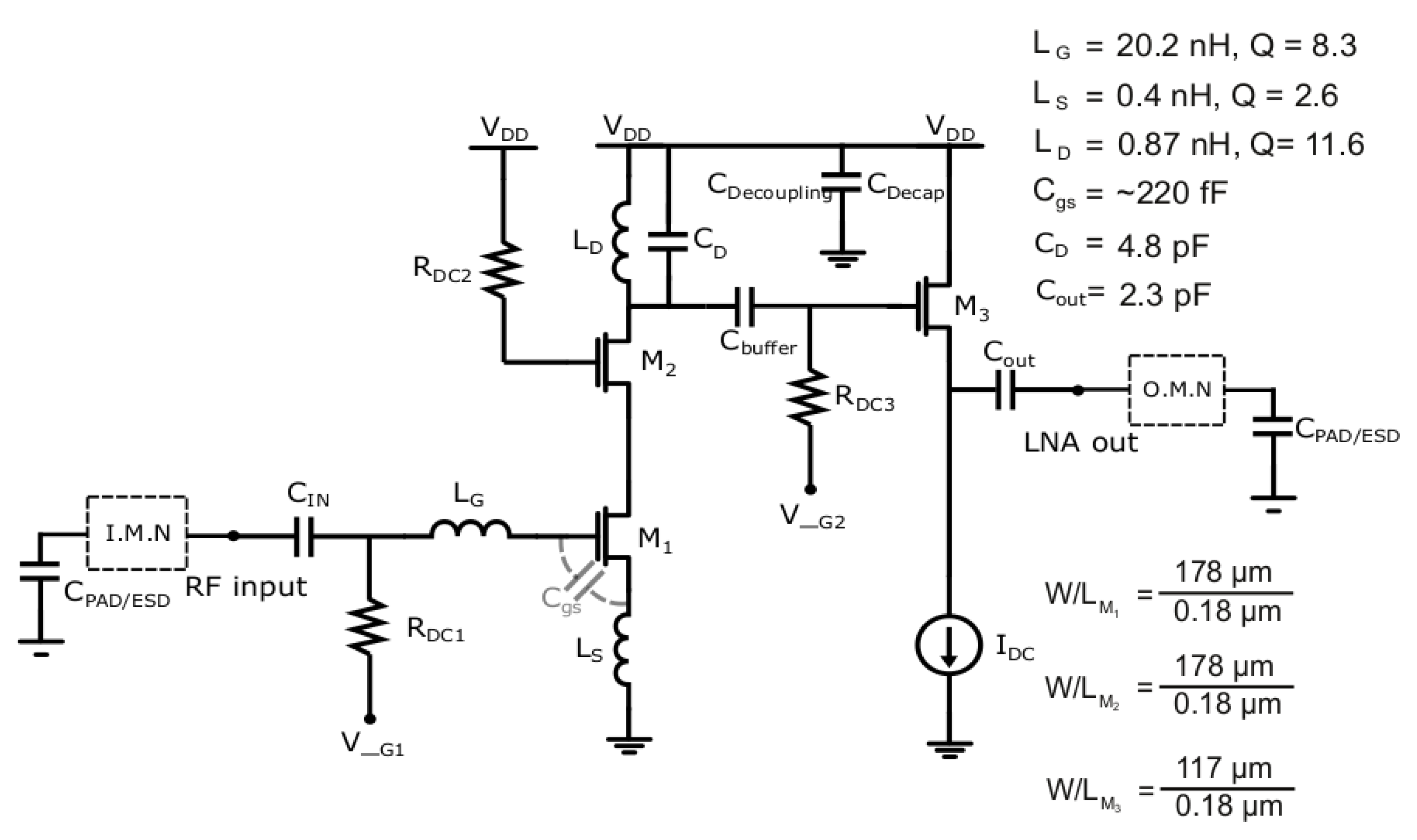
2.1. Circuit Topology

A cascode amplifier with inductive load and degeneration is appropriate for such a design goal and selected for evaluation in our work. Various different topologies can be applied for the implementation of LNAs, including common source [4,5], common gate [6,7], and cascode amplifiers [8,9]. In addition, resistive feedback [10] and noise-cancelling [11] LNAs are available options depending on the focus of design.
Our model focuses on low noise and high linearity with moderate gain, bandwidth, and power dissipation. The inherent characteristics of a cascode amplifier topology are beneficial in terms of gain, linearity, and bandwidth; hence, our work focus is in the cascode topology, in spite of the slightly higher noise figure due to the addition of one more transistor than common source and common gate structures. Figure 1 shows the circuit schematic of the cascode amplifier. The amplifier incorporates an inductive degeneration component L S , a gate inductor L G , and an output resonance inductor L D . L G and L S are designed for 50 Ω input impedance matching purpose. The input impedance of this circuit is equivalent to the equation below.
Z i n = s ( L g + L s ) + 1 s C g s + ( g m 1 C g s ) L s
The first and the second term of (1) are cancelled out at the operating frequency f 0 = 2.4 GHz and the real term ( g m / c g s ) L S matches to R S . Similarly the inductive load L D forms a LC tank with C g d of M2 and C d at the drain node of the cascode amplifier to resonate at the f 0 = 2.4 GHz. The buffer stage M3 is followed after the cascode amplifier stage for 50 Ω output impedance matching. The width of M1, M2 transistors usually match to accommodate the same amount of current through the transistors. The width determination process of W M 1 , W M 2 , and V o v is discussed in the following section. The noise figure is defined in (2).
N F = 1 + R g R s + γ α ( 1 + ω 2 c g s 2 ( R s + R g ) 2 ) 2
where K = u C o x W L , R g is gate resistance, R s is source resistance, γ / α is about 2/3 for long channel device and 2 for short channel device [12]. The second term represents gate induced noise from the gate resistance R g which can be minimized with efficient layout. With assumption that R s >> R g , the second term can be neglected. The third term describes the thermal noise from a MOSFET device. At a high frequency, ω 2 c g s 2 ( R s + R g ) 2 >> 1 since ω > ω t . The linearity IIP3 is difficult to be equated due to its complexity. Although there are multiple factors that affect IIP3 level, the biggest factor would be the nonlinear transconductance term g m 3 . Suppression of g m 3 can be key to improving IIP3. In short, it is barely possible to quantify IIP3 into a formula, hence it will be optimized by the gm/ID algorithm and the FoM combination.

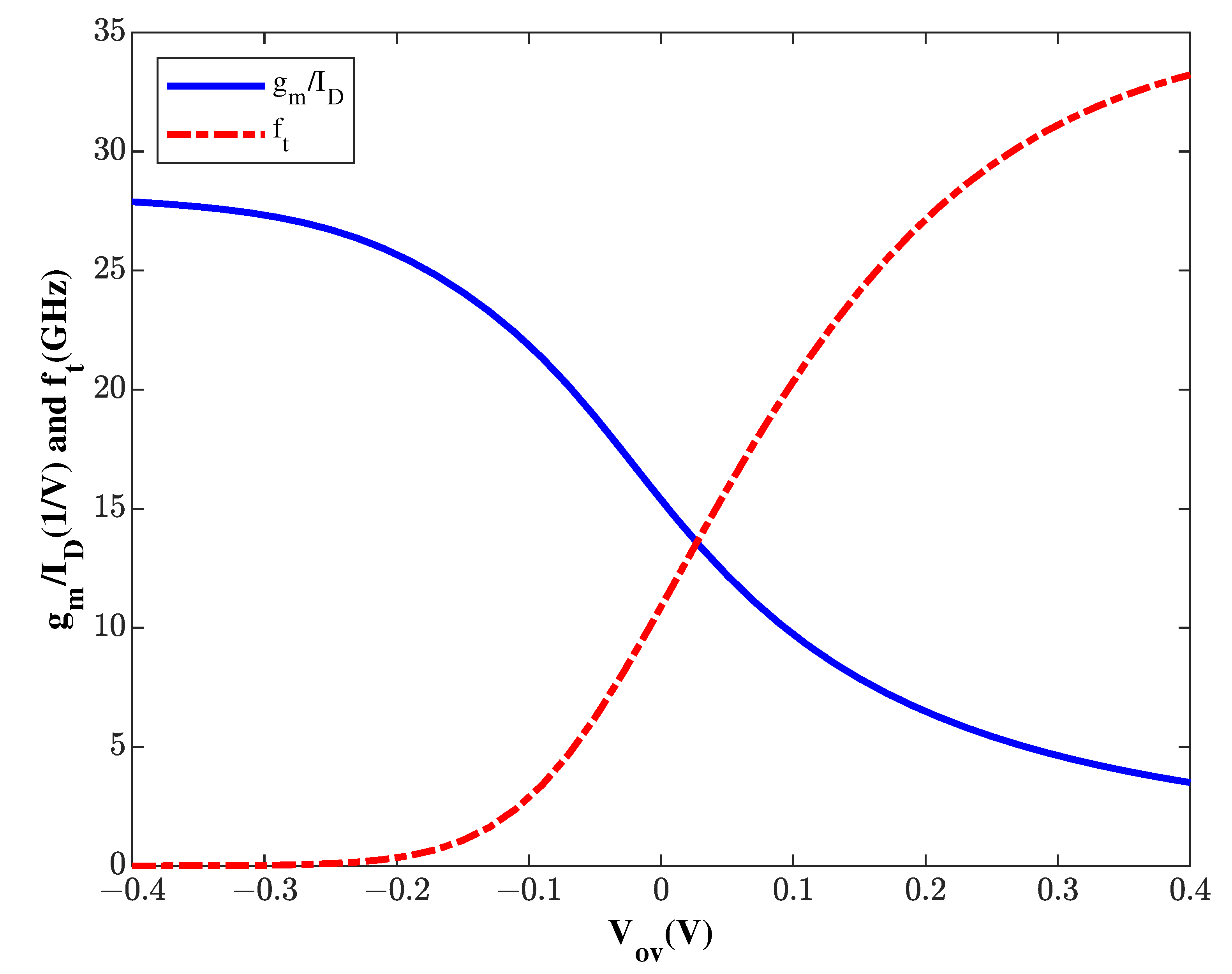
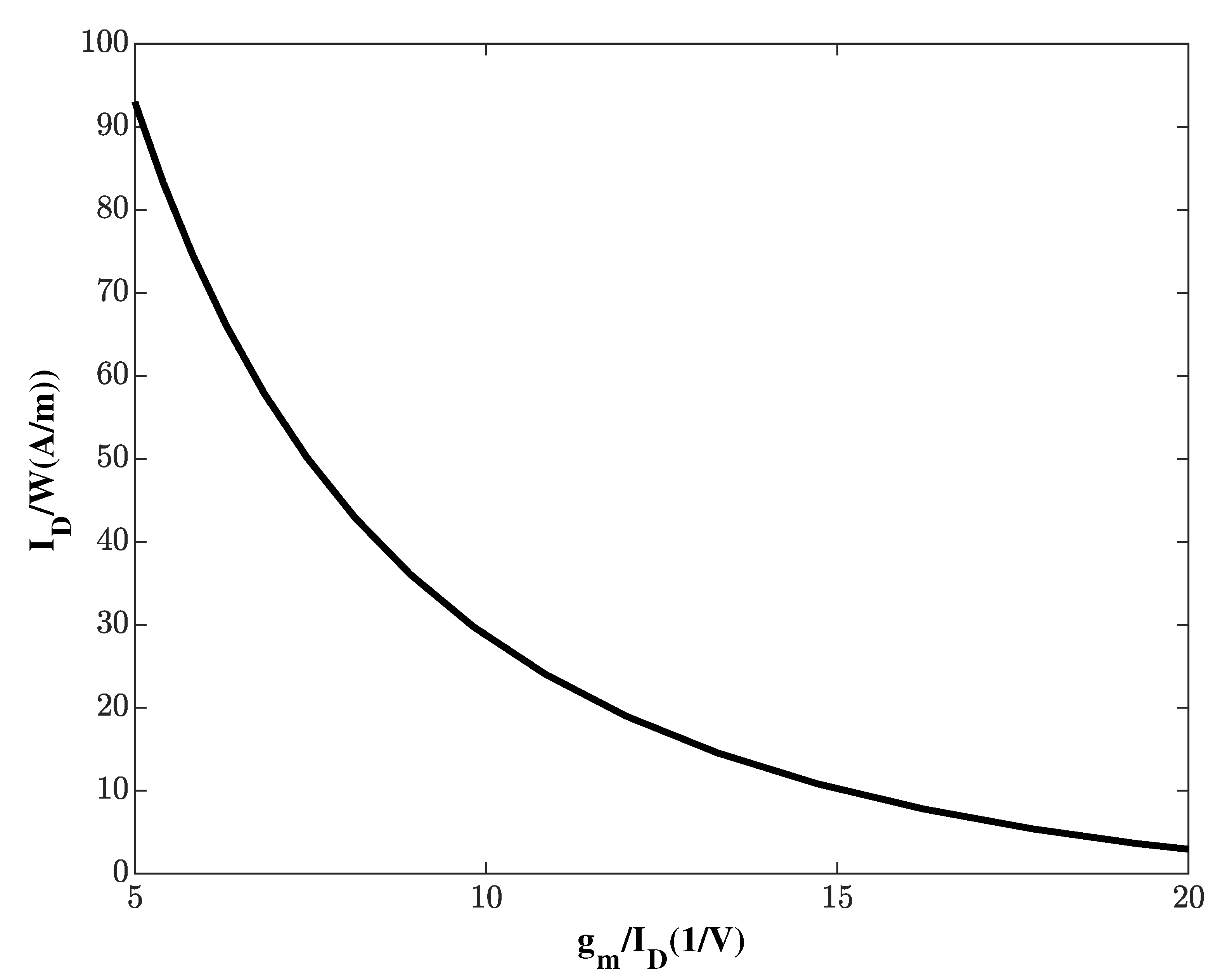
2.2. Parameters Determination Strategy

The g m / I D algorithm suggests a quantitative circuit design guidance for submicron MOSFET devices. To start the g m / I D based design, three reference charts need to be generated. These are: g m / I D vs. V o v and f t vs. V o v (Figure 2), I D / W vs. g m / I D (Figure 3) at V D S = 900 mV, L = 180 nm. g m / I D vs. V o v describes the transconductance efficiency w.r.t V o v which is equivalent to power efficiency. f t vs. V o v represents a unity current gain frequency w.r.t V o v that implies a capable maximum speed of MOSFETs. I D / W vs. g m / I D stands for the current density for unit width w.r.t transconductance efficiency serving as a reference to determine device width depending on the V o v and the current. A design flow for this LNA proceeds in the following steps:
  • Step 1. Set the power budget by setting current I D through the cascode amplifier.
  • Step 2. Determine the channel length.
  • Step 3. Vary V o v and find corresponding g m / I D points.
  • Step 4. Get I D / W for the g m / I D points from step 3.
  • Step 5. Compute width for the values in step 4.
  • Step 6. Run simulations on gain, noise figure, and linearity.
  • Step 7. Evaluate the FoM and finalize parameters.
The design optimization starts with fixing a power budget. A moderate power consumption is desired and was set to P d c = V D D × I D = 1.8 V × 5 mA = 9 mW. Thus, the current through the cascode amplifier is fixed to 5 mA based on this definition. The next step is to determine the channel length of M1 and M2. ω t , i.e., g m / c g s , is inversely proportional to L 2 and accordingly low ω t lessens intrinsic gain potential and escalates noise figure as described in (2). To obtain better performance in noise and speed, the channel length is set to the minimum length, L = 180 nm.
Then, V o v is adjusted to find an appropriate g m / I D for the design. The data chart (Figure 2) demonstrates the trend as V o v increases, g m / I D decreases while f t increases. In other words, when V o v is high (strong inversion), g m / I D is low and f t is high, while in weak inversion where V o v is low, g m / I D is high and f t is low. Next, the gain, noise, linearity, and power are evaluated, and, finally, the figure of merit FoM, is evaluated from (3) below:
F o M = S 21 × I I P 3 ( N F 1 ) × P D C
This FoM allows the designer to finalize the appropriate V o v and its corresponding W M 1 , W M 2 .

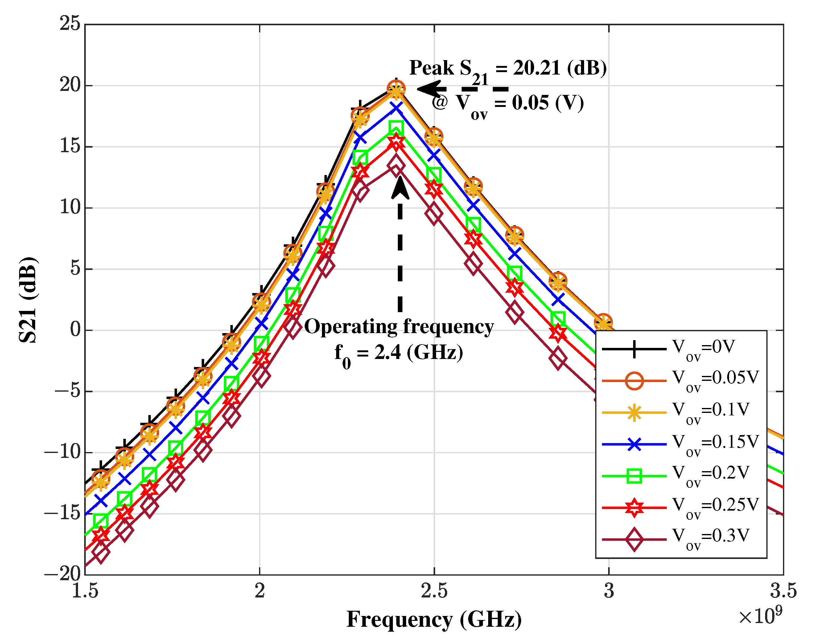
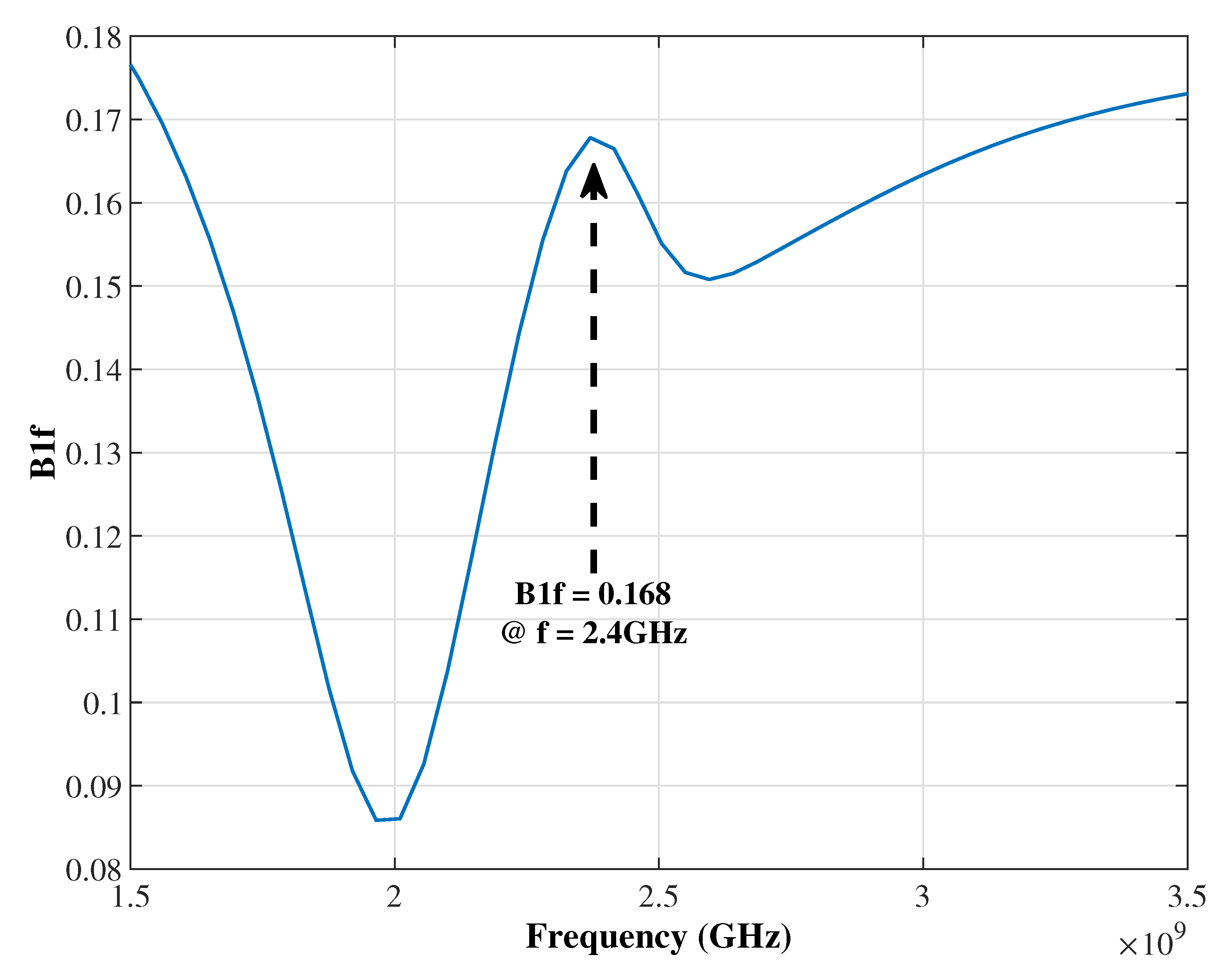
3. Simulation Results and Parameter Set-Up

To define the optimal bias point where noise, linearity, and gain level satisfy our targeted performance, simulations of S 21 , NF, and IIP3 are executed with the V o v values shown in Table 1, and the FoM is computed. By analyzing the results in Table 1, an optimal bias point is defined to be 0.1 V as detailed in Section 3.1 below.

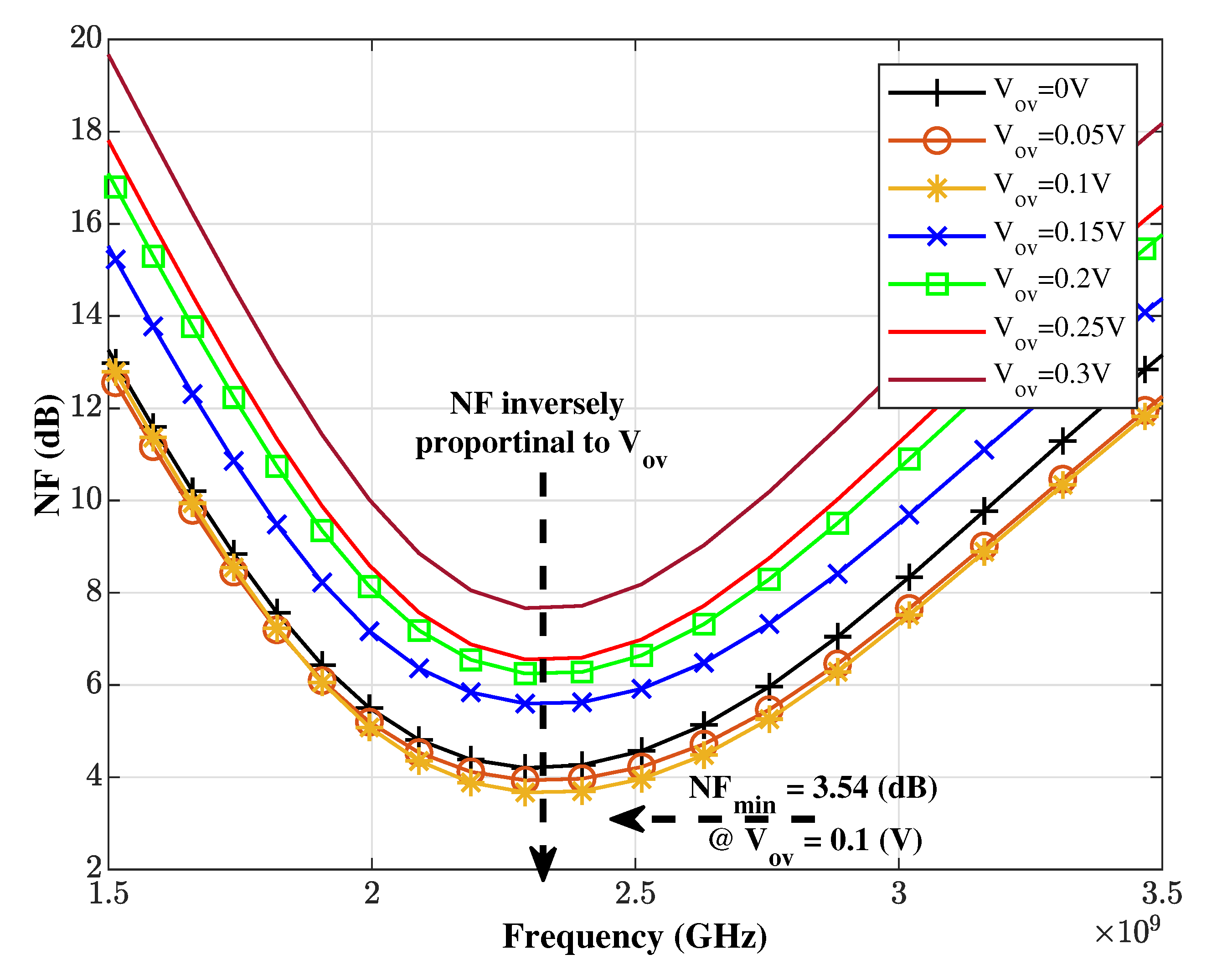
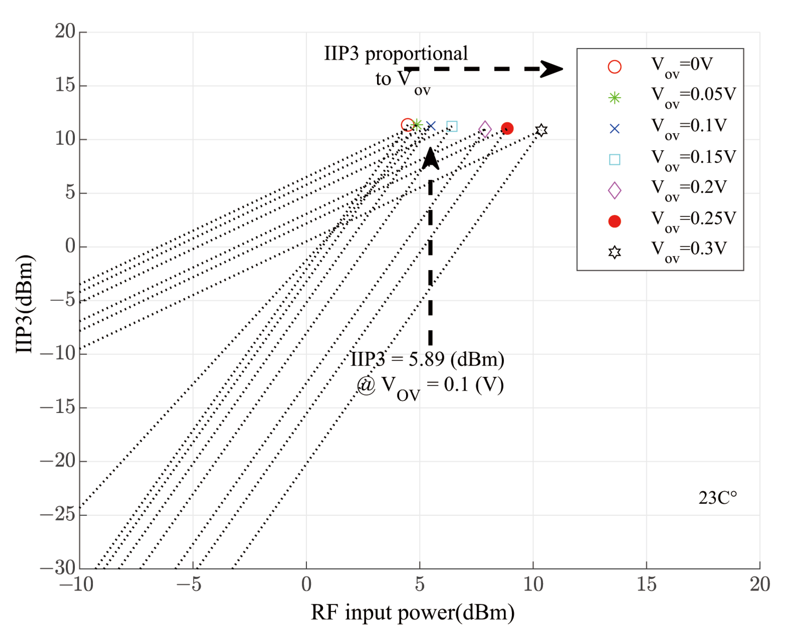
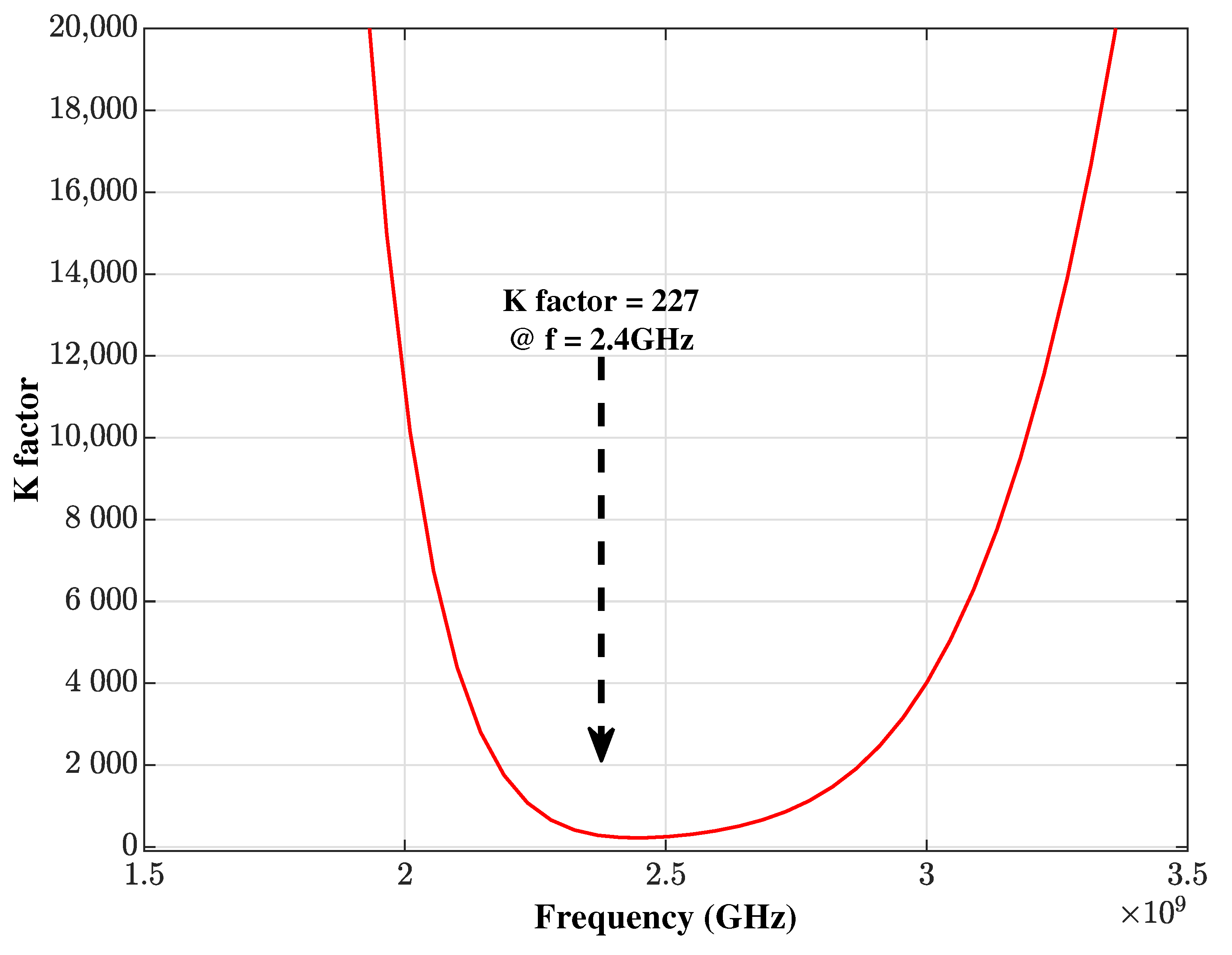
3.1. Simulation for Each V o v

The simulation is run on S 21 (Figure 4), NF (Figure 5) and IIP3 (Figure 6) for V o v from 0 to 0.3 V in 50 mV steps. Table 1 indicates that the FoM is inversely proportional to V o v providing strong insight for a parametric optimization except at V o v = 0 V. However, f t is too small at V o v = 0 V suggesting the realistic bias point is V o v above 0.05 V. Additionally, the device width for each V o v is computed from the I D / W chart (Figure 3) and Table 1. P D C is 9 mW for all cases.
Inspecting the results, we see that the best S 21 and NF response is at V o v = 0.05 V while IIP3 improves as V o v increases. The results verified that the optimal gain and noise occurs at moderate inversion, while the linearity showed better response in the strong inversion layer domain. Hence, the optimal bias point for this application is in a moderate inversion domain corresponding to V o v = 0.1 V, resulting in low noise, high linearity, and moderate gain.

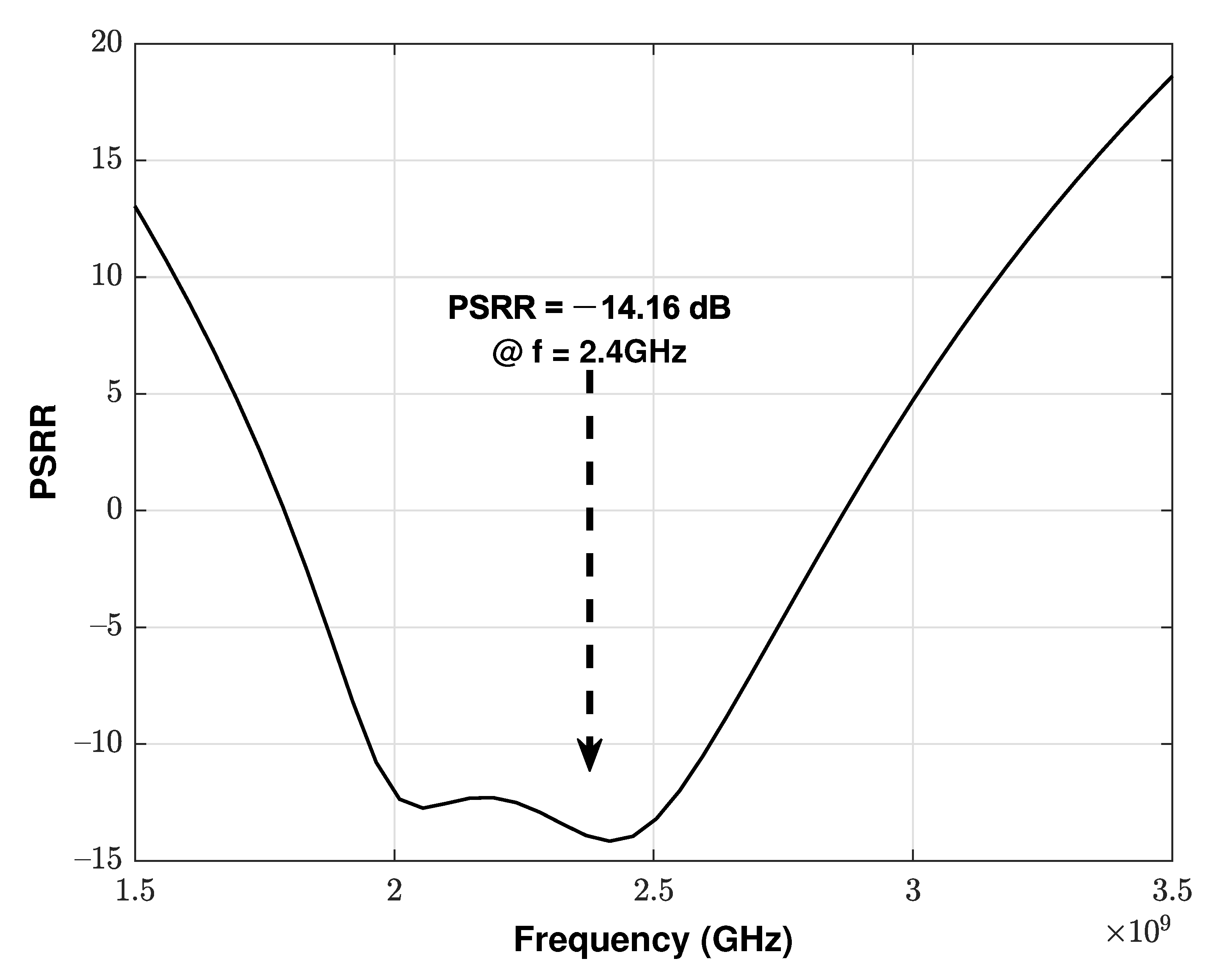
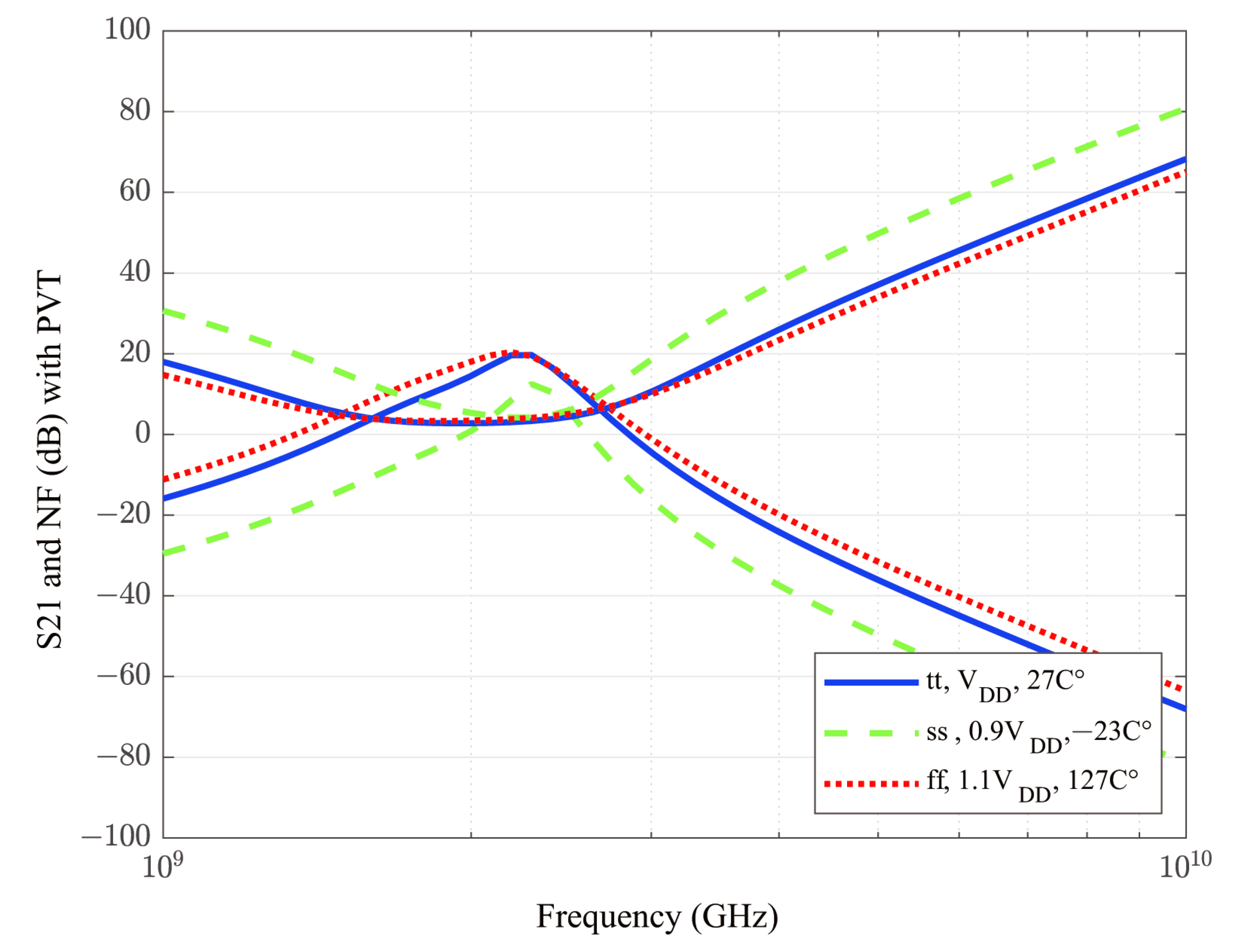
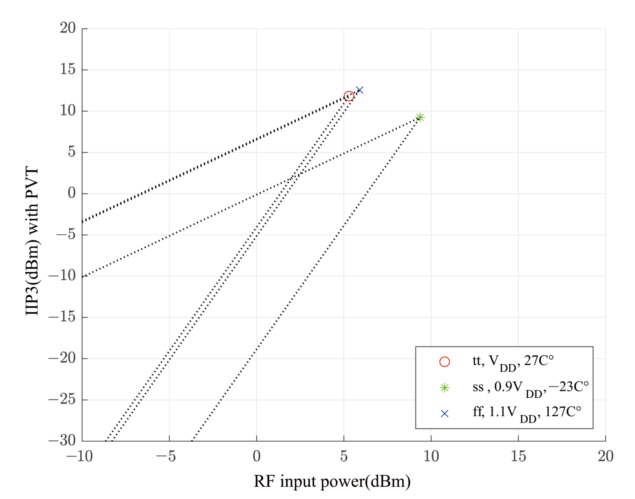
3.2. Optimized Parameters and Reliability Simulations

Thus, for optimal bias point V o v = 0.1 V, the reference data (Figure 2) and (Figure 3) indicate that g m / I D = 10 (m/V), f t = 20 (GHz), I D / W = 28 (A/m) for a device width W M 1 , W M 2 is 178 μ m (Table 1), and for these optimized parameters, S 21 = 19.91 dB, NF = 3.54 dB, and IIP3 = 5.89 dBm.
Several reliability tests were also carried out, which are: stability, PSRR and PVT simulations. First, stability simulation was performed by validating the K factor and the Δ factor(=B1f) which are equal to
K = 1 | S 11 | 2 | S 22 | 2 + | D | 2 2 | S 22 | | S 12 |
Δ = 1 + | S 11 | 2 | S 22 | 2 | D | 2
where D = | S 11 S 22 S 21 S 12 | . Unconditional stability is secured when both K > 1 and Δ > 0 conditions are satisfied by ensuring no oscillation at any frequency domain. Figure 7 and Figure 8 showed K = 227 and Δ = 0.168, demonstrating the unconditional stability of this LNA. Next is the power supply rejection ratio (PSRR). PSRR represents vulnerability of a system output against power supply noise injection. The lower the PSRR, the more reliable it is against the power supply noise injection. Our result in Figure 9 showed PSRR = −14.16 dB, proving the supply noise reliability of this circuit design. Lastly, process, voltage, and temperature (PVT) variation simulations were performed. A process variation is inevitable within the process of semiconductor fabrication. We used three corners: t t (typical), f f (fast), and s s (slow) in these simulations. A temperature variation is another inevitable factor in real application. The tests were executed at 27 °C, −23 °C, and 127 °C to demonstrate the circuit operation at any extreme temperature. A voltage variation is a simulation against supply voltage variation where V D D was swept for V D D , 0.9 V D D and 1.1 V D D to encounter ±10% variation. In summary, simulations were carried out at three conditions:
  • t t (typical-typical), V D D , 27 °C
  • s s (slow-slow), 0.9 V D D , −23 °C
  • f f (fast-fast), V D D , 127 °C
to reflect the worst case scenarios. Figure 10 summarizes the PVT simulation results for S 21 and NF and Figure 11 indicates the PVT result for IIP3. The worst case results were S 21 = 12.4 dB (at condition 2), NF = 3.56 dB (at condition 2), and IIP3 = 5.89 dBm (at condition 1).
The circuit layout is shown in Figure 12 which was designed for the area of approximately 500 μ m × 530 μ m. The center part shows the core cascode RF NMOS transistors.
The transistor dimension (located at the center of the layout) is 17 μ m × 19 μ m which is less than 0.2% of the total area of the LNA. The top left is the drain inductor L D , and the source inductor L S is at the bottom left. The gate inductor L G is located at the bottom right. The drain load capacitor C D , the input and output capacitors C i n and C o u t and the AC coupling C b u f f e r are shown on the upper right corner. Our simulation results reflected parasitic effects through PEX extraction and the vender provided inductor synthesis tool for EM effect analysis. The circuit is designed based on 180 nm with 1P6M + UTM metal option. All the simulations are performed by Spectre through Cadence ADE tool.
As shown in Table 2 below, the performance of this LNA compares well to performance to previous works [13,14,15,16,17,18,19]. Aneja’s report utilized the dual band load technique which showed great performance in terms of S 21 , however its power consumption was excessively high compared to most applications. Park’s LNA which included a poly-phase filter revealed excellent power efficiency. However, noise was relatively not satisfactory and linearity was significantly limited. Luo came up with a reconfigurable active inductor for an LNA and proved great S 21 and NF performance, but at the cost of high power consumption. Liu and Bozorg’s works applied the active feed-forward technique and noise reduction technique, respectively. In both works, they showed decent gain and noise responses, however, linearity were limited. Chang’s work used a body floating and self-bias technique. It demonstrated excellent power efficiency though gain and its linearity response was not as competitive compared to other works. Finally, Gao’s report represented a frequency-selective gain equalization technique in an effort to secure superior gain response. However, the relatively low linearity and high power consumption was not practical. The analysis of previous works compared to our own work proves our excellent results in terms of overall performance which includes S 21 , NF, IIP3, P d c , and demonstrated superiority of our g m / I D and FoM combined design methodology.

4. Conclusions

The modeling and evaluation of an LNA is carried out by combining the g m / I D algorithm and the FoM index method. The device is based on 180 nm CMOS technology and operates at f 0 = 2.4 GHz. Design parameters were determined using g m / I D vs. V o v , f t vs. V o v , and I D / W vs. V o v data charts (Figure 2 and Figure 3) and computing the FoM to demonstrate an optimal bias point. The results revealed that optimal values for S 21 and noise figure were obtained at V o v = 0.1 V (Table 1) where great linearity is obtained without any significant degredation in the S 21 parameter and noise. A comparison of this LNA and previous works in Table 2 shows high linearity and power efficiency with comparble S 21 and NF. The figure of merit was computed to guide the parametric optimization. The optimized model showed S 21 = 19.91 dB, NF = 3.54 dB, I I P 3 = 5.89 dBm, P D C = 9 mW, verifying the effectiveness of characterization capabilities of the g m / I D algorithm process and the FoM index method combined.

Author Contributions

Conceptualization, J.C.; methodology, J.C.; validation, J.C. and A.A.I.; investigation, J.C.; writing—original draft preparation, J.C.; writing—review and editing, J.C. and A.A.I.; visualization, J.C.; supervision, A.A.I.; project administration, A.A.I. All authors have read and agreed to the published version of the manuscript.

Funding

This research received no external funding.

Data Availability Statement

Not appliable.

Conflicts of Interest

The authors declare no conflict of interest.

References

  1. Iliadis, A.; Kim, K. Theoretical foundation for upsets in CMOS circuits due to high-power electromagnetic interference. IEEE Trans. Device Mater. Reliab. 2010, 10, 347–352. [Google Scholar] [CrossRef]
  2. Pinjare, S.; Nithya, G.; Nagaraja, V.; Sthuthi, A. A Gm/Id Based Methodology for Designing Common Source Amplifier. In Proceedings of the 2018 2nd International Conference on Micro-Electronics and Telecommunication Engineering (ICMETE), Ghaziabad, India, 20–21 September 2018. [Google Scholar]
  3. Chung, J.; Iliadis, A. Modeling a High Linearity, Low Noise Gilbert Cell Mixer using Three Optimization Techniques. In Proceedings of the 2020 IEEE 63rd International Midwest Symposium On Circuits And Systems (MWSCAS), Springfield, MA, USA, 9–12 August 2020; pp. 790–793. [Google Scholar]
  4. Balodi, D.; Verma, A.; Govidacharyulu, P. A high gain low noise amplifier design & comparative analysis with other MOS-topologies for Bluetooth applications at 130nm CMOS. In Proceedings of the 2016 IEEE Industrial Electronics and Applications Conference (IEACon), Kota Kinabalu, Malaysia, 20–22 November 2016; pp. 378–383. [Google Scholar]
  5. Chung, J.; Iliadis, A. Design and optimization of a CMOS IC novel RF tracking sensor. Int. J. Circuit Theory Appl. 2021, 49, 801–819. [Google Scholar] [CrossRef]
  6. Arshad, S.; Ramzan, R.; Qamar-ul-Wahab. Wideband common gate LNA with novel input matching technique. In Proceedings of the 2016 5th International Conference on Modern Circuits and Systems Technologies (MOCAST), Thessaloniki, Greece, 12–14 May 2016. [Google Scholar]
  7. Shim, Y.; Kim, C.; Lee, J.; Lee, S. Design of full band UWB common-gate LNA. IEEE Microw. Wirel. Compon. Lett. 2007, 17, 721–723. [Google Scholar] [CrossRef]
  8. Eshghabadi, F.; Banitorfian, F.; Noh, N.; Mustaffa, M.; Abd Manaf, A. Fully-hybrid computer-aided RF LNA design and evaluation for GSM-1900 standard band. In Proceedings of the 2015 6th Asia Symposium On Quality Electronic Design (ASQED), Kula Lumpur, Malaysia, 4–5 August 2015; pp. 177–180. [Google Scholar]
  9. Chen, Y.-C.; Kuo, C.-N. A 6-10-GHz ultra-wideband tunable LNA. Proc. IEEE Int. Symp. Circuits Syst. 2005, 5, 5099–5102. [Google Scholar]
  10. Lin, Y.; Wang, C.; Lee, G.; Chen, C. High-Performance Wideband Low-Noise Amplifier Using Enhanced π-Match Input Network. IEEE Microw. Wirel. Components Lett. 2014, 24, 200–202. [Google Scholar] [CrossRef]
  11. Jussila, J.; Sivonen, P. A 1.2-V Highly Linear Balanced Noise-Cancelling LNA in 0.13-μm CMOS. IEEE J. Solid-State Circuits 2008, 43, 579–587. [Google Scholar] [CrossRef]
  12. Li, X. Low Noise Design Techniques for Radio Frequency Integrated Circuits. Bachelor’s Thesis, University of Washington, Seattle, WA, USA, 2004. [Google Scholar]
  13. Aneja, A.; Li, X.; Chong, P. Design and analysis of a 1.1 and 2.4 GHz concurrent dual-band low noise amplifier for multiband radios. AEU Int. J. Electron. Commun. 2021, 134, 153654. [Google Scholar] [CrossRef]
  14. Park, B.; Kwon, K. 2.4-GHz Bluetooth low energy receiver employing new quadrature low-noise amplifier for low-power low-voltage IoT applications. IEEE Trans. Microw. Theory Tech. 2021, 69, 1887–1895. [Google Scholar] [CrossRef]
  15. Luo, Y.; Xia, T. Design of Reconfigurable Low Noise Amplifier Based on Active Inductor. In Proceedings of the 2020 IEEE International Conference on Artificial Intelligence and Computer Applications (ICAICA), Dalian, China, 27–29 June 2020. [Google Scholar]
  16. Liu, Z.; Boon, C.; Yu, X.; Li, C.; Yang, K.; Liang, Y. A 0.061-mm2 1–11-GHz Noise-Canceling Low-Noise Amplifier Employing Active Feedforward With Simultaneous Current and Noise Reduction. IEEE Trans. Microw. Theory Tech.. 2021, 69, 3093–3106. [Google Scholar] [CrossRef]
  17. Bozorg, A.; Staszewski, R. A 0.02–4.5-GHz LN(T)A in 28-nm CMOS for 5G exploiting noise reduction and current reuse. IEEE J. Solid-State Circuits 2021, 56, 404–415. [Google Scholar] [CrossRef]
  18. Chang, J.; Lin, Y. 3–9-GHz CMOS LNA using body floating and self-bias technique for sub-6-GHz 5G communications. IEEE Microw. Wirel. Components Lett. 2021, 31, 608–611. [Google Scholar] [CrossRef]
  19. Gao, H.; Li, N.; Li, M.; Wang, S.; Zhang, Z.; Kuan, Y.; Yu, X.; Gu, Q.; Xu, Z. A 6.5–12 GHz balanced variable gain low-noise amplifier with frequency-selective non-foster gain equalization technique. In Proceedings of the 2020 IEEE/MTT-S International Microwave Symposium (IMS), Los Angeles, CA, USA, 4–6 August 2020. [Google Scholar]
Figure 1. The schematic of cascode amplifier circuit.
Electronics 11 00976 g001
Figure 2. g m / I D , f t vs. V o v data chart.
Electronics 11 00976 g002
Figure 3. I D / W vs. g m / I D data chart.
Electronics 11 00976 g003
Figure 4. S 21 vs. frequency.
Electronics 11 00976 g004
Figure 5. Noise Figure vs. frequency.
Electronics 11 00976 g005
Figure 6. Third-order intercept point vs. V o v .
Electronics 11 00976 g006
Figure 7. K factor vs. frequency for Stability test.
Electronics 11 00976 g007
Figure 8. B1f vs. frequency for Stability test.
Electronics 11 00976 g008
Figure 9. PSRR vs. frequency.
Electronics 11 00976 g009
Figure 10. S21 and NF (dB) with PVT vs. frequency.
Electronics 11 00976 g010
Figure 11. Third-order intercept point with PVT vs. V o v .
Electronics 11 00976 g011
Figure 12. The layout of the designed LNA with the area of 500 μ m × 530 μ m.
Electronics 11 00976 g012
Table 1. The LNA parameters according to V o v .
V ov (V) g m / I D (1/V) f t (GHz) S 21 (dB)IIP3 (dBm)NF (dB)W ( μ m)FoM
025.62.819.724.474.15883.16
0.0512.21120.214.873.982953.67
0.11015.819.915.893.541783.62
0.157.92018.626.525.621172.92
0.26.524.116.67.96.2842.8
0.255.42715.38.966.45652.79
0.34.63113.2110.217.89742.17
Table 2. A comparison table of the LNA and other works.
Reference S 21
(dB)
NF
(dB)
IIP3
(dBm)
Power
(mW)
f c
(GHz)
Supply
Voltage (V)
Area
( mm 2 )
CMOS
Tech (nm)
This work19.913.545.8992.41.80.26180
Aneja [13]20.134.91082.43N/AMIC
Park [14]49.58.2−25.752.162.40.81.1665
Luo [15]192.65N/A20.12.41.80.023180
Liu [16]14–173.5–5.5−2.891–111.20.06140
Bozorg [17]15.22.09–3.2−4.6–3.54.50.02–4.510.0328
Chang [18]7.5–10.73.41−6.23.32.4–9.110.74180
Gao [19]20.73.26−12756.5–121.30.9855
Publisher’s Note: MDPI stays neutral with regard to jurisdictional claims in published maps and institutional affiliations.

