2. Basic Information
A Mealy FSM logic circuit can be represented by two systems of Boolean functions (SBFs) [
14]. One of these SBFs represents FSM outputs connected with operational units of a particular digital system. The second SBF represents input memory functions (IMFs). The arguments of these SBFs are external FSM inputs and internal state variables. The inputs form a set
; the IMFs create a set
. An FSM circuit is represented by the following SBFs:
The state variables
encode internal states from a set
. To encode M states, the minimum number of state variables is determined as [
1]
Each state
is represented by a binary code
having
R bits. These codes are kept into the state code register (RG). In this article, we discuss a case when the RG has informational inputs of D type. This is the most common case [
15]. The systems (
1) and (
2) determine so called
P Mealy FSM [
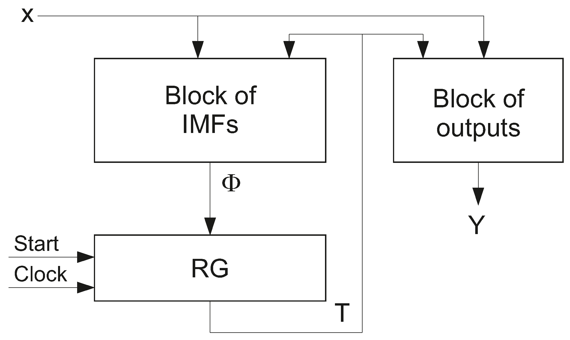
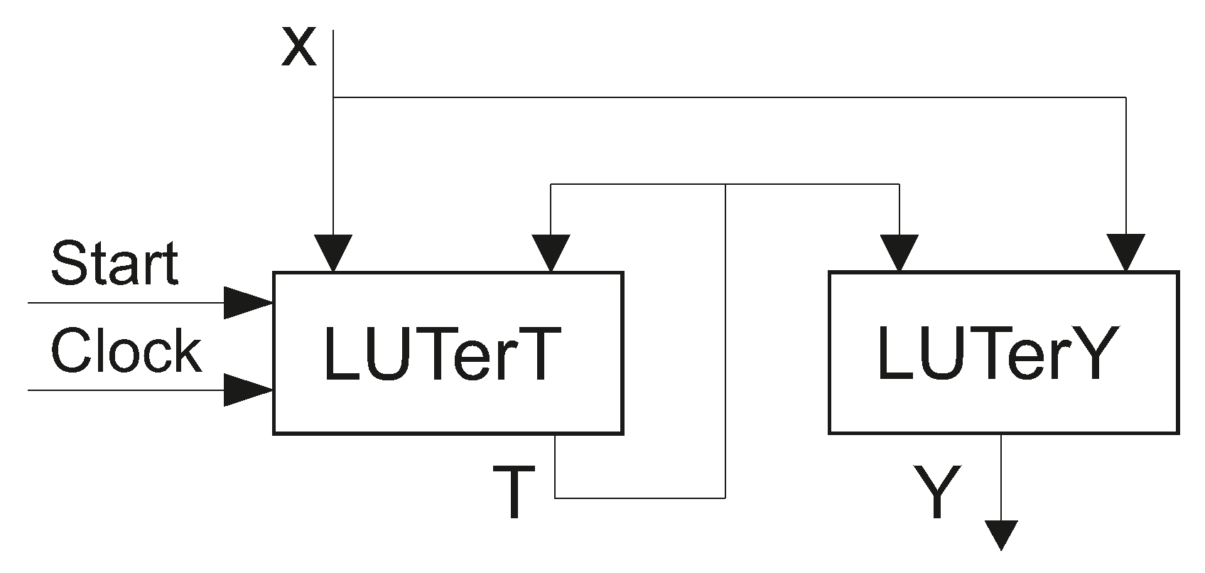
2] shown in
Figure 1.
In
Figure 1, the block of IMFs is implemented using SBF (
2); the block of outputs is based on SBF (
1). The state register has
R D flip-flops. The
r-th flip-flop keeps the state variable
. The pulse
allows clearing the content of RG. This pulse loads a code of the initial state
into RG. As a rule, the code
consists of zeros. The pulse
shows an instant when the RG content can be changed by current IMFs.
As a rule, an FSM is represented by either a state transition table (STT) [
1] or a state transition graph (STG) [
5]. To obtain the systems (
1) and (
2), it is necessary to form an FSM direct structure table (DST) [
14]. In this article, we start from the STG. Next, this graph is transformed into the equivalent STT. Using the STT, we construct the DST.
An STG is a directed graph whose nodes correspond to FSM states. Interstate transitions are represented by edges of STG. Each edge is marked by a combination of inputs causing a particular transition and collection of outputs (COs) generated during this transition. An STT is a representation of STG as a list of interstate transitions. An STT includes five columns with: a current state
; a state of transition
; an input signal
which is a conjunction of some inputs (or their complements) determining this particular transition; CO
generated during this transition;
h is a number of transition (
) [
1].
A DST includes the columns with state codes and IMFs [
14]. These columns are: the code of the current state
, the code of the next state
, and a collection of IMFs
equal to 1 to load the code of the next state into the state register RG.
In this paper, we consider a case when internal resources of FPGA chips are used for implementing SBFs (
1) and (
2). An FSM circuit is implemented using configurable logic blocks (CLB) of FPGAs produced by Xilinx [
10]. A circuit is represented as a network of CLBs connected with help of a programmable routing matrix [
16]. In this paper, we discuss a case when CLBs include LUTs, multiplexers, and programmable flip-flops. Using the notation [
17], we denote as
-LUT a single-output LUT with
inputs. If a Boolean function depends on up to
arguments, then it is represented by a single-LUT logic circuit. If the number of LUT inputs is less than the number of arguments, then a circuit has more than a single level of LUTs. To implement multi-level circuits, the methods of functional decomposition (FD) are used [
18,
19]. As a rule, the FD-based circuits have the complicated systems of “spaghetti-type” interconnections [
2].
We discuss a case when each CLB is a part of slice [
10]. The slice includes internal multiplexers. They can be used for changing the number of LUT inputs within one slice. The internal multiplexers are connected with LUTs by a system of fast inter-slice interconnections. Due to this, the delay time for 6-, 7-, and 8-input LUTs is practically the same for SLICEL of Virtex-7 [
20,
21]. This approach makes it possible to flexibly adapt the LUT parameters to the characteristics of the function being implemented. For example, the SLICEL of Virtex-7 includes four 6-LUTs, 8 flip-flops, and 27 multiplexers [
20]. Each 6-LUT can be used as two 5-LUTs with shared inputs. This explains the presence of eight flip-flops in each SLICEL. Using internal multiplexers allows combining two 6-LUTs into a single 7-LUT. Next, four 6-LUTs can be combined into a single 8-LUT. The control inputs of multiplexers can be used as inputs of 7- and 8-LUTs. Each SLICEL possesses special carry chains used for organization of fast multi-bit adders. It is worth noting that these circuits can be used to implement arbitrary logic circuits [
22,
23].
In this paper, we use multiplexers to generate functions (
1) and (
2). We denote a multiplexer having
K data inputs as
. Using a single 6-LUT, we can implement a circuit of
. It has two control inputs and four data inputs. Further, we can organize an
with the help of two 6-LUTs. Its circuit has only slightly bigger delay than a circuit of a
[
20]. It is possible due to using fast interconnections inside a slice. If a
has the control inputs
, then its circuit includes four 6-LUTs controlled by
. To implement a
, two slices and inter-slice interconnections are used. As a result, a
is much slower than a
.
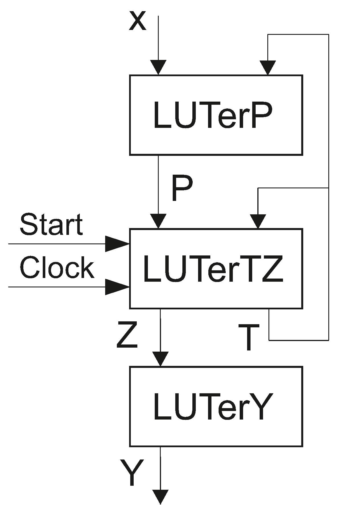
In LUT-based FSMs, the flip-flops of RG are distributed among LUTs generating functions (
1). Due to this, the RG is “hidden” inside the slices where the IMFs are generated. There are two blocks in an LUT-based
P Mealy FSM (
Figure 2).
In this paper, we denote as LUTer a logic block consisting of LUT-based CLBs. In the
P Mealy FSM (
Figure 2), a
implements SBF (
1) and
implements SBF (
2). To control the RG, the pulses
and
are used.
If each function from systems (
1) and (
2) depends on not more than
arguments, then both blocks of LUT-based
P Mealy FSM (
Figure 2) are represented by single-level circuits. For Xilinx-based solutions, an LUT has 6 inputs [
10]. There is no point in increasing this value, because
provides the best balance for such LUT characteristics as the occupied chip area, performance and consumed power [
16]; however, even for FSMs with average complexity [
14], it could be up to 40 arguments in functions (
1) and (
2). Obviously, there is a distinct imbalance between such big number of arguments in SBFs representing FSM circuits and a fairly small value of LUT inputs. This imbalance requires improving synthesis methods of LUT-based FSMs.
Denote as
the number of literals in a sum-of-product of function
. If the condition
holds, then it is impossible to represent the function
by a single-level circuit. In this case, it is very important to optimize the system of connections between different slices of an FSM circuit. This follows from the fact that more than 70% of the power consumption is due to the interconnections [
2]. Moreover, time delays of the interconnection system are starting to play a major role in comparison with CLB delays [
18]. The results of research [
2] show that the optimization of interconnections leads to increasing the maximum operating frequency and reducing the power consumption of LUT-based FSM circuits. This can be performed, for example, using various methods of structural decomposition [
2].
3. Related Work
There are a huge number of methods for improving characteristics of circuits targeting LUT-based FSMs. The survey of these methods can be found, for example, in [
2,
12]. These methods should be applied if the condition (
4) holds [
2]. These methods can improve either the LUT count or the maximum operating frequency or the power consumption [
24]. Sometimes, these methods are looking for a solution that allows joint improvement of more than only one FSM circuit’s characteristic. In this paper, we propose a method for decreasing the number of LUTs (this is an LUT count) of FPGA-based Mealy FSMs.
This task can be solved using various methods of state assignment [
25,
26,
27]. In these methods, the number of bits in the state codes ranges from the minimum determined by formula (
3) to the maximum determined by the total number of states,
M. If
, then this is a one-hot state assignment. These approaches are used in both academic and industrial CAD tools. The examples of academic systems are SIS [
28] and ABC by Berkeley [
29,
30]. The examples of industrial systems are Vivado [
31] of Xilinx and Quartus of Intel (Altera) [
32].
Now, there is no single universal method of state encoding that provides the best possible characteristics of FSM circuits. The applicability of a particular method can be judged both by the required number of state variables (
R) and by the number of FSM inputs (
L). As follows from [
33], the one-hot codes improve FSM characteristics if
. The rather small value of
increases the influence of the value of
L on the characteristics of LUT-based FSM circuits [
2]. It is shown in [
34] that it is better to use the codes with the minimum number of bits (
), if
.
So, in one case, it is better to use the one-hot state codes, and, in the other case, it is better to use the maximum binary state assignment with
; therefore, it makes sense to compare several state assignment methods for the same FSM and find a method with the best characteristics. Due to this, we have compared the FSMs circuits produced by our proposed approach with FSM circuits produced by four other methods of state assignment. As a base for comparison, we use: the method of maximum state assignment Auto used in the CAD tool Vivado [
31] by Xilinx; one-hot state assignment used in Vivado; the algorithm JEDI [
28] which is one of the best methods of binary state assignment [
19]. Our choice of Vivado is dictated by the fact that it operates with FPGAs of Xilinx. Further, we compared FSM circuits produced by our approach with three-block FSM circuits [
11].
In this paper, we propose a method leading to four-block FSM circuits. It belongs to the methods of structural decomposition (SD) [
2]. The main idea of these methods is the elimination of the direct connection between FSM outputs
and IMFs
, on the one hand, and FSM inputs
and state variables
, on the other hand. The SD leads to an increase in the total number of implemented functions having significantly fewer arguments than functions (
1) and (
2). These methods are analyzed, for example, in [
2].
In [
11], we have proposed an optimization method based on the combined use of two structural decomposition methods. These methods are the replacement of FSM inputs and encoding of collections of outputs. This approach leads to so called
Mealy FSMs. Let us discus these two methods.
The first method is based on the replacement of inputs
by additional variables
, where
. The method uses the fact that transitions from any state
depend on
inputs, where
[
14]. In the case of LUT-based FSMs, the variables
are generated by an additional block
. This block implements the system
The second method is based on the fact that only a limited set of outputs is formed during transitions from any FSM state. Each transition is accompanied by generating some CO
, where
. Each CO
is encoded by a binary code
having
bits, where
To encode these COs, additional variables
are used.
In
FSMs, a special block
generate FSM outputs as functions
The variables
and IMFs are generated by a block
:
So, the structural diagram of an LUT-based
Mealy FSM includes three blocks connected in series (
Figure 3).
There is a hidden register RG inside the block . This explains why pulses and enter the block . Obviously, the informational inputs of D flip-flops are connected with IMFs .
As shown in [
11], such joint usage of two methods of SD leads to a significant decrease in the LUT count compared with other investigated methods; however, the gain in LUTs is significantly reduced if the condition (
4) is met for the functions
, where these systems are represented as (
8) and (
9). In this case, the circuit of
is designed using the methods of functional decomposition [
13]. As a result, there are several levels of LUTs in the circuit of
with all the negative consequences.
The proposed method is an evolution of methods of twofold state assignment [
17]. These methods are based on construction a partition
of the set of states by the classes of compatible states:
. Each state
determines a set
including FSM inputs causing transitions from this state. Inside each class, the states are encoded using maximum binary codes. If a set
includes
elements, then it is enough
variables to encode these states by maximum binary codes. One additional code corresponds to the relation
.
We use the same definition of compatible states as the one propose in the paper [
17]. The states
are compatible if
In (
11), the symbol
stands for the number of inputs determining transitions from states
. These inputs form a set of inputs
.
To create the partition
with minimum number of classes,
J, we use the method from [
17]. Each class
consists of compatible states. Each class
determines local sets of inputs
and outputs
. If outputs
are generated during transitions from states
, then they are included into a set
.
In the case of twofold state assignment, each state
has two codes [
17]. The code
determines the state
as an element of the set
A. The extended state code (ESC) [
35]
determines this very state an element of a compatibility class
. Each class
determines a collection of partial functions generating by a block
. These partial functions are partial outputs
and partial IMFs
. The set
includes IMFs generating during the transitions from the states
. These partial functions are denoted as
and
. Because of (
11), each partial function is represented by a single LUT.
An ESC consists of J fields. The j-th field has bits and corresponds to the class . So, there are bits in ESCs. If the relation holds, then only bits from the j-th field differ from zeros.
In [
17], it is propose to produce ESCs by the transforming state codes
kept into RG. Unfortunately, the transformation requires an additional block of CLBs which consumes some internal resources of a chip and decreases the performance of a resulting FSM circuit. The improvement of this approach is proposed in [
35]. In this case, the codes
are generated in parallel with FSM outputs. This approach allows eliminating the block of code transformation; however, this approach also has some drawbacks. Firstly, there are
flip-flops in the RG. Secondly, the total number of LUTs generating IMFs is increased by
compared to the previous approach.
The experiments [
35] show that using only ESCs allows increasing performance up to 15.9% compared with equivalent FSMs based on the twofold state assignment. The growth of operating frequency is accompanied by a slight growth in the LUT count (up to 7.7%). In this paper, we propose a method of reducing the LUT count in
Mealy FSM. The method is based on the replacing ESCs by complex state codes proposed in this paper.
4. Main Idea of the Proposed Method
The proposed method is based on finding a partition
of the set
A by
classes of compatible states. The same state variables are used for encoding states from different compatibility classes. The states are encoded by codes
using
state variables:
A code
determines the state
as the element of a particular class of
. The classes
are encoded by class codes
. These codes include
bits:
We propose to represent FSM states
by the complex state codes denoted as
. For any state
, a CSC is a concatenation of the class code
and a state code
:
In (
14), the sign “*” denotes the concatenation of the codes. There are
state variables in CSCs. The value of
is determined as
To encode the classes, we use the variables from the set . To encode states as elements of classes , we use variables from the set . Together, these sets form a set having elements.
The proposed method of state assignment is aimed at the reducing LUT count for LUT-based circuits of
FSMs. The method is based on the joint application of: (1) the replacement of FSM inputs; (2) the encoding of collections of outputs; (3) the encoding of states by complex state codes. As a result, we propose to replace
FSMs by
FSMs. The subscript “
C” means that the complex state codes are used in
FSM. There is the structural diagram of
FSM shown in
Figure 4.
There are four levels of logic blocks in
FSMs. The first level is represented by LUTerP. This block implements the SBF (
5).
The second level includes
blocks
, where
. A class
determines three sets of variables. The set
includes additional variables
determining transitions from the states
. The set
contains IMFs generated during the transitions from the states
. The set
consists of the variables
equal to 1 in codes of COs produced during the transitions from the states
determined by each class
. Each block
produces the following partial functions:
The block
represents the third logic level. It consists of
multiplexers generating IMFs
and additional variables
. The data inputs of these multiplexers are the partial functions (
16) and (
17). To select a particular partial function, we use the class variables
. So, the multiplexers generate the following SBFs:
The functions (
18) enter the inputs of the flip-flops that make up the hidden register RG. Due to this, the control signals
and
enter this block.
The fourth logic level is represented by the block
. It implements the SBF (
7).
So, there are four levels of logic blocks in the circuits of Mealy FSMs. In the best case, each block is represented by a single-level LUT-based circuit.
In this paper, we propose a synthesis method for LUT-based Mealy FSMs. We start the synthesis process from an FSM state transition graph. The proposed method includes the following steps:
- (1)
Creating the state transition table of Mealy FSM.
- (2)
Constructing the partition of the set of states by classes of compatible states.
- (3)
Encoding of FSM states by complex state codes .
- (4)
Executing the replacement of FSM inputs by additional variables .
- (5)
Creating SBF (
5) representing
.
- (6)
Encoding of collections of outputs by codes .
- (7)
Creating SBF (
7) representing
.
- (8)
Creating direct structure table of Mealy FSM.
- (9)
Creating tables of blocks of partial functions –.
- (10)
Creating SBFs (
16) and (
17) representing the second level of
Mealy FSM logic circuit.
- (11)
Creating table of .
- (12)
Creating SBFs (
18) and (
19) representing the third level of the logic circuit.
- (13)
Implementing the LUT-based circuit of Mealy FSM using internal resources of a particular FPGA chip.
The partition
is created using the method [
17]. This approach allows minimizing LUT counts in the resulting Mealy FSM circuits. If it is possible, each class of compatible states should include the maximum possible number of states. This helps minimizing the number of classes (and the blocks of the second level of logic). In turn, this optimizes the number of LUTs in the circuit of
. Any multiplexer from this block is implemented as a single LUT if the following condition takes place:
Even if condition (
20) is violated, then the multiplexers could be implemented as single-level circuits. This is possible, if the number of partial functions for a given function
does not exceed the value
. Otherwise, the internal multiplexers of CLBs are used for generating functions (
18) and (
19).
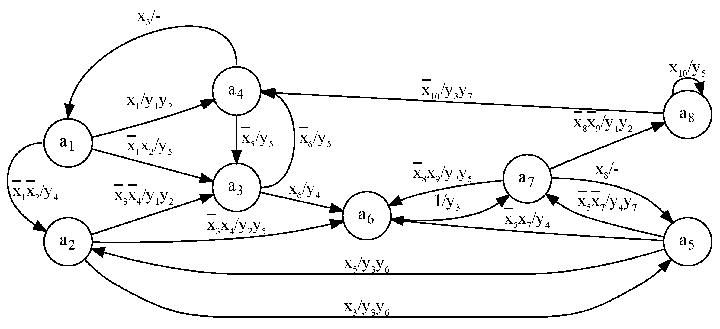
5. Example of Synthesis
We use the symbol
to show that the model of
Mealy FSM (
Figure 4) is used to implement the circuit of an FSM
. Consider an FSM
represented by its STG (
Figure 5). Let us synthesize the circuit of Mealy FSM
using 5-LUTs.
Step 1. The h-th edge of an STG is transformed into a row of an STT [
14]. There are 19 edges in the STG (
Figure 5). So, it should be
rows in the corresponding STT. The transformation is executed in a trivial way [
1].
Table 1 is a resulting STT of FSM
. The following sets can be derived from
Table 1: the set of states
, the set of inputs
, and the set of outputs
. This gives the following parameters:
,
, and
.
Step 2. Using the methods [
17], we can obtain the partition
with
. There are the following classes of this partition:
and
. So, there is
. Using (
12), we can obtain the value
. Using (
13), we can obtain the value
. Now, we have the sets
,
, and
.
Step 3. As known [
2], the state codes do not affect the number of LUTs in circuits of FSMs based on twofold or extended state codes [
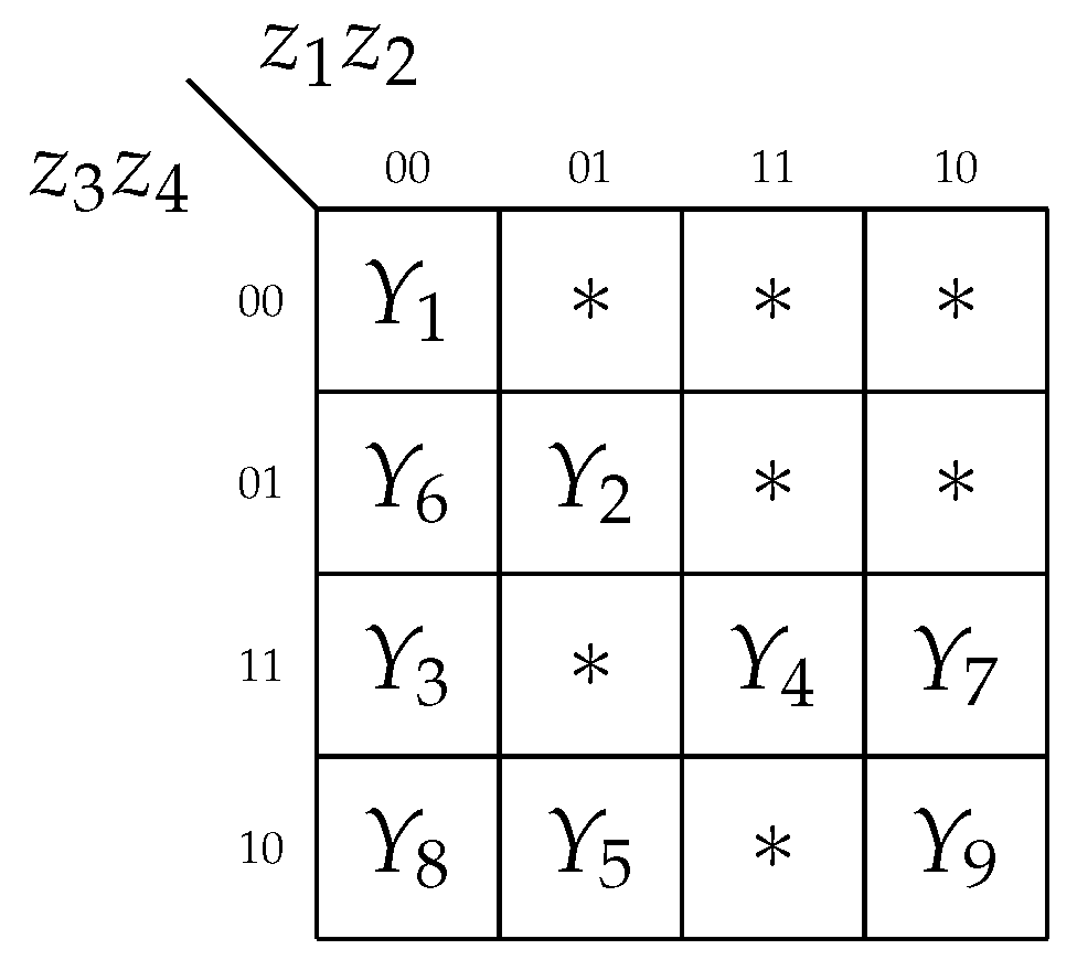
35]. So, the states can be encoded in the arbitrary way. For our example, one of the possible outcomes of the state assignment is shown in
Figure 6.
The following class and state codes can be found from
Figure 6:
and
,
. Using the codes of classes of compatible states
and state codes
gives the following complex state codes:
and
.
Step 4. To execute the replacement, we should find the minimum value of additional variables,
G. To do it, we use the methods from [
14]. It is necessary to analyze sets
including FSM inputs which determine the transitions from states
[
2]. These sets can be found using either the STG (
Figure 5) or STT (
Table 1). In the discussed case, there are the following sets:
and
. If
is a number of elements in the set
, then
.
The value of G is equal to the maximum value of . Obviously, there is . So, it is enough additional variables to replace inputs: .
The columns of table of inputs’ replacement are marked by FSM states
, the rows are marked by additional variables
. If an input
is replaced by a variable
in a state
, then this input is written at the intersection of the corresponding column and row. Using methods from [
14] gives the table of replacement (
Table 2).
Step 5.Table 2 is a base for finding SBF (
5). The following SBF can be derived from
Table 2:
In (
21), the symbol
stands for a conjunction of state variables corresponding to the state
. Obviously, each of Equation (
21) can be implemented as
.
Step 6. There are
different collections of outputs in STT (
Table 1). They are the following:
.
To optimize the circuit of
, it is necessary to encode COs in a way minimizing the total number of literals in SBF (
7) [
2]. Each literal determines an interconnection between
and
. Using the approach from [
2], we can encode the COs as it is shown in
Figure 7.
Step 7. Using contents of COs and their codes (
Figure 7) gives the following SBF:
There are 16 literals in (
22). The maximum number of literals is equal to
. So, due to encoding shown in
Figure 7, the number of literals (and interconnections) has almost halved.
Step 8. The DST of
Mealy FSM is constructed using the initial STT, codes of states and COs, and a table of replacement of inputs. A DST includes the following columns:
,
,
,
,
,
,
,
h. The columns of state codes include codes from
Figure 6. The column
is constructed using the initial STT and table of replacement of inputs (
Table 2). The column
includes IMFs equal to 1 for loading the code
into state register. The column
includes variables
equal to 1 in the code
of CO written in the
h-th row of STT. This column is constructed using the initial STT and codes of COs (
Figure 7).
In the discussed case, the DST is represented by
Table 3. Let us analyze the first row of
Table 3. There is the input
in this row of
Table 1. As follows from
Table 2, the input
is replaced by the additional variable
in the state
. For this row, there is the following relation:
. As follows from
Figure 6, there is
. Due to this, column
of
Table 3 contains
in row
. In row 1 of
Table 1, there is the CO
in column
. As follows from
Figure 7, there is
. Due to this, column
of
Table 3 contains
in row
. All other rows of
Table 3 are constructed in the same way.
Step 9. These tables are constructed using the classes
, DST of
Mealy FSM, codes
and
. For the discussed example, there is
. So, there are two blocks (
and
) generating the partial functions (
16) and (
17). The transitions from the states from the class
are represented by
Table 4, for the class
by
Table 5.
There is a transparent correspondence between
Table 3, on the one hand, and tables of
(
Table 4) and
(
Table 5), on the other hand. There are
rows in
Table 4 and
rows in
Table 5. Obviously, the following equality takes place:
.
Step 10. The following sets can be found from
Table 4 and
Table 5:
,
, and
. It means that each
contains
5-LUTs. Together, this gives 14 5-LUTs in the mutual circuit of
and
.
The functions (
16) and (
17) are constructed in the trivial way. For example, the following SBF of partial functions
, and
can be derived from
Table 4 and
Table 5:
All other partial functions are created in the same manner.
Step 11. The table of
is constructed using sets
and
where
. The table contains the columns "Function" and "j". For our example, this block is represented by
Table 6.
For example, the IMF appears in both tables. Due to this, there are ones in columns with and . All other rows are filled used the similar analysis.
Step 12. The SBFs (
18) and (
19) representing the third level of the logic circuit are constructed in the trivial way. They include two components: (1) conjunctions of variables
corresponding to class codes and (2) corresponding partial functions. For example, functions
and
are represented by the following SBF:
All other functions (
18) and (
19) are constructed in the same manner.
Step 13. To implementing the LUT-based circuit of Mealy FSM
, it is necessary to use some CAD tools. In the case of FPGAs from Virtex-7, the system Vivado [
31] should be used; for our simple example we can design this circuit manually.
As follows from (
21), there are nine literals in the sum-of-products of
and eight literals in the sum-of-products of
. The circuit should be implemented using LUTs with
inputs. So, the condition (
4) holds. To implement the circuit of
, it is necessary to apply the methods of FD [
12,
13]. As a result, we obtain a two-level circuit of
including six LUTs.
In the discussed case, each function
is represented by
partial functions. Further, the condition (
11) holds for the blocks of
. Due to this, there are enough
5-LUTs for implementing the circuits of
-
. Since
, there are seven LUTs in the circuit of
. As follows from (
22), there are seven LUTs in the circuit of
.
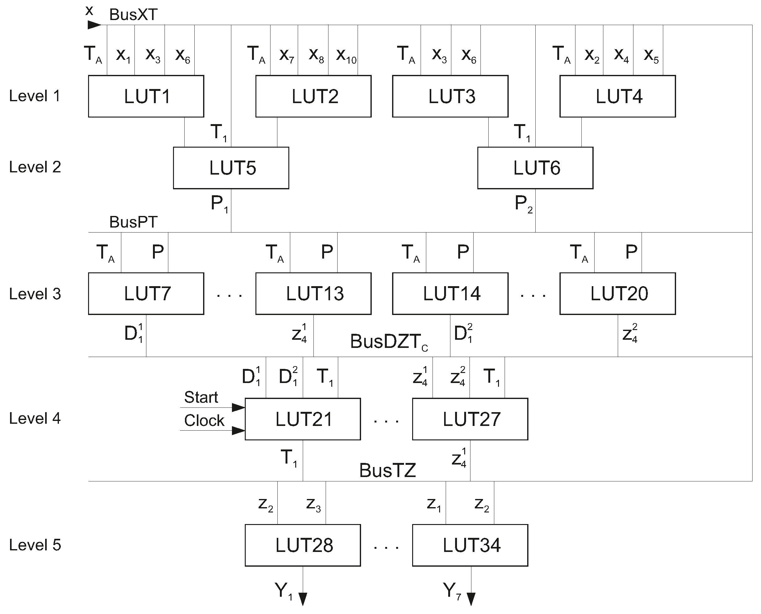
So, there are 34 5-LUTs in the circuit of Mealy FSM
. This circuit has five levels of LUTs (
Figure 8).
In this circuit,
is represented by LUT1–LUT6. This circuit has two levels of LUTs shown in
Figure 8. The
delivers the inputs
and state variables
for generating the additional variables
. These variables enter
to be transformed into the partial functions (
16) and (
17). The transformation is executed by
and
. These blocks include elements LUT7–LUT20. The fourth level of the FSM circuit is represented by LUT21–LUT27. The IMFs are generated by LUT21–LUT23. The outputs of these LUTs are connected with flip-flops implementing the register RG. The flip-flops are controlled by the pulses
and
. The variables
are generated by LUT24–LUT27. The outputs of
form the
. At last, level five consists of seven LUTs (LUT28–LUT34) creating the circuit of
.
We compared the characteristics of the 5-LUT-based circuits of and FSMs. In both cases, there is the same number of flip-flops in the state register (). In the case of , there are six LUTs in the and seven LUTs in . There are two levels of LUTs in the circuit of . So, these subcircuits are the same for and . There are two levels of LUTs in the circuit of of . This block’s circuit includes 24 LUTs. So, there are LUTs in the circuit of .
Thus, for the FSM , the transition from model to model allows you to reducing the LUT count by 1.088 times. Note that both circuits have the same number of logical levels; therefore, the model proposed in this article allows reducing the number of LUTs without reducing the operating frequency compared to the circuit of equivalent FSM. In the next Section, we compare some FSM models with the one proposed in this article.
6. Experimental Results
In this Section, we show the results of experiments which have been conducted to compare characteristics of
Mealy FSMs with characteristics of FSM circuits based on some other models. To conduct the experiments, we use: (1) the internal resources of Virtex-7; (2) the benchmark FSMs from the library [
36]; (3) the industrial package Vivado [
31]. The library [
36] includes 48 benchmarks represented in the format KISS2. The benchmarks have a wide range of basic characteristics (numbers of states, inputs, and outputs). They are used very often by different researchers to compare area and time characteristics of FSMs obtained using various synthesis methods. The characteristics of benchmarks are shown
Table 7.
We executed the experiments using a personal computer with the following characteristics: CPU: Intel Core i7 6700 K 4.2@4.4 GHz, Memory: 32 GB RAM 2400 MHz CL15. Further, we used the Virtex-7 VC709 Evaluation Platform (xc7vx690tffg1761-2) [
37] and CAD tool Vivado v2019.1 (64-bit) [
31]. There is
for FPGAs of Virtex-7. To obtain the results of experiments, the reports produced by Vivado are used. To enter Vivado, we use thed CAD tool K2F [
2].
We compared three basic characteristics of resulting FSM circuits. These parameters are: (1) the LUT count; (2) the time of cycle; (3) the power consumption. In addition, two integral characteristics were investigated, namely: (1) the area-time products and (2) the area-time-power products. To conduct the experiments, five FSM models were used. They are: (1) Auto of Vivado (it uses binary state codes); (2) one-hot of Vivado; (3) JEDI; (4)
-based FSMs; (5)
-based FSMs proposed in this article. Obviously, the first three methods are based on the model of
P FSM shown in
Figure 2.
Based on the methodology [
35], we divide the benchmark FSMs [
36] by five categories. To divide the benchmarks, we use the relation between the values of
and
. There is
for LUTs of Virtex-7. We use this value to divide the benchmarks by the categories.
The benchmarks belong to category of trivial FSMs (category 0), if the following condition holds: . This category includes the following 11 benchmarks: and . The benchmarks belong to category of simple FSMs (category 1), if there is . The category 1 consists of the benchmarks bbara, bbsse, beecount, cse, dk14, dk15, dk16, donfile, ex2, ex4, ex6, ex7, keyb, mark1, opus, s27, s386, s840, and . The benchmarks belong to category of average FSMs (category 2), if . The category 2 contains the benchmarks ex1, kirkman, planet, planet1, pma, s1, s1488, s1494, s1a, s208, styr, and . The benchmarks belong to category of big FSMs (category 3), if the following condition takes place: . The category three includes only the benchmark . The category of very big FSMs (category 4) includes benchmarks satisfying relation . The benchmarks s420, s510, s820, and s832 belong to this category.
The results of experiments are shown in
Table 8,
Table 9,
Table 10,
Table 11 and
Table 12. There is the same organization of these tables. The investigated methods are listed in the table columns. The table rows contain the names of benchmarks. Inside each table, the benchmarks are listed in alphabetical order, and sorted by ascending category number. The rows “Total” contain results of summation of values for each column. The row “Percentage” includes the percentage of summarized characteristics of FSM circuits produced by other methods respectively to
-based FSMs. We use the model of
P Mealy FSM as a starting point for methods Auto, one-hot, and JEDI. The basic data (the LUT count, time, and power consumption) are taken from reports of Vivado. Next these data were used to obtain the integral characteristics.
Let us analyze the experimental data taken from reports of Vivado. These tables contain the following data: (1) the LUT counts (
Table 8); (2) the minimum time of cycle (
Table 9); (3) the total On-Chip Power (
Table 10); (4) the area-time products (
Table 11); (5) the area-time-power products (
Table 12). In addition, we compared each of the characteristics for each category; however, in order to avoid a significant increase in the size of the article, we did not show the corresponding tables. We just showed the results of these comparisons.
As follows from
Table 8, the
–based FSMs require fewer LUTs than it is for other investigated counterparts. Using the proposed approach, we can obtain circuits having 52.19% less 6-LUTs than it is for equivalent Auto–based FSMs; 77.1% less 6-LUTs than for equivalent one-hot–based FSMs; 25.34% less 6-LUTs than for equivalent JEDI–based FSMs. Our approach produces circuits having on average 11.36% less 6-LUTs than the circuits of
-FSMs.
Using
Table 8, we can compare LUT counts for different categories of benchmark FSMs. Comparing the results for category 0 shows that both multi-level approaches (
and
) lose out to the other methods. This loss is 30.4% compared to auto-based FSMs, 3.4% compared to one-hot-based FSMs, and 31.5% compared to JEDI-based FSMs. We explain this by the fact that condition (
4) is not satisfied for benchmark FSMs of the category 0. This means that only a single LUT is needed to implement any function for systems (
1) and (
2). Obviously, for category 0, the replacement of inputs should not be performed for both
and
FSMs; however, the encoding of output collections is always performed for these multi-level FSMs. Due to this, for the category 0, the multi-level FSMs have higher LUT counts than they are for other investigated design methods. Let us point out, that equivalent
- and
-FSMs have the same LUT counts for this category.
Starting from category 1, the condition (
4) is met. At the same time, it makes sense to use structural reduction methods instead of methods of functional decomposition. For this category, using the complex state codes in
FSMs allows obtaining FSM circuits with fewer LUTs than it is for other methods used in our experiments. This gain is 40.0% compared to auto-based FSMs, 81.1% compared to one-hot-based FSMs, 16.2% compared to JEDI-based FSMs, and 11.0% compared to
FSMs.
As follows from this part of research, the winnings increase with the increase in the category number. The gain in LUTs increases up to 65.64% (for categories 2–4) compared to auto-based FSMs. The gain increases up to 65.64% (for categories 2–4) compared to one-hot-based FSMs. Comparison with JEDI-based FSMs shows that the gain increases up to 34.86% (for categories 2–4). At last, compared to -based FSMs, the gain increases from 8.44% (for categories 0–1) to 12.73% (for categories 2–4).
As follows from
Table 9, the
-based FSMs are faster than their investigated counterparts. They require a cycle time 9.39% less than the equivalent auto-based FSMs, 10.24% less than one-hot-based FSMs, and 1.08% less than the equivalent JEDI-based FSMs. win 18.73%. They also marginally benefit (0.31%) in relation to
FSMs. It follows from this that our approach allows reducing the number of LUTs without losing performance. As we have already noted, this is the greatest challenge associated with the optimization of chip area occupied by an FSM circuit. So, our approach allows overcoming this obstacle.
Using
Table 9, we have compared time characteristics for different categories of benchmark FSMs. Comparing the results for category 0 shows that
-based FSMs lose out to the other methods. This loss is 3.23% compared to auto-based FSMs, 0.2% compared to one-hot-based FSMs, 3.68% compared to JEDI-based FSMs, and 1.13% compared to
-based FSMs. As it is for LUT counts, we explain this by the fact that condition (
4) is not satisfied for benchmarks of this category. Starting from category 1, the condition (
4) is met. This allows obtaining some gain compared to FSMs based on both Auto (3.48%) and one-hot (3.37%); however, other models provide better performance than our approach (3.84% compared to JEDI and 1.93% compared to
).
Starting from the category 2, our approach gives better results compared to all other investigated methods. This gain for the category 2 is the following: (1) 24.17% compared to Auto; (2) 25.96% compared to one-hot; (3) 8.88% compared to JEDI; (4) 3.78% compared to FSMs. For the category 3, the gain increases. It is the following: (1) 31.49% compared to Auto; (2) 31.49% compared to one-hot; (3) 20.24% compared to JEDI; (4) 4.76% compared to FSMs. Further, there is a gain for category 4; however, the gain is less than for category 3. It is the following: (1) 18.73% compared to Auto; (2) 16.48% compared to one-hot; (3) 7.96% compared to JEDI; (4) 3.07% compared to FSMs. We explain this decrease in winnings by an increase in the number of levels in the circuits of -based FSMs compared to their number for category 3; however, the following conclusion can be drawn: the proposed approach allows obtaining faster LUT-based FSM circuits starting from category 2.
The Vivado provides us by information about the total on-chip power. We combine these reports in
Table 10. As follows from
Table 10, the
-based FSMs consume less energy than their investigated counterparts. On average, they provide the following gain in power consumption: (1) 47.02% compared to auto-based FSMs; (2) 59.17% compared to one-hot-based FSMs; (3) 23.96% compared to JEDI-based FSMs; (4) 5.44% compared to
Mealy FSMs.
Using
Table 10, we have compared total on-chip power for each category. Comparing the results for category 0 shows that
-based FSMs lose out to the other methods. This loss is 19.37% compared to auto-based FSMs, 17.6% compared to one-hot-based FSMs and 21.08% compared to JEDI-based FSMs. The same data are correct for
FSMs; however, starting from the category 1, our approach allows designing circuits consuming less power. The winnings grow as the category number grows. With respect to auto-based FSMs, our method provides the following gain: (1) 33.95% for the category 1; (2) 85.68% for the category 2; (3) 106.28% for the category 3; (4) 124.46% for the category 4. With respect to one-hot-based FSMs, our method provides the following gain: (1) 47.22% for the category 1; (2) 98.26% for the category 2; (3) 106.28% for the category 3; (4) 163.44% for the category 4. With respect to JEDI-based FSMs, the proposed method provides the following gain: (1) 19.69% for the category 1; (2) 43.98% for the category 2; (3) 77.38% for the category 3; (4) 80.97% for the category 4. Further, there is the following gain compared to
-based FSMs: (1) 5.20% for the category 1; (2) 7.58% for the category 2; (3) 10.77% for the category 3; (4) 12.36% for the category 4. So, the proposed organization of the FSM circuit allows reducing the power consumption, starting with simple FSMs (category 1).
Using data from
Table 8,
Table 9 and
Table 10, we can calculate the values for two integral characteristics. One of them is an area-time product [
6,
38], the second is an area-time-power product. The smaller the values of these products, the better the quality of the resulting FSM circuit [
6]. As it is the case in many articles [
6,
38], we estimate the area of an FSM circuit by its LUT count.
As follows from
Table 11, the
-based FSMs have better area-time characteristics than their investigated counterparts. On average, they provide the following gain: (1) 84.13% compared to auto-based FSMs; (2) 113.34% compared to one-hot-based FSMs; (3) 33.41% compared to JEDI-based FSMs; (4) 13.53% compared to
Mealy FSMs. Using
Table 11, we have compared area-time characteristics for each category of benchmark FSMs. As in the previous cases, for category 0 our approach gives the worst results; however, starting from category 1, the benefits of our approach are steadily increasing.
Comparing the results for category 0 shows that -based FSMs lose out to the other methods. This loss is 31.8% compared to auto-based FSMs, 2.88% compared to one-hot-based FSMs, 33.33% compared to JEDI-based FSMs, and 1.1% compared to FSMs; however, starting from category 1, our approach allows designing circuits having smaller values of area-time products than they are for all other approaches. With respect to auto-based FSMs, our method provides the following gain: (1) 46.49% for the category 1; (2) 107.13% for the category 2; (3) 90.73% for the category 3; (4) 141.9% for the category 4. With respect to one-hot-based FSMs, our method provides the following gain: (1) 88.39% for the category 1; (2) 139.36% for the category 2; (3) 90.73% for the category 3; (4) 148.74% for the category 4. With respect to JEDI-based FSMs, the proposed method provides the following gain: (1) 11.42% for the category 1; (2) 45.42% for the category 2; (3) 50.63% for the category 3; (4) 61.03% for the category 4. Further, there is the following gain compared to -based FSMs: (1) 8.74% for the category 1; (2) 16.92% for the category 2; (3) 13.88% for the category 3; (4) 18.75% for the category 4. So, the proposed organization of the FSM circuit allows reducing the values of area-time products, starting with simple FSMs (category 1).
As follows from
Table 12, the
-based FSMs have much smaller values of area-time-power products than they are for their investigated counterparts. On average, they provide the following gain: (1) 254.69% compared to auto-based FSMs; (2) 325.06% compared to one-hot-based FSMs; (3) 96.36% compared to JEDI-based FSMs; (4) 22.75% compared to
Mealy FSMs. Using
Table 12, we have compared area-time-power products for each category of benchmark FSMs. As in the previous cases, for category 0 our approach gives the worst results; however, starting from category 1, the benefits of our approach are steadily increasing.
Comparing the results for category 0 shows that -based FSMs lose out to the other methods. This loss is 45.51% compared to auto-based FSMs, 10.12% compared to one-hot-based FSMs, 48.69% compared to JEDI-based FSMs, and 1.13% compared to MPY FSMs; however, starting from category 1, our approach allows designing circuits having smaller values of area-time-power products than they are for all other approaches. With respect to auto-based FSMs, our method provides the following gain: (1) 104.39% for the category 1; (2) 301.21% for the category 2; (3) 293.45% for the category 3; (4) 502.86% for the category 4. With respect to one-hot-based FSMs, our method provides the following gain: (1) 194.34% for the category 1; (2) 376.56% for the category 2; (3) 293.45% for the category 3; (4) 528.13% for the category 4. With respect to JEDI-based FSMs, the proposed method provides the following gain: (1) 36.51% for the category 1; (2) 112.16% for the category 2; (3) 167.19% for the category 3; (4) 213.43% for the category 4. Further, there is the following gain compared to -based FSMs: (1) 15.65% for the category 1; (2) 25.71% for the category 2; (3) 26.14% for the category 3; (4) 33.91% for the category 4. So, the proposed organization of the FSM circuit allows reducing the values of area-time-power products, starting with simple FSMs (category 1).
The main goal of the proposed approach is the reducing LUT counts in FPGA-based circuits of Mealy FSMs. The results of experiments (
Table 8) show that this goal has been achieved. Obviously, this gain is achieved by using complex state codes in
FSMs. Using these codes leads to introducing an additional level of LUTs forming the partial functions. It was natural to expect that the introduction of this additional level would lead to a decrease in performance; however, as follows from
Table 9, our approach leads to slower FSM circuits only for FSMs from categories 0–1. As the complexity of FSMs increases, our approach begins to give a win in terms of minimum cycle time. Moreover, the proposed approach allows reducing the power consumption of resulting FSM circuits (starting from the category 1). The same is true for the integral characteristics of FSM circuits (the area-time and area-time-power products). These phenomena are positive side effects associated with our approach.
So, the results of our experiments show that the proposed approach can be used instead of other models starting from the simple FSMs (category 1). Our approach allows improving LUT counts starting from the simple FSMs. The same is true for the power consumption. Further, starting from the category 2, the proposed method allows improving the minimum cycle time compared with other investigated methods. In our research, we use the chip xc7vx690tffg1761-2 by Virtex-7 (Xilinx); however, this chip has no unique architecture of CLBs. This very architecture of CLBs is used in all chips of the 7th generation of Xilinx chips. Due to this, the results of our experiments show that the proposed approach can be used for improving LUT counts for designs based on any FPGA chip of the 7th generation. Moreover, all Xilinx FPGA families have one fundamental property in common: an extremely limited number of LUT inputs. This leads to the need to develop FSM synthesis methods aimed at reducing the influence of this factor on the characteristics of the LUT-based FSM circuits. The results of our research show that the proposed method allows solving this problem better than some well-known methods combining various approaches of state assignment (auto, one-hot, and JEDI) and functional decomposition, as well as our previous method based on structural decomposition ( FSMs).


