Abstract
Near-threshold voltage (NTV) operation has the potential to improve the energy efficiency of digital integrated circuits. However, the use of a conservative timing guard band to avoid the timing errors introduces excessive timing margins, thus causing larger energy dissipation in the NTV region. An error-tolerant design based on timing error detection and correction circuits has been shown to be a promising solution to mitigate these issues. This paper presents a light-weight timing error-tolerant flip-flop (ETFF) design. This design detects timing errors using a node transition signal detector with only nine transistors and corrects these errors during the same clock cycle. Moreover, transistor sizing is explored to optimize the trade-off between performance and area overhead. The proposed ETFFs are inserted into a monitored circuit by replacing original flip-flops at timing-monitored points. To further reduce the overhead, we develop a mean-time-to-failure-aware method to select the monitored points by simultaneously considering the critical path coverage and activation rates of flip-flops. The simulation results show that a CNN accelerator using the proposed timing error-tolerant design implemented in the SMIC CMOS 40 nm process can robustly work at 1.1–0.3 V with only 3.5% area overhead. Furthermore, this design reduces the area overhead by 54.68% and improves the energy efficiency by 53.69% at 0.6 V, compared with the Razor flip-flop design. The advantage of the proposed design lies in that it requires smaller circuit overheads and can work reliably in a wider range of supply voltages.
1. Introduction
Lowering supply voltages to the near-threshold voltage (NTV) region is one of the effective techniques for achieving higher energy efficiency in energy-constrained circuits [1,2,3]. However, NTV operations also cause new challenges due to the increasing delay caused by process, voltage and temperature (PVT) variations under the scaling voltages [2]. These challenges are specifically manifested as: (1) over 10× loss in performance, (2) 5× increase in performance variation, and (3) a five-order of magnitude increase in the functional failure rate of memory and logic circuits [3]. Moreover, the PVT-induced variations affect both the clock signals and data paths, so the critical paths may fail to deliver the output data within the given clock period [4]. Furthermore, timing errors in data paths cannot be tolerated by masking because the delay of bit flipping will be recurrently accumulated in circuits such as the multiply-accumulate (MAC) units in a neural network (NN) processor [2]. Thus, the propagation of timing errors incurs a significant accuracy loss, especially in the deep neural network (DNN) accelerators containing a large number of MACs [5].
Conventional integrated circuit designs avoid the PVT-induced timing errors by reserving voltage and timing margins as a timing guard band. However, the conservative guard band causes the reduction in throughput and excessive cost of energy wasting [5], because a circuit does not always work in the worst case. Timing error-tolerant techniques based on the error detection and correction (EDAC) circuits have emerged as a promising solution [2,3,4,5,6,7,8,9,10,11,12,13,14,15,16,17,18,19,20,21,22,23,24,25,26,27]. The EDAC designs use the timing error detection (TED) circuits to monitor the timing conditions of circuits at run time. The timing error correction (TEC) circuits are designed to recover the timing errors resulting from the delay violations. Thus, the high operation frequency can be retained under the lower supply voltages. Moreover, the EDAC design can be used with the adaptive voltage frequency scaling technique to eliminate the excessive voltage and timing margins, further saving the energy consumption [3,25,26].
The EDAC designs have been researched for many NN accelerators [2,3,5,6,7,8,9,10,11,12,19,20,27] and the circuits of microprocessors [13,14,15,16,17,18,21,22,23,24,25,26]. One prominent EDAC design is the Razor flip-flop (RFF) [13]. An RFF detects timing errors by comparing the outputs of a shadow latch and the main master-slave flip-flop (MSFF). It corrects timing errors by refreshing the instruction and redoing operations. However, the TED design of the RFF causes considerable circuit costs in power and area. The TEC design increases the constraint of the hold time, which makes the TEC design of the RFF unsuitable for NTV operations [1].
In order to expand the operating voltage range and achieve a higher energy efficiency, we improved and extended our previous work [27]. In this paper, a timing error tolerant flip-flop (ETFF) is proposed and applied in the processing element (PE) circuits of a convolutional NN (CNN) accelerator, as shown in Figure 1. An ETFF consists of a node transition signal detector (NTSD) using only nine transistors and a data selection error correction unit (DSEC). The NTSD monitors the timing conditions by detecting the wrong transitions of nodes, which are caused by delay violations. Once the delay of a circuit violates the timing constraints as the supply voltage reduces, the NTSD will immediately generate an error signal. The DSEC is designed based on a conventional transmission-gate flip-flop (TGFF) [28] and two extra transmission gates. The DSEC driven by error signals from the NTSD will then select valid input data to recover the timing errors during the same clock cycle.
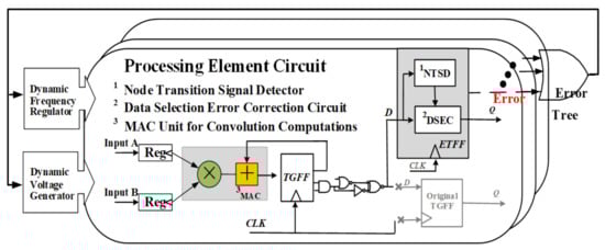
Figure 1.
A PE circuit using the proposed ETFF design in a CNN accelerator.
Compared to our previous work [27], the improvement and extension introduces the following two novelties: (1) Transistor sizing for the proposed ETFF is explored to further improve the trade-off between power, delay and area. The lowest supply voltage that the proposed ETFF steadily works at is extended to 0.3 V. (2) The proposed TEC design of the ETFF is simplified and improved to retain the robust edge-sampling characteristic of a master-slave flip-flop with only two extra transmission gates. The main contributions of this work are as follows:
- A light-weight timing error-tolerant circuit, namely, the ETFF, is designed to extend the lowest operation voltage to 0.3 V with a 25.63% area reduction compared with the RFF design [13].
- Transistor sizing is used to improve the power-delay product (PDP) of the proposed ETFF by 9.16–99.84% at supply voltages of 1.1–0.3 V.
- Benefiting from the proposed EDAC design, a CNN accelerator implemented in the SMIC COMS 40 nm process can reliably perform the classification at the supply voltages in the NTV region with an energy saving of up to 55.29%.
2. Background and Related Work
2.1. Timing Issues in NTV Operation
Recent research in the area of near-threshold operations has shown that voltage scaling is a promising energy-efficient technique [1,2,3,5]. The energy dissipation in CMOS circuits is largely caused by the charging and discharging of the internal node capacitance and can be reduced by lowering the supply voltage (denoted by VDD) in a quadratic manner. The threshold voltage is denoted by VT. However, when the voltage is scaled down to the near-threshold (i.e., VDD~VT) and sub-threshold voltage (i.e., VDD < VT) region, the propagation delay variations mainly caused by the drain current can dramatically increase by 50–100× [1] compared to that in the nominal voltage operations. In a compact model [29], the propagating delay tp and the energy of a gate egeat operating under NTV for the 65 nm CMOS process can be respectively expressed as:
where IC, α and σ represent the inversion coefficient, switching activity and drain-induced barrier lowering factor, respectively. Ktp and kfit are the delay-fitting and model-fitting parameters. CL, Cox, VDD and VT represent the load capacitance, the oxide capacitance, the supply voltage and the threshold voltage, respectively. W and L represent the width of the transistors in the driving stage and the channel length, respectively.
The total energy consumed by a gate is the sum of the switching energy and leakage energy during a clock period. One factor of the path delay depends on the technology, transistor sizing and gate topology, while the other depends on the supply and threshold voltage [1]. Thus, NTV operation leads to a several-order of magnitude improvement in the energy efficiency of a circuit. However, the propagation delay is extremely sensitive to the change of the VDD under NTV.
The schematic of a common sequential circuit is shown as Figure 2a. The minimum clock cycle required for a sequential circuit depends on the delay of logic circuits in the worst case, while also accounting for the clock skew due to the routing direction and the location of the clock source. As discussed in [30], the timing constraints are given by
where the clock jitter delay is ignored, and T, tsu and tc-q represent the clock period, setup time and the propagation delay between the clock and output signals, respectively. TCLK2−TCLK1 represents the delay difference of clock signal propagating from the clock tree to sequential circuits and is the maximum delay of combinatorial logic circuits. So, the increase in and due to supply voltage scaling and PVT variations will violate the constraints in (3), then cause delay violations.
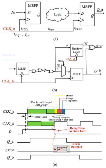
Figure 2.
(a) Conventional circuit design. (b) Timing error-tolerant design RFF [13]. (c) The timing diagram of main signals with nominal and late arriving inputs.
Moreover, the propagation delay becomes more unpredictable and affects the performance more severely under NTV, resulting from unstable PVT variations [26]. A small change in the supply voltage will cause a large change in the delay. Furthermore, with the continuous process technology scaling, a PVT-induced delay increasingly exacerbates the timing conditions of synchronous circuits on both the clock signals and data paths [23]. Thus, the accuracy of logic circuits significantly reduces, resulting in the propagation of intolerable timing errors. Timing guard band is reserved in conventional designs to avoid PVT-induced timing errors, as the CLK_a shows in Figure 2c. However, this conventional method cannot overcome the problem of considerable energy wasting caused by the reserved voltage and timing margins.
2.2. EDAC Circuits
2.2.1. Timing Error Detection
EDAC designs can be classified into three groups by different TED methods:
1. Double sampling comparison (DSC): This method generates error signals by using a comparator to compare the twice samplings driven by the different clock signals. An RFF [13] consists of an XOR gate as the comparator, an MSFF driven by the clock signal of CLK_b and a shadow latch driven by the CLK_d signal, which with a delay is later than the CLK_b signal, as shown in Figure 2b. The RFF concurrently samples the input data by the MSFF based on the structure of a TGFF [28] and shadow latch. If the input signal is late arriving with a delay, the comparator will estimate that the twice samplings are the same and generate error signals. However, an RFF requires more than 20 extra transistors, resulting from the structure of the XOR gate and shadow latch. Moreover, the circuit of the clock pulse generation is required to control the clock duty ratio to activate the shadow latch. This additional circuit adds significant increase in power and complexity to the design.
Sharma et al. proposed a modified design [14], which uses a main latch instead of the MSFF and an XNOR gate as the comparator to reduce the power consumption and enable the lowest supply voltage down to 0.4 V with an operation frequency of 5 MHz. Bowman et al. proposed another modified design named time-borrowing latch (DSTB) [15], which is used in a fully connected DNN (FC-DNN) accelerator [16]. The DSTB sets the output of a latch instead of the MSFF as the transmitted data on the sequential path of circuits and slightly reduced clock energy overhead compared with the RFF design. The study [17] uses a latch to replace the MSFF in [15] to design a scannable error-detection cell (SEDC). The SEDC design used 14 transistors to perform the TED and one extra multiplexer, causing additional power. Moreover, the time borrowing (TB) technique discussed in Section 2.2.2 is required for the TEC operation of the designs [15,16,17], which causes considerable energy consumption.
2. Error prediction (EP): This method generally introduces a margin Δt by using some buffers to anticipate possible delay violations. Sato et al. uses a main flip-flop sampling the data first and a canary flip-flop [18] sampling the data a time Δt later. When comparing both values by an XOR gate, the error prediction assumes the last sample of the flip-flop is correct. If the input data arrives later, these two values will not be the same and the XOR gate will generate an error signal. The canary design [18] has been used to realize a low power DNN accelerator [19]. Jain et al. designed the multi-bit flip-flop [20] based on the error prediction method, which has high tolerance against soft errors. A simplified design is designed in [20], which just uses a delay chain instead of a canary flip-flop and an XOR-gate to implement the error prediction.
3. Dynamic data transition detection (DDTD): This method generates the error signals by capturing the abnormal transition of node signals caused by delay violations. This transistor-level detection method used in [10,12,22,23,24] has a significant improvement in area and power, compared with the DSC method. However, most of these previous designs can only work at the super-threshold voltage (i.e., 0.8–1.2 V). The design in [10] uses a parity checking monitor to detect the error transition. A transistor as a capacitor with a big discharge capacitance is added to enable this design to stably work at a lower supply voltage (0.57 V) in a 40 nm process. The design named the EDSU in [23] includes two internal nodes with the inverse phases of floating nodes in a circuit by using two high skewed invertors. Four extra transistors are also required in the EDSU to detect the unmoral transition of the floating nodes caused by the input with delay violations. However, the operation voltage of the EDSU can only be down to 0.85 V and the TB technique is required for the TEC operation. Zhang et al. proposed the iRazor design [24], which detects timing errors based on the node signal transition of a latch with only three extra transistors. It can scale the supply voltage down to 0.6 V. However, this design requires six stacked transistors manufactured by the customized material to ensure its stability at a lower voltage.
The EP method used in [18,19,20,21] does not need the operation of the TEC, which reduces the implementation complexity. Thus, this method is fundamentally different from the DSC and DDTD methods. However, it still requires redundant input copies, delay buffers and a comparator, the same as the DSC method, while the DDTD method does not need those. Thus, in comparison with the other two methods, the DDTD method generally has the smallest implementation complexity for the TED operation. Moreover, the delay of buffers in the EP-based designs has to satisfy timing constraints, limiting the increase in energy efficiency. Furthermore, voltage and timing margins are still needed in the EP-based designs, because the main part never causes timing errors. Thus, power reduction caused by the EP method is less than those resulting from the DSC method [15]. However, the clock controller is required in the DSD-based designs to generate the CLK-d signal, which increase the implementation complexity and power dissipation.
2.2.2. Timing Error Correction
After detecting the timing errors, the RFF corrects these errors based on instruction re-execution, driving a multiplier (MUX) to restore valid data with the penalty of one extra clock cycle [4,14]. The iRazor design [24] uses the stalling mechanism to suspend the corresponding cycles with error signals. This TEC design with the cost of one extra clock cycle increases the hold time constraint, which makes it unsuitable for NTV operations [1]. Moreover, any instruction re-execution or stalling in an MAC unit will cause this MAC to go out of synchrony with the remaining MACs in the NN accelerator, leading to incorrect computation [11].
The TB technique [15] performs the TEC operation by borrowing time from the next pipeline stages, instead of instruction re-execution. It has been introduced into the data paths of NN accelerators in the studies [2,8,9,16,22]. The TB technique depends on the assumption that the time borrowed is absorbed by a non-critical path in the next stage. However, this assumption may not be valid and cause the further propagation of timing errors, especially in high-performance designs [22]. Moreover, a complex circuit of the clock controller is required to perform the time borrowing, resulting in considerable energy consumption.
With increasing research into the field of the energy-efficient NN, the TE-Drop technique has been proposed as a new TEC method for NN accelerators [3,6,7]. The main idea of the TE-Drop is dropping or skipping the operations of erroneous MACs instead of recovering them [19], ignoring the possible loss in accuracy. The study in [10] employs both the TE-Drop and TB technique in the tensor processing unit (TPU) and obtains up to 57% energy saving.
2.3. Monitored Point Selection
By replacing endpoint flip-flops (FFs) of critical paths with EDAC circuits, a common method inserts EDAC circuits into application processors. This method chooses critical paths with a timing slack smaller than 10–20% of the clock period, mostly depending on a static timing analysis (STA). For example, the RFFs used in a FC-DNN accelerator [2] result in an area overhead of 13.6%. In [12], the top 503 most critical registers are augmented for timing error detection, out of a total of 2976 ones. This represents that approximately 17% of the total FFs are replaced by the EDAC circuits with 6.9% area overhead and 5.7% power overhead. The designs used in [24,25] select 19.8% endpoint FFs and 70% critical paths (with 7.8% area overhead) as the monitor points, respectively. Thus, the problem of these considerable circuit costs in area and power caused by EDAC circuits is a real obstacle for area and energy-constrained mobile applications.
Moreover, the slack of some noncritical paths close to the critical paths’ slack increases under PVT variations. In other words, the noncritical paths are prone to becoming critical paths in a real condition. The variability of some noncritical paths caused by the unpredictable delay has to be considered. It has become an unavoidable challenge when applying EDAC circuits into DNN accelerators with a mass of parallel MAC units [2]. For instance, a TPU-like array with roughly 65 K MACs has a 50% global timing error rate, even if each MAC unit only experiences 5–10 timing errors in each clock cycle. Therefore, there is a need to design a high-efficiency monitored point selection method to reduce the area and power overheads and simultaneously monitor potentially critical paths.
3. Proposed Timing Error-Tolerant Flip-Flop
In this section, the structure and principle of the proposed light-weight EDAC design ETFF are illustrated. The ETFF uses a node transition signal detector (NTSD) with only nine extra transistors to detect the timing errors. These errors are corrected in the same clock cycle by the proposed data selection error correction (DSEC) unit. Moreover, in order to use fewer EDAC circuits to realize more effective timing detection, a mean-time-to-failure-aware hybrid selection (MAHS) method is proposed, considering the variability in noncritical paths.
3.1. Node Transition Signal Detector (NTSD)
The proposed NTSD circuit consists of seven transistors denoted by M1–M7, respectively, and one skewed inverter denoted by I8. The schematic and operation of the NTSD are presented in Figure 3 and Table 1. M7 controlled by the clock signal donated by CK is used as the detection window regulator. It determines if the NTSD works at the range of the high clock phase. During the low clock phase, M7 is switched on, keeping the signal of the FVDD node in logic-high. When the clock pulse is high and M7 is switched off, the FVDD node becomes a floating node. Once the transitions of the input signal denoted by D occur, the voltage at the FVDD node will immediately drop and I8 will generate a timing error signal.
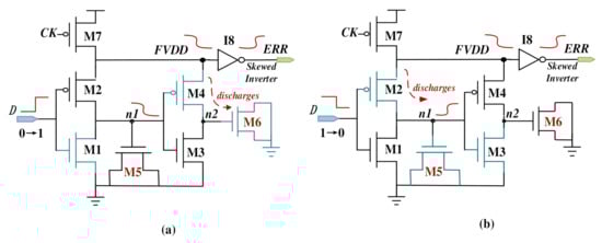
Figure 3.
The schematic and operation of the proposed NTSD: (a) the input data D transitions from logic “0” to “1”; (b) the input data D transitions from logic “1” to “0”.

Table 1.
Operation of the proposed NTSD design.
The timing error detection principle of the NTSD, under two input data transition scenarios, is explained in detail below. As shown in Figure 3a and Table 1, when D is logic “0”, M2 and M3 are switched on. So, the FVDD node will be in the logic-high state, the same as the internal node denoted by n1. The internal node denoted by n2 will stay in logic-low under the normal transmission without a timing error. Once D transitions from logic “0” to “1”, M2 is abruptly switched off, n1 is discharged to logic-low state and M4 is switched on. However, the floating node FVDD will be discharged to logic-low because n2 is discharged by M6 to stay in logic-low for a short time.
When the input D is logic “1”, M1 and M4 are switched on, as shown in Figure 3b. So, the FVDD node and n2 stay in logic-high, n1 will stay in logic-low under the normal transmission. Once D transitions from logic “1” to “0”, M4 is abruptly switched off and the floating node FVDD will be discharged to logic-low state, because n1 discharged by M5 will be in logic-low for a short time. Then, I8 connected to FVDD will promptly capture the voltage change and generate the timing error signal.
To ensure these abrupt transitions can be immediately detected under NTV, the NMOS transistor M5 and M6 are used as a discharge tube to make the node n1 or n2 stay in logic-low for sufficient time. Otherwise, the floating node FVDD will not be fully discharged to active I8 to generate a timing error signal. Consequently, it requires a higher ratio of width to length to ensure the discharge characteristics of M5 and M6.
The sizing issues in the proposed transistor level design are analyzed as follows. During the detection phase, the voltage at the floating node FVDD will drop due to the charge-sharing effect. These charges will flow from node FVDD and n2 through M4 and M6 to VSS when the input signal D changes from logic “0” to “1”, or from node FVDD and n1 through M2 and M5 to node VSS in another case, as shown in Figure 3. The proposed design detects delay errors by capturing the discharge state of the floating node FVDD. Thus, three techniques can be applied to improve the functionality and robustness of the proposed design.
- The inverter I8 requires skewed transistor sizing to ensure that it has a sufficiently high logic threshold voltage regardless of process corners.
- The node capacitance at n1 and n2 must be increased through the transistor sizing to support sufficient charges.
- The transistor sizes of M5 and M6 must be enlarged to ensure the fast and sufficient voltage reduction at the floating node FVDD and a successful logic switch occurs at the node denoted by ERR.
Notably, all of these design techniques must consider the effects of extra area consumption and delay exacerbation under serious NTV PVT variations. Moreover, a limited and varying voltage swing leads to a small noise margin and large delay penalty in the skewed inverter I8. These concerns render the design of this NTSD challenging. The transistor sizing process for I8, M5 and M6 is explored to improve the energy efficiency and enable the proposed EDAC design to robustly work at NTV, as discussed in Section 3.3.
3.2. Data Selection Error Correction (DSEC)
The DSEC circuit based on the structure of the conventional TGFF [28] is composed of two latches and two transmission gates denoted by G1 and G2, as shown in Figure 4. G1 and G2 are driven by error signals from the NTSD to select the valid inputs. Under the nominal timing conditions, when the system circuits work without timing errors, G1 stays switched on and G2 stays switched off.
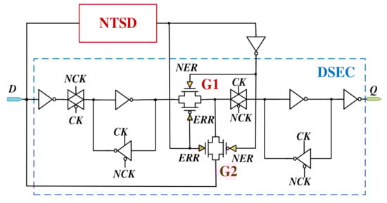
Figure 4.
The schematic of the proposed ETFF.
Once the transition of input signal caused by delay violations occurs, the NTSD will generate an error signal and transmit it to G1 and G2. G1 will be promptly switched off and G2 will become transparent to select the valid input signal after late transition. Then, the output of the slave latch denoted as Q will follow the valid input signal through G2.
Combining the DSEC circuit with the NTSD, the ETFF is designed. The schematic of the proposed ETFF is shown in Figure 4. As a direct result, the proposed ETFF retains the edge-sampling characteristic of a master-slave flip-flop with the abilities of detecting and correcting timing errors. Characteristics of the proposed ETFF compared to the RFF design [13] and standard TGFF cell [28] working at 0.6 V are shown in Table 2. The ETFF with merely nine extra transistors only has 1.7× area overhead and 1.59× switching energy of the standard TGFF, compared with the RFF design which has 2.3× area overhead and 2.12× switching energy of the TGFF. Moreover, this design has a shorter average error detection delay and does not need one extra clock cycle to reload valid data from memory circuits, compared with the RFF design. This further improves the efficiency of application circuits.
Table 2.
Characteristics of the proposed ETFF compared to the Razor [13] and TGFF [28] at 0.6 V under TT process corner @ 25 °C.
3.3. Transistor Sizing
To ensure the inverter I8 to capture a subtle voltage dropping at the floating node FVDD, I8 requires skewed transistor sizing to have a sufficiently high logic threshold voltage. We investigate the impact of inverse narrow PMOS width effect [31] on the threshold voltage at different supply voltages with SMIC 40 nm HVT process technology. The results are shown in Figure 5a, indicating that the variation of threshold voltage increases as the supply voltage decreases. The threshold voltage of the inverter remains nearly flat for transistor width larger than 400 nm but decreases quickly as the transistor width approaches the minimum width (W = 120 nm). To minimize the area overhead, we set the width of the PMOS transistor in the skewed inverter I8 as 400 nm.
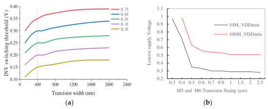
Figure 5.
(a) VT of the inverter with different PMOS transistor sizing. (b) The lowest operating voltage of the NTSD with different sizing of M5 and M6.
The lowest operating voltage of the NTSD decreases as the width of M5 and M6 increases, as shown in Figure 5b. At the operation frequency of 10 MHz, the lowest operating voltage remains nearly flat when the width of M5 and M6 transistors increases to larger than 500 nm. At the operation frequency of 100 MHz, the lowest operating voltage remains nearly flat when the width of M5 and M6 increases to larger than 800 nm.
Figure 6 indicates that the delay of timing detection decreases at the supply voltages of 1.1–0.3 V as the width of transistors M5 and M6 increases. The change in the delay of the NTSD is insignificant when the width of transistors is larger than 500 nm. As the supply voltage increases from the standard voltage 1.1 V to the NTV, the delay of the NTSD increases much more quickly than expected due to drain current increasing.
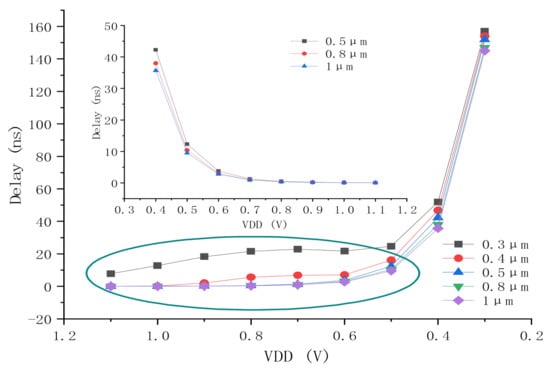
Figure 6.
The delay of timing detection with various transistor sizing and supply voltages.
Simulation results in Table 3 present the performances of average power, worst case delay and the PDP of the proposed NTEE with the different sizes of M5 and M6 at supply voltages of 1–0.3 V. The 9.16–99.84% reduction in the PDP indicates the effectiveness of transistor sizing method. Although the delay in the worst case increases with the voltage scaling, the PDP reduces and the reduction trend gradually decreases as the width of M5 and M6 increases. These precipitously change at a supply voltage of 0.5 V (almost NTV). Thus, the proposed ETFF achieves the lowest PDP at the supply voltage of 0.5 V, although the power saving reduces 5× compared with the lowest supply voltage of 0.3 V.
Table 3.
The power, delay and PDP of the proposed ETFF with transistor sizing.
3.4. Proposed MTTF-Aware Hybrid Selection (MAHS) Method
Considering the variability in noncritical paths, we introduce the mean-time-to-failure (MTTF) constraint [32] to propose an MTFF-aware hybrid selection (MAHS) method. This method simultaneously considers the coverage and activation rates of all FFs instead of only circuit paths. The constraints of the MTTF and the circuit cost in area (the number of the monitored points) are also considered to select the final monitored registers in application circuits.
The automatic flow using the proposed MAHS method is presented in Figure 7. The STA and VCS dynamic simulations are performed to output the information of the FFs, data paths and timing conditions of the monitored circuit. Then, the FFs are sorted by the values of the covered paths and activation rate, by using the python script. All of the FFs on the data paths are scanned to find the FFi with the maximal coverage rate, until the number of data paths covered by the FFs is not smaller than 60% of all data paths. After activation rates of FFs are scanned, an FF with an activation rate larger than 60% will be selected even if it has a path coverage rate less than 60%.
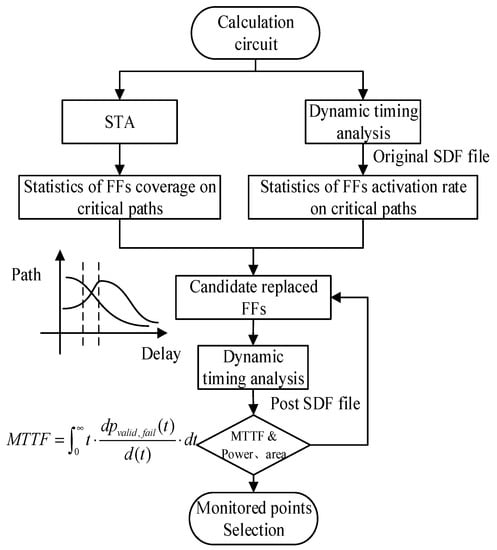
Figure 7.
An automatic design flow of the proposed MAHS algorithm.
As shown in Figure 8, the node B with the same path coverage as node A is selected as the candidate FF, because it has a higher activation rate over the node A. The node D with a smaller activation rate will not be chosen, although its path coverage rate is larger than 60%. The coverage-rate-based and activation-rate-based selections are iteratively performed to obtain all candidate FFs to be replaced. In the processing element (PE) array circuits of baseline CNN accelerator, we select 28 FFs covering 874 paths and 59 FFs with 60% activation rates among a total of 831 FFs on 874 paths. Finally, the proposed MAHS method chooses 39 FFs, thus reducing 25 FFs with 3.5% area and 2.17% power savings, compared with the common method choosing endpoints of critical paths with a timing slack smaller than 10% of the clock period.
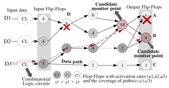
Figure 8.
Illustration of the MAHS sifting monitor points.
Iizuka et al. proposed a stochastic framework to estimate the MTTF constraint by modeling the circuit operation as a continuous-time Markov process [32]. The state transition probability denoted as Pi,j (s, t) that the circuit is in state i at time s and will stay in state j at time t is given by:
In the case of a stationary Markov process, pi,j (s,t) can be simply expressed as pi,j (t). Q-matrix using qi,j (the transition rate of the leaving state i) is expressed by:
Let denote the eigenvalue matrix of Q-matrix, and denotes the corresponding eigenvector matrix of Q-matrix. Then, the matrix of state transition probability can be expressed by:
The state transition probability being at state fail at time t from the state valid, denoted by Pvalid,fail which is computed by (6), so the MTTF of a circuit can be calculated by:
To further verify the effectiveness of the MAHS algorithm, we also applied it to the ISCAS’89 benchmark circuits [33], in addition to the PE array of baseline 40 nm CNN accelerator. The comparison results are listed in Table 4, where the common selection method selects FF endpoints of critical paths with a timing slack smaller than 10% of the clock period. The comparison results indicate that the proposed selection method can perform better area overhead saving implemented in larger test processors with complicatedly interlaced data paths. Furthermore, the proposed ETFFs inserted in circuits using the MAHS method can obtain an area reduction of 2.7–29.8% and save 5.65% power, compared with the RFF design [13] using the common selection method.
Table 4.
The number of monitored points selected by different methods in ISCAS’89 benchmark circuits [33] and the circuit of a CNN accelerator.
4. Application and Performance Analysis
The structure design and operating principle details of the proposed light-weight timing error-tolerant design, namely, ETFF, have been described in Section 3. To verify the effectiveness of area and power savings, we applied the proposed ETFF design in a CNN accelerator. Moreover, the circuit-level comparison details with other EDAC designs are discussed.
4.1. Experiment Setup
The circuit of a CNN accelerator based on the classic LeNet-5 model [34] for digit classification is implemented as a baseline circuit by using the SMIC 40 nm process. This baseline circuit consists of a 4 × 4 processing element (PE) array, external and internal memory units (input and output FIFO and weight buffers), data transfer bus and parameter configuration unit. Each PE circuit is composed of a 16-bit fixed multiplier and adder (1/3/12 fixed) and the input and output registers built based on the structure of the TGFF. The proposed ETFF has been inserted in the circuit of data paths by replacing an original TGFF, as shown in Figure 1. The parameters of this baseline CNN model are trained by Python with 10,000 images in the MNIST dataset. The accuracy of classification inferred by using accurate adders is 98.73%.
The hardware prototype of the baseline accelerator is implemented in RTL Verilog and synthesized using the Synopsys Design Compiler. The layout of the proposed ETFF design is generated by using the Cadence Virtuoso, following the standard cell design rules defined by the SMIC 40 nm process technology, as shown in Figure 9. Moreover, buffers are added for input signals and a load of a fanout-of-4 inverter (FO4) is used at the output, to simulate a real environment. The output load of the FO4 is also considered for power and delay evaluation. The parasitic parameters netlist is extracted by the Mentor Graphics Calibre. The ETFF cell has been inserted into the standard cell library, after the post-layout simulation has been conducted. The STA and VCS simulations are performed to analyze the static and dynamic timing.

Figure 9.
Layouts for the proposed (a) NTSD and (b) ETFF.
4.2. Performance Analysis
The EDAC functions and performances of delay, switching energy and average power of the proposed ETFF design are evaluated by using HSPICE simulator under scaling supply voltages, which have been discussed in Section 3. Furthermore, to verify the robustness, exhaustive 10 k Monte Carlo (MC) simulations with 3-sigma process variation are performed for a wide voltage range of 0.2–1.1 V and the frequency range of 0.5–10 K MHz. The timing waveforms of main signals are displayed in Figure 10, where the transitions of the input signal D from logic “0” to “1” and from logic “1” to “0” are all introduced. Figure 10 presents the 10 K MC results for the voltage of 1.1, 0.6, 0.4 and 0.3 V at a frequency of 500, 100, 5, and 1 MHz, respectively. When the voltage is scaled to 0.3 V at the frequency of 1 MHz, there is enough timing margin, allowing further increase in operation frequency or throughout. However, significant noises appear in the FVDD signal and the error signal, as shown in Figure 10d. These noises will affect the EDAC function and the output signal, if the supply voltage is further reduced. The simulation results indicate that the lowest operating voltage of the ETFF can be scaled to 0.3–0.6 V.
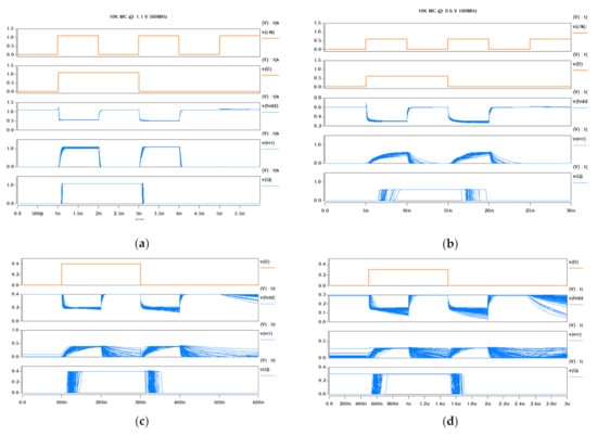
Figure 10.
The results of 10 K MC simulations: (a) at 1.1 V, 500 MHz; (b) at 0.6 V, 100 MHz; (c) at 0.4 V, 5 MHz; (d) at 0.3 V, 1 MHz.
By replacing original FFs at monitored points selected by using the proposed MAHS method, 39 ETFFs are inserted into the PE array circuits of a CNN accelerator. Voltage scaling is also performed on CNN accelerator circuits to estimate the effectiveness and efficiency of the proposed ETFF design. The energy saving of up to 55.27% compared with the baseline circuit has been obtained without any loss in classification accuracy, when the operation voltage is scaled down to 0.5 V at the operating frequency of 100 MHz.
Table 5 shows the characteristics of the proposed ETFF design and other EDAC designs applied in NN accelerators. In comparison with other EDAC designs, the proposed ETFF causes a small area overhead of only 3.5%, because it uses only nine extra transistors and less monitored points. Although the design in [16] based on the TEC method of the DSTB [15] and TB [22] has less area overhead compared with ours, the proposed design brings the largest energy saving (55.27% overall energy saving at 0.5 V), benefiting from light-weight design and voltage scaling. Moreover, the proposed design reduces area overhead by 54.68% and improves energy efficiency by 53.69% at 0.6 V, compared with the design in [13], as discussed in Section 3.2.
Table 5.
The characteristics of the proposed ETFF design and other EDAC designs applied in NN accelerators.
5. Conclusions
In this paper a light-weight timing error detection and correction circuit design, namely, ETFF, is proposed to increase energy efficiency by scaling supply voltages down to the near-threshold voltage region. This transistor-level design utilizes a node transition signal detector with only nine transistors to detect timing errors. These errors can be immediately recovered by data selection based on the proposed error correction design during the same clock cycle. Moreover, transistor sizing is used to optimize the trade-off between performance and overheads and enable the ETFF to stably work in a wider voltage range of 1.1–0.3 V. Furthermore, monitored points are selected by using the proposed MAHS method that simultaneously considers the coverage and activation rates of all flip-flops instead of only those on circuit paths with a timing slack smaller than 10–20% of the clock period. A baseline CNN accelerator using the SMIC 40 nm process can reliably operate under near-threshold voltages, benefiting from the proposed design and leading to 55.27% overall energy saving at 0.5 V. Additionally, the power overhead of timing error-tolerant circuits can also be considered in the selection of monitored points in further work. The proposed light-weight design can be more efficient in saving energy for larger circuits. As an example, deep neural network accelerators with a massive number of layers and weights that have to be recurrently calculated would benefit from the proposed design and will be considered in future work.
Author Contributions
Conceptualization, X.F. and H.L. (Hao Liu); methodology, X.F.; software, X.F. and H.L. (Hongwei Li); validation, J.H., X.F. and H.L. (Hongwei Li); formal analysis, J.H., X.F. and H.L. (Hongwei Li); investigation, X.F.; resources, H.L. (Hao Liu) and S.L.; data curation, X.F.; writing—original draft preparation, X.F.; writing—review and editing, X.F., H.L. (Hongwei Li); S.L. and J.H.; visualization, X.F.; supervision, J.H. and H.L. (Hao Liu); project administration, H.L. (Hao Liu) and X.F.; funding acquisition, H.L. (Hao Liu) and J.H. All authors have read and agreed to the published version of the manuscript.
Funding
This research was funded by the fundamental research funds for the central universities, grant number 3206002204C3 and the Natural Sciences and Engineering Research Council (NSERC) of Canada, grant number RES0048688. The APC was funded by Project 8506006040.
Acknowledgments
This work is supported by the fundamental research funds for the central universities under Project 3206002204C3 and the Natural Sciences and Engineering Research Council (NSERC) of Canada under Project RES0048688. Xuemei Fan is supported financially by the state-sponsored scholarship program administered by the China Scholarship Council (CSC).
Conflicts of Interest
The authors declare no conflict of interest.
References
- Dreslinski, R.G.; Wieckowski, M.; Blaauw, D.; Sylvester, D.; Mudge, T. Near-threshold computing: Reclaiming Moore’s Law Through Energy Efficient Integrated Circuits. Proc. IEEE 2010, 98, 253–266. [Google Scholar] [CrossRef]
- Whatmough, P.N.; Lee, S.K.; Brooks, D.; Wei, G.-Y. DNN Engine: A 28-nm Timing-Error Tolerant Sparse Deep Neural Network Processor for IoT Applications. IEEE J. Solid-State Circuits 2018, 53, 2722–2731. [Google Scholar] [CrossRef]
- Kim, S.; Cerqueira, J.P.; Seok, M. A Near-Threshold Spiking Neural Network Accelerator with a Body-Swapping-Based In Situ Error Detection and Correction Technique. IEEE Trans. Very Large Scale Integr. VLSI Syst. 2019, 27, 1886–1896. [Google Scholar] [CrossRef]
- Agwa, S.; Yahya, E.; Ismail, Y. ERSUT: A Self-Healing Architecture for Mitigating PVT Variations without Pipeline Flushing. IEEE Trans. Circuits Syst. II Express Briefs 2016, 63, 1069–1073. [Google Scholar] [CrossRef]
- Shin, D.; Choi, W.; Park, J.; Ghosh, S. Sensitivity-Based Error Resilient Techniques with Heterogeneous Multiply–Accumulate Unit for Voltage Scalable Deep Neural Network Accelerators. IEEE J. Emerg. Sel. Top. Circuits Syst. 2019, 9, 520–531. [Google Scholar] [CrossRef]
- Zhang, J.; Rangineni, K.; Ghodsi, Z.; Garg, S. Thundervolt: Enabling Aggressive Voltage Underscaling and Timing Error Resili-ence for Energy Efficient Deep Learning Accelerators. In Proceedings of the 55th Annual Design Automation Conference, San Francisco, CA, USA, 24–28 June 2018. [Google Scholar]
- Pandey, P.; Basu, P.; Chakraborty, K.; Roy, S. GreenTPU: Improving Timing Error Resilience of a Near-Threshold Tensor Pro-cessing Unit. In Proceedings of the 56th ACM/IEEE Design Automation Conference (DAC), Las Vegas, NV, USA, 2–6 June 2019. [Google Scholar]
- Zhang, J.; Ghodsi, Z.; Garg, S.; Rangineni, K. Enabling Timing Error Resilience for Low-Power Systolic-Array Based Deep Learning Accelerators. IEEE Des. Test 2019, 37, 93–102. [Google Scholar] [CrossRef]
- Whatmough, P.N.; Lee, S.K.; Lee, H.; Rama, S.; Brooks, D.; Wei, G. A 28 nm SoC with a 1.2 GHz 568nJ/Prediction Sparse Deep-Neural-Network Engine with >0.1 Timing Error Rate Tolerance for IoT Applications. In Proceedings of the IEEE International Solid-State Circuits Conference (ISSCC), San Francisco, CA, USA, 5–9 February 2017; pp. 242–243. [Google Scholar]
- Ghosh, A.; Naseem, M.S.; Kumar, C.I. Time-Borrowing Flip-Flop Architecture for Multi-Stage Timing Error Resilience in DVFS Processors. In Proceedings of the 2021 International Conference on Intelligent Technologies (CONIT), Hubli, India, 25–27 June 2021. [Google Scholar] [CrossRef]
- Fan, X.; Wang, R.; Zeng, Q.; Liu, H.; Lu, S. A Simple Steady Timing Resilient Sample Based on Delay Data Sense Detection. In Proceedings of the 2019 IEEE 13th International Conference on ASIC (ASICON), Chongqing, China, 29 October–1 November 2019. [Google Scholar] [CrossRef]
- Bull, D.; Das, S.; Shivashankar, K.; Dasika, G.S.; Flautner, K.; Blaauw, D. A Power-Efficient 32 bit ARM Processor Using Timing-Error Detection and Correc-tion for Transient-Error Tolerance and Adaptation to PVT Variation. IEEE J. Solid-State Circuits 2010, 46, 18–31. [Google Scholar] [CrossRef]
- Das, S.; Roberts, D.; Lee, S.; Pant, S.; Blaauw, D.; Austin, T.; Flautner, K.; Mudge, T. A Self-Tuning DVS Processor using Delay-error Detection and Correction. IEEE J. Solid-State Circuits 2006, 41, 792–804. [Google Scholar] [CrossRef]
- Sharma, P.; Das, B.P. Design and Analysis of Leakage-Induced False Error Tolerant Error Detecting Latch for Sub/Near-Threshold Applications. IEEE Trans. Device Mater. Reliab. 2020, 20, 366–375. [Google Scholar] [CrossRef]
- Bowman, K.A.; Tschanz, J.W.; Kim, N.S.; Lee, J.C.; Wilkerson, C.B.; Lu, S.-L.L.; Karnik, T.; De, V.K. Energy-Efficient and Metastability-Immune Resilient Circuits for Dynamic Variation Tolerance. IEEE J. Solid-State Circuits 2008, 44, 49–63. [Google Scholar] [CrossRef]
- Lee, S.K.; Whatmough, P.N.; Brooks, D.; Wei, G.Y. A 16-nm Always-On DNN Processor with Adaptive Clocking and Multi-Cycle Banked SRAMs. IEEE J. Solid-State Circuits 2019, 54, 1982–1992. [Google Scholar] [CrossRef]
- Zhang, H.; He, W.; Sun, Y.; Seok, M. An Area-Efficient Scannable In Situ Timing Error Detection Technique Featuring Low Test Overhead for Resilient Circuits. In Proceedings of the 2021 IEEE/ACM International Conference On Computer Aided Design (ICCAD), Munich, Germany, 1–4 November 2021. [Google Scholar] [CrossRef]
- Sato, T.; Kunitake, Y. A Simple Flip-Flop Circuit for Typical-Case Designs for DFM. In Proceedings of the 8th International Symposium on Quality Electronic Design (ISQED’07), San Jose, CA, USA, 26–28 March 2007; pp. 539–544. [Google Scholar] [CrossRef]
- Zhang, J.; Garg, S. FATE: Fast and Accurate Timing Error Prediction Framework for Low Power DNN Accelerator Design. In Proceedings of the 2018 IEEE/ACM International Conference on Computer-Aided Design (ICCAD), San Diego, CA, USA, 5–8 November 2018. [Google Scholar]
- Jain, A.; Veggetti, A.M.; Crippa, D.; Benfante, A.; Gerardin, S.; Bagatin, M. Radiation Tolerant Multi-Bit Flip-Flop System with Embedded Timing Pre-Error Sensing. IEEE J. Solid-State Circuits 2022, 57, 2878–2890. [Google Scholar] [CrossRef]
- Uytterhoeven, R.; Dehaene, W. Design Margin Reduction Through Completion Detection in a 28-nm Near-Threshold DSP Processor. IEEE J. Solid-State Circuits 2021, 57, 651–660. [Google Scholar] [CrossRef]
- Choudhury, M.; Chandra, V.; Mohanram, K.; Aitken, R. TIMBER: Time Borrowing and Error Relaying for Online Timing Error Resilience. In Proceedings of the DATE, Dresden, Germany, 8–12 March 2010. [Google Scholar] [CrossRef]
- Hao, Z.; Xiang, X.; Chen, C.; Meng, J.; Ding, Y.; Yan, X. EDSU: Error Detection and Sampling Unified Flip-Flop with Ultra-Low Overhead. IEICE Electron. Express 2016, 13, 20160682. [Google Scholar] [CrossRef]
- Zhang, Y.; Khayatzadeh, M.; Yang, K.; Saligane, M.; Pinckney, N.; Alioto, M.; Blaauw, D.; Sylvester, D. iRazor: Current-Based Error Detection and Correction Scheme for PVT Varia-tion in 40-nm ARM Cortex-R4 Processor. IEEE J. Solid-State Circuits 2017, 53, 619–631. [Google Scholar] [CrossRef]
- Zhou, J.; Liu, X.; Lam, Y.H.; Wang, C.; Chang, K.H.; Lan, J.; Je, M. HEPP: A New In-Situ Timing-Error Prediction and Prevention Technique for Variation-Tolerant Ultra-Low-Voltage Designs. In Proceedings of the IEEE Asian Solid-State Circuits Conference (A-SSCC), Singapore, 11–13 November 2013; pp. 129–132. [Google Scholar]
- Shan, W.; Shang, X.; Shi, L.; Dai, W.; Yang, J. Timing Error Prediction AVFS With Detection Window Tuning for Wide-Operating-Range ICs. IEEE Trans. Circuits Syst. II Express Briefs 2017, 65, 933–937. [Google Scholar] [CrossRef]
- Fan, X.; Li, H.; Li, Q.; Wang, R.; Liu, H.; Lu, S. A Light-Weight Timing Resilient Scheme for Near-Threshold Efficient Digital ICs. In Proceedings of the IEEE Asia Pacific Conference on Circuits and Systems (APCCAS), Ha Long, Vietnam, 8–10 December 2020; pp. 133–136. [Google Scholar]
- Markovic, D.; Nikolic, B.; Brodersen, R.W. Analysis and Design of Low-Energy Flip-Flops. In Proceedings of the IEEE International Symposium on Low Power Electronics and Design (ISLPED), Huntington Beach, CA, USA, 6–7 August 2001; pp. 52–55. [Google Scholar]
- Markovic, D.; Wang, C.C.; Alarcon, L.P.; Liu, T.-T.; Rabaey, J.M. Ultralow-Power Design in Near-Threshold Region. Proc. IEEE 2010, 98, 237–252. [Google Scholar] [CrossRef]
- Maheshwari, N.; Sapatnekar, S. Timing Analysis and Optimization of Sequential Circuits; Springer Science & Business Media: Berlin/Heidelberg, Germany, 1998. [Google Scholar]
- Zhou, J.; Jayapal, S.; Busze, B.; Huang, L.; Stuyt, J. A 40 nm Dual-Width Standard Cell Library for Near/Sub-Threshold Operation. IEEE Trans. Circuits Syst. I Regul. Pap. 2012, 59, 2569–2577. [Google Scholar] [CrossRef]
- Iizuka, S.; Masuda, Y.; Hashimoto, M.; Onoye, T. Stochastic Timing Error Rate Estimation Under Process and Temporal Variations. In Proceedings of the IEEE International Test Conference (ITC), Anaheim, CA, USA, 6–8 October 2015. [Google Scholar]
- Brglez, F.; Bryan, D.; Kozminski, K. Combinational Profiles of Sequential Benchmark Circuits. In Proceedings of the IEEE Inter-national Symposium on Circuits and Systems, Portland, OR, USA, 8–11 May 1989; pp. 1929–1934. [Google Scholar]
- Lecun, Y.; Bottou, L.; Bengio, Y.; Haffner, P. Gradient-based Learning Applied to Document Recognition. Proc. IEEE 1998, 86, 2278–2324. [Google Scholar] [CrossRef] [Green Version]
Publisher’s Note: MDPI stays neutral with regard to jurisdictional claims in published maps and institutional affiliations. |
© 2022 by the authors. Licensee MDPI, Basel, Switzerland. This article is an open access article distributed under the terms and conditions of the Creative Commons Attribution (CC BY) license (https://creativecommons.org/licenses/by/4.0/).