Abstract
All-metal 3D printing technologies are allowing the conception of new structures for different applications. This publication explores the potential of employing for the first time an all-metal 3D unit-cell topology to perform wide-angle impedance matching layers. A new equivalent circuit is derived for the oblique incidence, providing a good estimation of the cell response for the scanning range () in the main scanning planes for a linearly polarized radiated field. This analytical model is later used to develop a wide-angle impedance matching design methodology for a generic antenna. This methodology is tested in practice to match a phased array made of metallic horns at 18 GHz. An improvement of 5 dB is obtained in the simulations for angles for the H-plane.
1. Introduction
Wide scanning capabilities are usually required when using radar systems, modern communication systems, such as in 5G applications [1], or communications with low earth orbit (LEO) satellites [2]. As it is well known, while steering the beam, the coupling between the elements in the array may deteriorate the antenna active matching, possibly resulting in scan blindness [3]. It is particularly difficult to conceive an element for a phased array that scans at a wide angle, because its periodicity has to be smaller than to avoid grating lobes. Some methods have been developed to avoid these problems, such as the use of mechanical steering [4]. Other methods try to alleviate the problem while allowing for electrical scanning, which consist of the use of matching networks in the antenna elements [5], reconfigurable active structures [6,7] or matching layers placed above the antenna. Such layers are commonly known as wide-angle impedance matching (WAIM) surfaces. This article proposes an innovative topology and the associated design methodology for a WAIM that can be built employing only metal. Indeed, 3D additive manufacturing methods allow to build a full structure in just one metallic piece, avoiding the use of connections or welds that could cause problems or deformations in the final response, as well as increasing the fabrication process speed. In addition, it avoids the use of dielectric materials in the structure, preventing problems such as intrinsic losses in these materials and the outgassing phenomenon [8] that dielectrics may suffer when they are used in space.
The use of these innovative manufacturing technologies results in a large number of 3D all-metal structures that are used in a wide range of applications. It can be found in frequency selective surfaces (FSS) acting as spatial filters [9,10,11], or as polarizers [12,13,14], metallic antennas [15,16,17] as well as metallic arrays [18,19,20]. Lenses are also being made as 3D metallic structures [21,22,23] and microwave filters as well [15,24]. To the best knowledge of these authors, there is no proposal for a metallic WAIM in the literature yet.
Classical WAIM solutions can be classified according to their topology, such as single dielectric layers [25,26,27,28], single layer metamaterials [29,30,31,32,33], multilayer metamaterials [34,35,36] and 3D WAIMs [37]. Their design methodologies can also be classified into those that make use of optimization algorithms during all of the design process [30,34,38], or others that use an equivalent circuit (EC) [29,36,37] with which the cell is modeled. The optimization algorithms take into account all the degrees of freedom from a unit-cell and adjust them until obtaining the desired response. On the other hand, the ECs change the geometrical parameters of the unit-cell according to the EC elements required (an optimization process is also present but at the end of the design). This strategy is very useful to know the response of the global structure (antenna plus WAIM) without the need for a full-wave simulation, which highly reduces the computing time and the needed resources.
It should be noted that other alternative techniques (analytical and quasi-analytical) have been proposed in the literature to model the discontinuities in waveguides or open structures [39,40]; however, they have not been considered here for the sake of simplicity.
The WAIM proposed in this article is based on a 3D structure that has been proposed by some of the authors [14]. It works as a simple waveguide that allows the excitation of low dispersive transverse-electromagnetic (TEM) modes. Thus far, the structure has been employed as a polarizing radome, and it was modeled by an EC that was only valid for normal incidence. In order to synthesize the WAIM, this paper proposes an improved EC that also accounts for the incident angle. This extension is a great contribution because characterizing the structure for oblique incidence is necessary for WAIM applications. For the methodology presented in this publication, a specific radiating element has been used, but the methodology is valid for any other element. This paper is organized as follows. Section 2 describes the topology that is used for the WAIM application and its characterization in an EC conceived to work with oblique incidence. Section 3 explains the methodology developed to design a WAIM layer. Finally, Section 4 shows the general conclusions of this contribution and the possible next steps.
2. Proposed Unit-Cell and Equivalent Circuit
2.1. Description of the Structure
The basic unit-cell considered in this manuscript is based on the structure proposed by some of the authors in [14], consisting of an innovative periodic cell that supports TEM modes when illuminated by an impinging wave under normal incidence. It is formed by four metallic corners, as it is sketched in Figure 1a. Such a structure was employed in [12] to design a polarizing screen. For the purpose of designing a WAIM, the unit-cell can be loaded by a shunt impedance placed at the loading plane (as it was also performed in [14] in order to synthesize the polarization conversion and to provide physical support to the four metallic corners, because they are floating).

Figure 1.
TEM unit-cell: (a) general structure, (b) incidence planes considering Y polarization.
The interest in using this kind of 3D unit-cell is to benefit from its multiple degrees of freedom, broad operation bandwidth and avoidance of dielectric materials. The possibility to interact independently with the fields impinging in the two main scanning planes (H- and E-planes, taking as reference the Y polarization like in Figure 1b) is particularly appealing for the WAIM application.
2.2. Description of the EC
Figure 2 depicts the proposed EC for the generic cell in Figure 1a. The cell is part of an infinite periodic array excited by a plane wave under oblique incidence (defined by the angle, in one of the principal planes). This field is vertically polarized (electric-field component parallel to y axis).
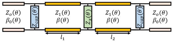
Figure 2.
EC of a generic loaded unit-cell with θ dependence.
The EC mainly consists of two transmissions line of length + , describing the propagation of a TEM vertical mode in the quasi-parallel-plate waveguide (PPW) formed by the opposite pairs of metal corners on top and bottom (separated by the horizontal slits of width ). and are, respectively, the characteristic impedance and phase constant of this line. Shunt impedances are used to mimic the discontinuities at the input and output, whilst stands for the possible shunt load placed in the loading plane along the cell length.
The propagation constant inside the cell related to the fundamental mode has a different expression depending on the incident plane. It can be approximated analytically assuming the cell behaves as an infinite PPW. In the H-plane (), the wave vector inside the unit-cell remains the same as the incident wave vector in free space, whatever. Thus, it divides into two components, and. The propagation constant, corresponding to, can be expressed as in Equation (1), being the working frequency (18 GHz) and the speed of light.
However, in the E-plane (), the wave vector inside the cell does not have any component (as enforced by the incident wave vector in free space). Then, the propagation constant is the unique component, whose value is shown in Equation (2).
This important difference also suggests that the mismatching at the entrance of the cell is stronger for the E-plane, especially when increases. Indeed, in this case, the component of the incident wave vector is not compatible with the propagation within the PPW, which may lead to increased reflection.
This EC can be seen as an extension of the one shown in [14], that was limited to normal incidence. By taking into account the dependency on for most of the EC elements, this upgraded EC is now suitable to WAIM applications where oblique incidence gets compulsory for scanning.
2.3. Derivation of Circuit Elements
The numerical evaluation of the circuit elements is performed in two steps. First, the EC of the unit-cell without the central load is analyzed to extract the characteristic impedance of the transmission line and the input/output discontinuity shunt impedances. In a second step, the load is added to the unit-cell and the shunt impedance, produced by this load, is extracted. All the circuit elements are extracted for each and incident plane.
For the unloaded case, the S-Parameters of the cell for each incident plane and angle are first computed with full-wave simulations under infinite periodic conditions. A circuit simulator (Keysight ADS) is then used to fit the circuit elements, so they best match the full-wave S-Parameters.
Once the circuit elements have been obtained for the unloaded case, the same process is followed with the loaded case to obtain the value of.
2.4. EC Validation
As a validation example, a unit-cell is designed at. It has the following geometrical parameters: (metal thickness)andwhere The validation of the EC is performed comparing the unit-cell full-wave S-Parameters with the EC S-Parameters. The considered frequency band is [13,14,15,16,17,18,19] GHz. This validation is realized for five angles and both E- and H-planes.
Firstly, the validation of the EC for the unit-cell without any load is shown in Figure 3. These results show a very good agreement for all values and for both scanning planes.

Figure 3.
Reflection coefficient validation unloaded unit-cell: (a,b) H-plane and (c,d) E-plane, magnitude and phase, respectively.
The second example is the cell loaded by two vertical columns in the loading plane of the cell as in Figure 4, with the geometrical parameters:and.
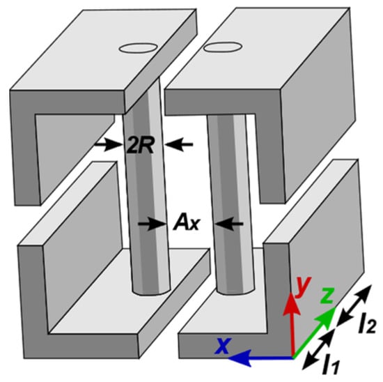
Figure 4.
TEM unit-cell with loads.
The results are shown in Figure 5. These results also show a quite good agreement for the five cases and for both incident planes, although the discrepancy with the full-wave simulations is a bit larger. The mutual coupling between the load and the input/output discontinuities may affect the accuracy of the EC, especially because the cell length is quite small. Moreover, the modeling does not account for the real dimensions of the columns (especially their radius R), as it assumes the loading is concentrated in a single vertical plane along the cell.

Figure 5.
Reflection coefficient validation loaded unit-cell: (a,b) H-plane and (c,d) E-plane, magnitude and phase, respectively.
The load used in this example mostly produces an inductive effect. As varies from 0° to 55°, the extracted changes from 60j to 54j in the H-plane, while in the E-plane, it does not depend on the angle. Therefore, for the sake of simplicity, in the next section, it is considered that does not depend on.
3. WAIM Design Methodology
This section makes use of the previous EC for designing a WAIM placed above a generic antenna to be matched.
3.1. General Design Methodology
Figure 6 depicts the global EC of one array element extracted from an infinite periodic phased array together with its associated WAIM, as represented in Figure 7b. Note that the phased array scans the radiating beam, producing the oblique incidence on the WAIM. Henceforth, the corresponding incident direction is named the scanning direction. It is defined by and, where is either equal to 0 (H-plane in previous section) or , (E-plane). Here, the periodicity of the WAIM unit-cell is the half of an individual array element, which means each array element is covered by four WAIM unit-cells (Figure 7a). The array element is represented by a 2-port network expressing the power exchanges between its feeding port and the fundamental radiated Floquet mode. It is assumed that all higher-order modes are evanescent at the frequency of design (array periodicity is less than, being the free-space wavelength at 18 GHz) and they do not contribute to the interactions with the WAIM structure.
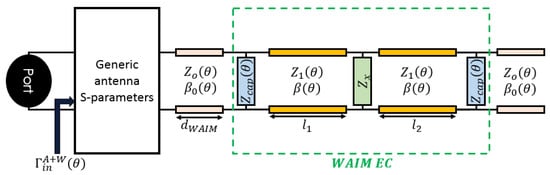
Figure 6.
Global EC: antenna S-Parameters plus space between antenna and WAIM plus WAIM EC.
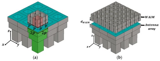
Figure 7.
(a) Phased array of stepped horns with four unit-cells with half-periodicity (one unit-cell represented in red) per one array element (represented in green) (illustrative) and (b) global structure: phased array plus WAIM structure with infinite periodic conditions.
This 2-port network is followed by a transmission line that represents the separation distance between the array and the WAIM (). As will be shown later, this distance is a possible degree of freedom in the design process. The other characteristics of the line, and, are defined by the scanning direction and can be derived analytically. The WAIM with its EC, as defined in Section 2.2, is connected with the 2-port network through this transmission line.
The design methodology can be divided into four main steps. As a preliminary step, a data-base is computed to obtain the circuit elements of the unloaded WAIM unit-cell, using full-wave simulations. It consists of derivingandfor a discretized set of geometries (only varying) and for a discretized set of scanning directions. A full-wave simulation is needed for each geometry and each direction, but these simulations are relatively quick. In the second step, the S-matrix of the array element is also computed using full-wave simulations for the same set of directions. Once again, a new full-wave simulation is needed for each direction.
In the third step, the optimization of the WAIM EC is carried out. To do so, the global EC in Figure 6 is analyzed using a circuit simulator (Keysight ADS) and the possible degrees of freedom (and) are optimized in order to minimize the input active reflection coefficient.
To be noted, the optimization is run for all scanning directions simultaneously, so that, a unique WAIM design is obtained in the end. Moreover, for the sake of simplicity, we assume does not depend on as explained before. Finally, it is important to point out that the choice of enforces the cross-section geometry of the cell. As a consequence, and must be defined correspondently. This is of course automatically managed through the WAIM data-base that opportunely links all interdependent parameters in the EC. On the contrary, andare completely independent degrees of freedom which can be optimized quite freely. It should be emphasized that this optimization step does not require any supplementary full-wave simulation because it is performed with the EC only. This is a definitive advantage of this methodology regarding the huge number of WAIM configurations that may be involved along the successive iterations of the process.
The fourth and last step is a post-processing for. Indeed, the optimization process just provides a theoretical value for the optimal load to be used, together with the cross-section of the cell (defined by as we already have seen). Then, this last step consists of selecting the appropriate load geometry that complies with these outputs. This step relies on the use of a pre-computed data-base, obtained with full-wave simulations as well, that gathers possible candidate loads.
3.2. Application of the Methodology
The methodology is applied for a case where the array element is a metallic horn partially filled in with dielectric (Figure 7a). Thanks to this dielectric, the horn has a periodicity smaller thanat the design frequency, avoiding triggering of grating lobes at maximum angle of scanning.
The active reflection coefficient of the array without the WAIM is shown in Figure 8 in black, and efforts are focused on matching the H-plane, as the matching becomes worse earlier in this scanning direction. The matching of the array is worse than −10 dB for steering angles higher than and in the H- and E-plane, respectively. Following the aforementioned design steps, the optimizable circuit elements for a slit are: and. Figure 8 (red curve) shows the matching in H-plane at is improved by more than 10 dB. Note that the matching in E-plane has been slightly degraded, but it was not considered in the optimization. Next, the load impedance has been synthetized using vertical columns with and, and a full-wave simulation is performed, placing the WAIM as shown in Figure 7b, and yielding green curve in Figure 8. Unfortunately, the performance is not as good as expected, especially in the higher angles. The main reason for the disagreement is the close proximity between the antenna and the WAIM (). This placement of the WAIM in the direct vicinity of the antenna results from the brute optimization process and further investigations demonstrated it was effectively the best solution. However, for such a reduced spacing, the EC is not so accurate due to tight coupling effects. Then, in order to overcome this limitation, a post-processing is applied. Indeed, starting from the EC result, a simple refinement in the radius of the columns is sufficient to improve the final response. By decreasing to, new full-wave results are obtained (blue curve in Figure 8a). These results show significant improvements in the H-plane matching all angles. Furthermore, there is an improvement of more than 5 dB, compared with the initial matching (black curve), in. Such an improvement is not reached in the E-plane.
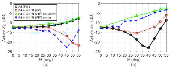
Figure 8.
Active reflection coefficient at f = 18 GHz without limiting : (a) H-plane and (b) E-plane; phased array (PA), full-wave (FW).
Additional Validation
An additional validation is presented to demonstrate that the agreement between full-wave and EC is satisfactory in the case where is not as small as in the previous case. To do so, a re-optimization is conducted where the minimal value of is limited to.
The recalculated circuit elements for the same slit size (are now: The corresponding results are shown in Figure 9 (red curve). As suggested before, the matching improvement in the H-plane is not as good as in Figure 8 because is now limited. However, what is important is that the agreement with full-wave simulation (green curve) is now much better. This suggests the extremely low value of in the previous example was the main reason for a loss of accuracy in the EC prediction. Note that the agreement is quite sensitive to the used value of and, consequently, it might be improved by accounting for its variations with θ.
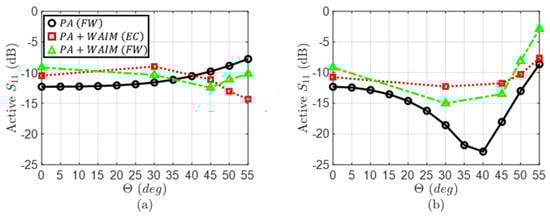
Figure 9.
Active reflection coefficient at limiting : (a) H-plane and (b) E-plane; phased array (PA) and full-wave (FW).
This design can be compared with the literature in Table 1.

Table 1.
Comparison of the proposed design with the literature.
4. Conclusions
In this contribution, a 3D all-metal unit-cell has been characterized for oblique incidence and in the two main scanning planes. Its successful characterization allows its use in applications requiring a wide scanning angle, such as the WAIM application.
Additionally, a new methodology based on the use of an EC has been described, which drastically reduces the total number of needed full-wave simulations. It has been tested with a phased array made of metallic horns, showing a more than 5 dB improvement in the H-plane, for angles larger than 35°. This optimal result was obtained for an extremely small spacing between the WAIM and the antenna, which suggests there could be some interest in integrating the 3D matching structure with the antenna. It was also demonstrated that the agreement provided by the EC gets better when the spacing is increased, due to the used assumptions in the modeling. The methodology may be further improved by following other approaches, such as the mode-matching technique at the cost of increased complexity. Future works will focus on the simultaneous matching of E- and H-planes as well as dual-polarization performance.
Author Contributions
Conceptualization, D.B.-M., M.G.-V., R.G., H.L. and C.M. (Section 2); methodology, D.B.-M., M.G.-V., R.G. and H.L. (Section 3); introduction and conclusion, D.B.-M., M.G.-V. and R.G. (Section 1 and Section 4). All authors reviewed and edited the document. All authors have read and agreed to the published version of the manuscript.
Funding
This publication is supported by the European Union through the European Regional Development Fund (ERDF), and by the french region of Brittany, Ministry of Higher Education and Research, Rennes Metropole and Conseil Departemental 35, through the CPER Project SOPHIE/STIC & Ondes and also by Thales Alenia Space and Region Bretagne.
Conflicts of Interest
The authors declare no conflict of interest.
References
- Tekkouk, K.; Hirokawa, J.; Ando, M.; Sauleau, R. Continuous beam steering antenna with large 2D coverage for 5G applications. In Proceedings of the 2017 IEEE International Symposium on Antennas and Propagation & USNC/URSI National Radio Science Meeting, San Diego, CA, USA, 9–14 July 2017; pp. 243–244. [Google Scholar] [CrossRef]
- Faridani, M.; Xiao, G.; Amaya, R.E.; Yagoub, M.C.E. A Compact Beam-Steerable Integrated Reflectarray Antenna for LEO Applications. In Proceedings of the 2021 IEEE 19th International Symposium on Antenna Technology and Applied Electromagnetics (ANTEM), Winnipeg, MB, Canada, 8–11 August 2021; pp. 1–2. [Google Scholar] [CrossRef]
- Pozar, D.; Schaubert, D. Scan blindness in infinite phased arrays of printed dipoles. IEEE Trans. Antennas Propagat. 1984, 32, 602–610. [Google Scholar] [CrossRef]
- Densmore, A.C.; Jamnejad, V. A satellite-tracking K- and K/sub a/-band mobile vehicle antenna system. IEEE Trans. Veh. Technol. 1993, 42, 502–513. [Google Scholar] [CrossRef]
- Doane, J.P.; Sertel, K.; Volakis, J.L. A Wideband, Wide Scanning Tightly Coupled Dipole Array With Integrated Balun (TCDA-IB). IEEE Trans. Antennas Propagat. 2013, 61, 4538–4548. [Google Scholar] [CrossRef]
- Alibakhshikenari, M.; Virdee, B.S.; Shukla, P.; See, C.H.; Abd-Alhameed, R.A.; Falcone, F.; Limiti, E. Improved adaptive impedance matching for RF front-end systems of wireless transceivers. Sci. Rep. 2020, 10, 14065. [Google Scholar] [CrossRef]
- Valagiannopoulos, C.A.; Monticone, F.; Alù, A. PT-symmetric planar devices for field transformation and imaging. J. Opt. 2016, 18, 044028. [Google Scholar] [CrossRef]
- Gollor, M.; Rogalla, K. HV design of vacuum-insulated power supplies for space applications. IEEE Trans. Elect. Insul. 1993, 28, 667–680. [Google Scholar] [CrossRef]
- Sanz-Izquierdo, B.; Parker, E.A. Frequency selective surfaces formed by partially metalising 3D printed shapes. In Proceedings of the 2015 9th European Conference on Antennas and Propagation (EuCAP), Lisbon, Portugal, 13–17 April 2015. [Google Scholar]
- Liang, B.; Bai, M. Subwavelength three-dimensional frequency selective surface based on surface wave tunneling. Opt. Express 2016, 24, 14697. [Google Scholar] [CrossRef]
- Tang, W.; Zhu, J.; Wang, C.; Ge, J.; Yu, Z.; Zhuang, W. Waveguide 3-D FSSs by 3-D printing technique. In Proceedings of the 2016 International Conference on Electromagnetics in Advanced Applications (ICEAA), Cairns, Australia, 19–23 September 2016; pp. 675–678. [Google Scholar] [CrossRef]
- Molero, C.; Garcia-Vigueras, M. Circuit Modeling of 3-D Cells to Design Versatile Full-Metal Polarizers. IEEE Trans. Microw. Theory Tech. 2019, 67, 1357–1369. [Google Scholar] [CrossRef]
- Molero Jimenez, C.; Menargues, E.; Garcia-Vigueras, M. All-Metal 3-D Frequency-Selective Surface with Versatile Dual-Band Polarization Conversion. IEEE Trans. Antennas Propagat. 2020, 68, 5431–5441. [Google Scholar] [CrossRef]
- Molero, C.; Legay, H.; Pierre, T.; Garcia-Vigueras, M. Broadband 3D-Printed Polarizer based on Metallic Transverse Electro-Magnetic Unit-Cells. IEEE Trans. Antennas Propagat. 2022, 70, 4632–4644. [Google Scholar] [CrossRef]
- Rojas-Nastrucci, E.A.; Nussbaum, J.T.; Crane, N.B.; Weller, T.M. Ka-Band Characterization of Binder Jetting for 3-D Printing of Metallic Rectangular Waveguide Circuits and Antennas. IEEE Trans. Microw. Theory Tech. 2017, 65, 3099–3108. [Google Scholar] [CrossRef]
- Huang, G.-L.; Yuan, T. Application of 3-D metal printing to microwave components and antennas. In Proceedings of the 2017 Sixth Asia-Pacific Conference on Antennas and Propagation (APCAP), Xi’an, China, 16–19 October 2017; pp. 1–3. [Google Scholar] [CrossRef]
- Xiong, Y.; Zhang, B. A Metallic 3D Printed Miniaturized Quasi Log Periodic Koch-Dipole Antenna Using T-Shaped Top Loading. In Proceedings of the 2020 IEEE MTT-S International Microwave Workshop Series on Advanced Materials and Processes for RF and THz Applications (IMWS-AMP), Suzhou, China, 29–31 July 2020; pp. 1–3. [Google Scholar] [CrossRef]
- Zhang, B.; Li, R.; Wu, L.; Sun, H.; Guo, Y.-X. A Highly Integrated 3-D Printed Metallic K-Band Passive Front End as the Unit Cell in a Large Array for Satellite Communication. Antennas Wirel. Propag. Lett. 2018, 17, 2046–2050. [Google Scholar] [CrossRef]
- Foged, L.J.; Giacomini, A.; Morbidini, R.; Saccardi, F.; Schirosi, V.; Boumans, M.; Gerg, B.; Melachrinos, D. Investigation of Additive Manufacturing for Broadband Choked Horns at X/Ku Band. Antennas Wirel. Propag. Lett. 2018, 17, 2003–2007. [Google Scholar] [CrossRef]
- Pfeiffer, C.; Massman, J.; Steffen, T. 3-D Printed Metallic Dual-Polarized Vivaldi Arrays on Square and Triangular Lattices. IEEE Trans. Antennas Propagat. 2021, 69, 8325–8334. [Google Scholar] [CrossRef]
- Yamamoto, T.; Sanada, A.; Kubo, H. Measurements of a 3-D negative refractive index slab lens composed of periodic wired metallic spheres. In Proceedings of the 2011 41st European Microwave Conference, Manchester, UK, 10–13 October 2011. [Google Scholar]
- Diallo, C.D.; Girard, E.; Legay, H.; Sauleau, R. All-metal Ku-band Luneburg lens antenna based on variable parallel plate spacing Fakir bed of nails. In Proceedings of the 2017 11th European Conference on Antennas and Propagation (EUCAP), Paris, France, 19–24 March 2017; pp. 1401–1404. [Google Scholar] [CrossRef]
- Liao, Q.; Fonseca, N.J.G.; Quevedo-Teruel, O. Compact Multibeam Fully Metallic Geodesic Luneburg Lens Antenna Based on Non-Euclidean Transformation Optics. IEEE Trans. Antennas Propagat. 2018, 66, 7383–7388. [Google Scholar] [CrossRef]
- Vallecchi, A.; Cadman, D.; Whittow, W.G.; Vardaxoglou, J.; Shamonina, E.; Stevens, C.J. 3-D Printed Bandpass Filters With Coupled Vertically Extruded Split Ring Resonators. IEEE Trans. Microw. Theory Tech. 2019, 67, 4341–4352. [Google Scholar] [CrossRef]
- Magill, E.; Wheeler, H. Wide-angle impedance matching of a planar array antenna by a dielectric sheet. IEEE Trans. Antennas Propagat. 1966, 14, 49–53. [Google Scholar] [CrossRef]
- Lee, S.; Mittra, R. Radiation from dielectric-loaded arrays of parallel-plate waveguides. IEEE Trans. Antennas Propagat. 1968, 16, 513–519. [Google Scholar] [CrossRef]
- Yun, J.; Park, D.; Jang, D.; Hwang, K.C. Design of an Active Beam-Steering Array With a Perforated Wide-Angle Impedance Matching Layer. IEEE Trans. Antennas Propagat. 2021, 69, 6028–6033. [Google Scholar] [CrossRef]
- Zhou, X.; Wang, M.; Li, Y.; Qiu, C.; Wu, W. Planar Ultra-Wideband Wide-Angle Scanning Array Antenna with Improved WAIM Layer. In Proceedings of the 2021 IEEE International Conference on Power Electronics, Computer Applications (ICPECA), Shenyang, China, 22–24 January 2021; pp. 300–303. [Google Scholar] [CrossRef]
- Cameron, T.R.; Eleftheriades, G.V. Analysis and Characterization of a Wide-Angle Impedance Matching Metasurface for Dipole Phased Arrays. IEEE Trans. Antennas Propagat. 2015, 63, 3928–3938. [Google Scholar] [CrossRef]
- Oliveri, G.; Salucci, M.; Anselmi, N.; Massa, A. Multiscale System-by-Design Synthesis of Printed WAIMs for Waveguide Array Enhancement. IEEE J. Multiscale Multiphys. Comput. Tech. 2017, 2, 84–96. [Google Scholar] [CrossRef]
- Oliveri, G.; Gelmini, A.; Gottardi, G.; Salucci, M. Metamaterial-by-Design-A Paradigm for the Industrial Synthesis of EM Manipulation Devices. In Proceedings of the 2019 IEEE International Conference on Microwaves, Antennas, Communications and Electronic Systems (COMCAS), Tel-Aviv, Israel, 4–6 November 2019; pp. 1–3. [Google Scholar] [CrossRef]
- Oliveri, G.; Polo, A.; Salucci, M.; Gottardi, G.; Massa, A. SbD-Based Synthesis of Low-Profile WAIM Superstrates for Printed Patch Arrays. IEEE Trans. Antennas Propagat. 2021, 69, 3849–3862. [Google Scholar] [CrossRef]
- Sajuyigbe, S.; Ross, M.; Geren, P.; Cummer, S.A.; Tanielian, M.H.; Smith, D.R. Wide angle impedance matching metamaterials for waveguide-fed phased-array antennas. IET Microw. Antennas Propag. 2010, 4, 1063. [Google Scholar] [CrossRef]
- Oliveri, G.; Viani, F.; Anselmi, N.; Massa, A. Synthesis of Multilayer WAIM Coatings for Planar-Phased Arrays Within the System-by-Design Framework. IEEE Trans. Antennas Propagat. 2015, 63, 2482–2496. [Google Scholar] [CrossRef]
- Syed, W.H.; Cavallo, D.; Thippur Shivamurthy, H.; Neto, A. Wideband, Wide-Scan Planar Array of Connected Slots Loaded With Artificial Dielectric Superstrates. IEEE Trans. Antennas Propagat. 2016, 64, 543–553. [Google Scholar] [CrossRef]
- Mehdipour, A.; Sazegar, M.; Stevenson, R. Broadband WAIM Metasurface Structure for Electronically Beam Scanning Holographic Antenna for Ku-Band Satellite Communications. In Proceedings of the 2019 IEEE International Symposium on Antennas and Propagation and USNC-URSI Radio Science Meeting, Atlanta, GA, USA, 7–12 July 2019; pp. 429–430. [Google Scholar] [CrossRef]
- Sun, B.; Loison, R.; Gillard, R.; Estebe, E.; Renard, C. 3D Wide-Angle Impedance Matching for X-Band Phased Array. In Proceedings of the 2021 15th European Conference on Antennas and Propagation (EuCAP), Dusseldorf, Germany, 22–26 March 2021; pp. 1–5. [Google Scholar] [CrossRef]
- Manica, L.; Carlin, M.; Malcic, I.; Oliveri, G.; Massa, A. Wideband multilayer WAIM design and optimization. In Proceedings of the The 8th European Conference on Antennas and Propagation (EuCAP 2014), The Hague, The Netherlands, 6–11 April 2014; pp. 2997–3000. [Google Scholar] [CrossRef]
- Valagiannopoulos, C.A. High Selectivity and Controllability of a Parallel-Plate Component with a Filled Rectangular Ridge. PIER 2011, 119, 497–511. [Google Scholar] [CrossRef] [Green Version]
- Li, J. Waveguide Simualtion Using Mode Matching Method. Master’s Thesis, McMaster University, Hamilton, ON, Canada, September 2014; p. 94. [Google Scholar]
Publisher’s Note: MDPI stays neutral with regard to jurisdictional claims in published maps and institutional affiliations. |
© 2022 by the authors. Licensee MDPI, Basel, Switzerland. This article is an open access article distributed under the terms and conditions of the Creative Commons Attribution (CC BY) license (https://creativecommons.org/licenses/by/4.0/).