


More Enhanced Swing Colpitts Oscillators: A Circuit Analysis

Abstract
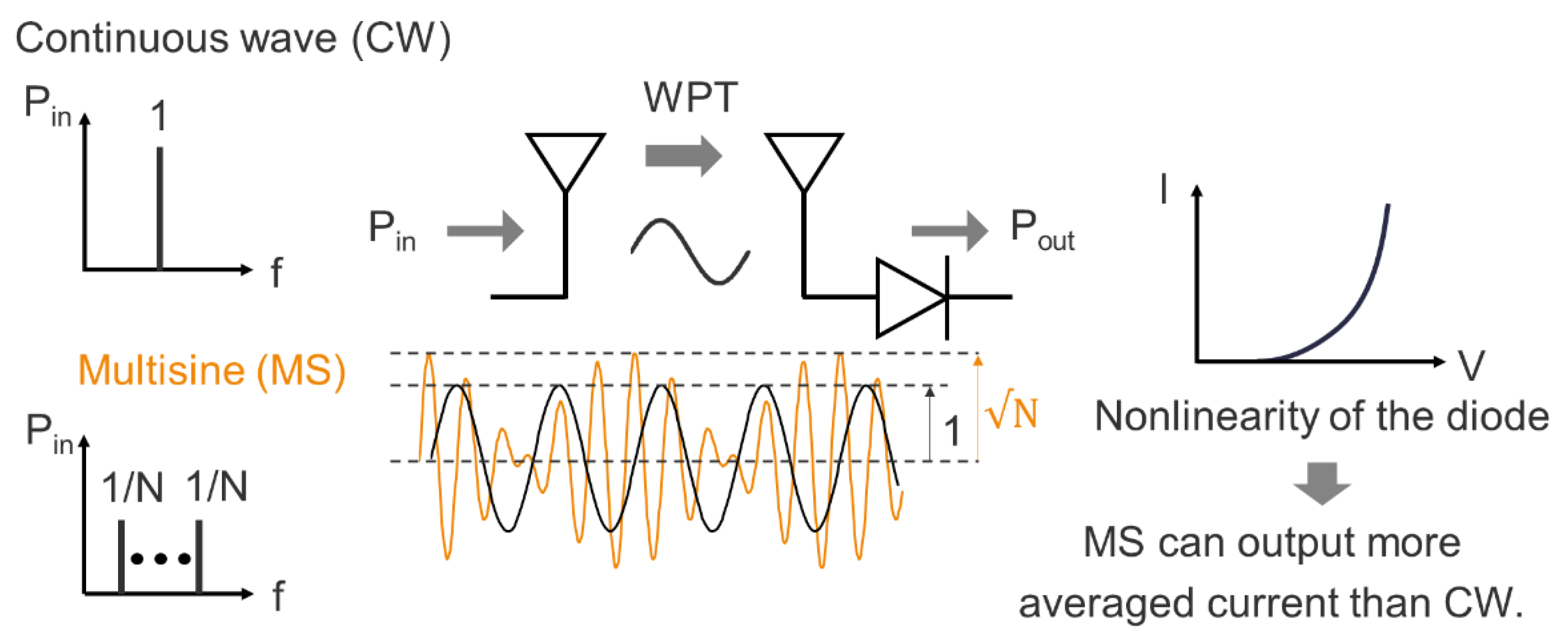
:1. Introduction
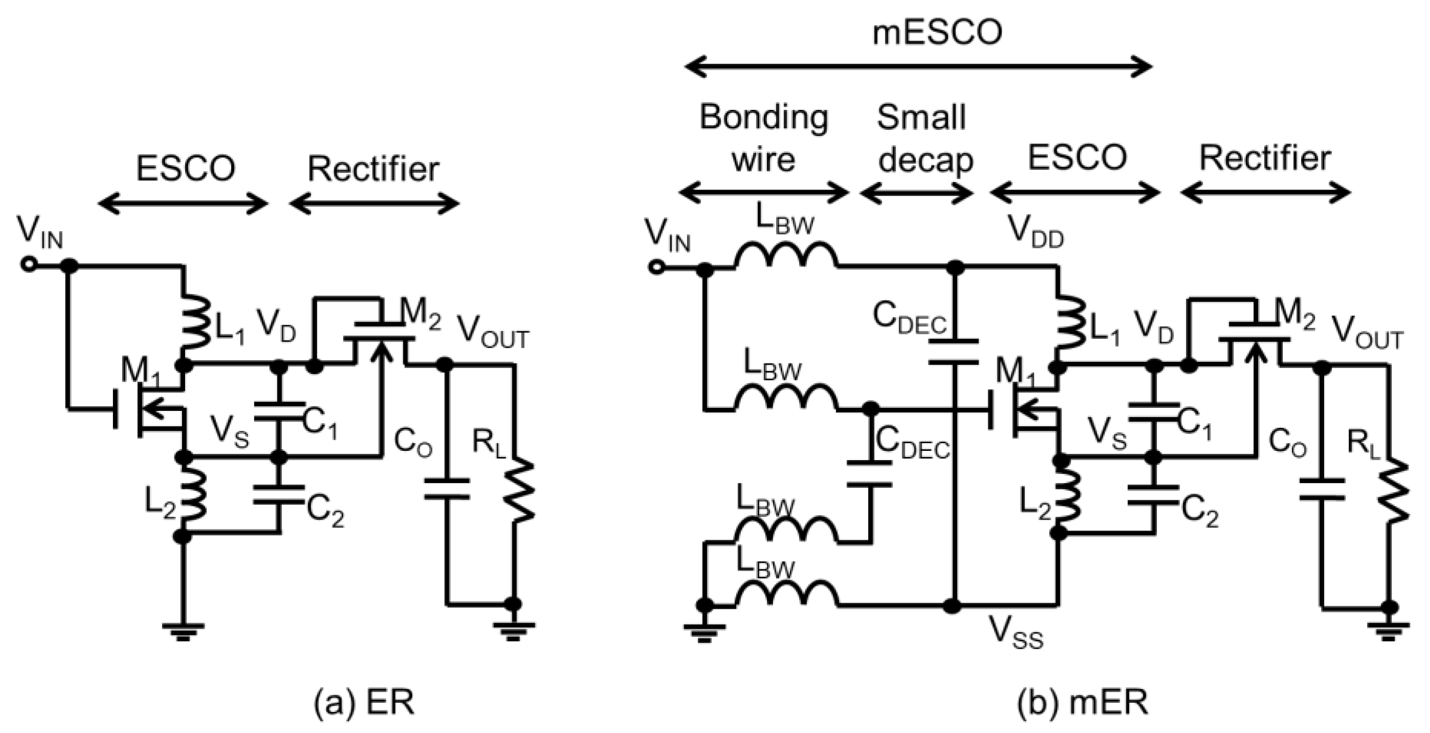
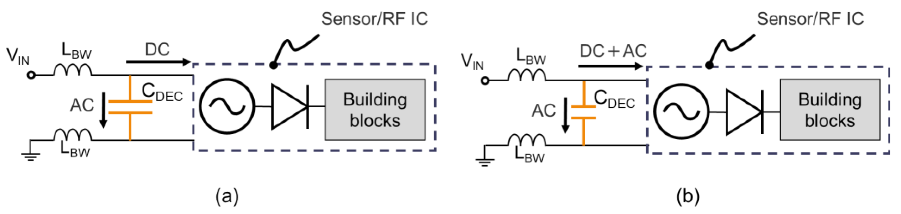
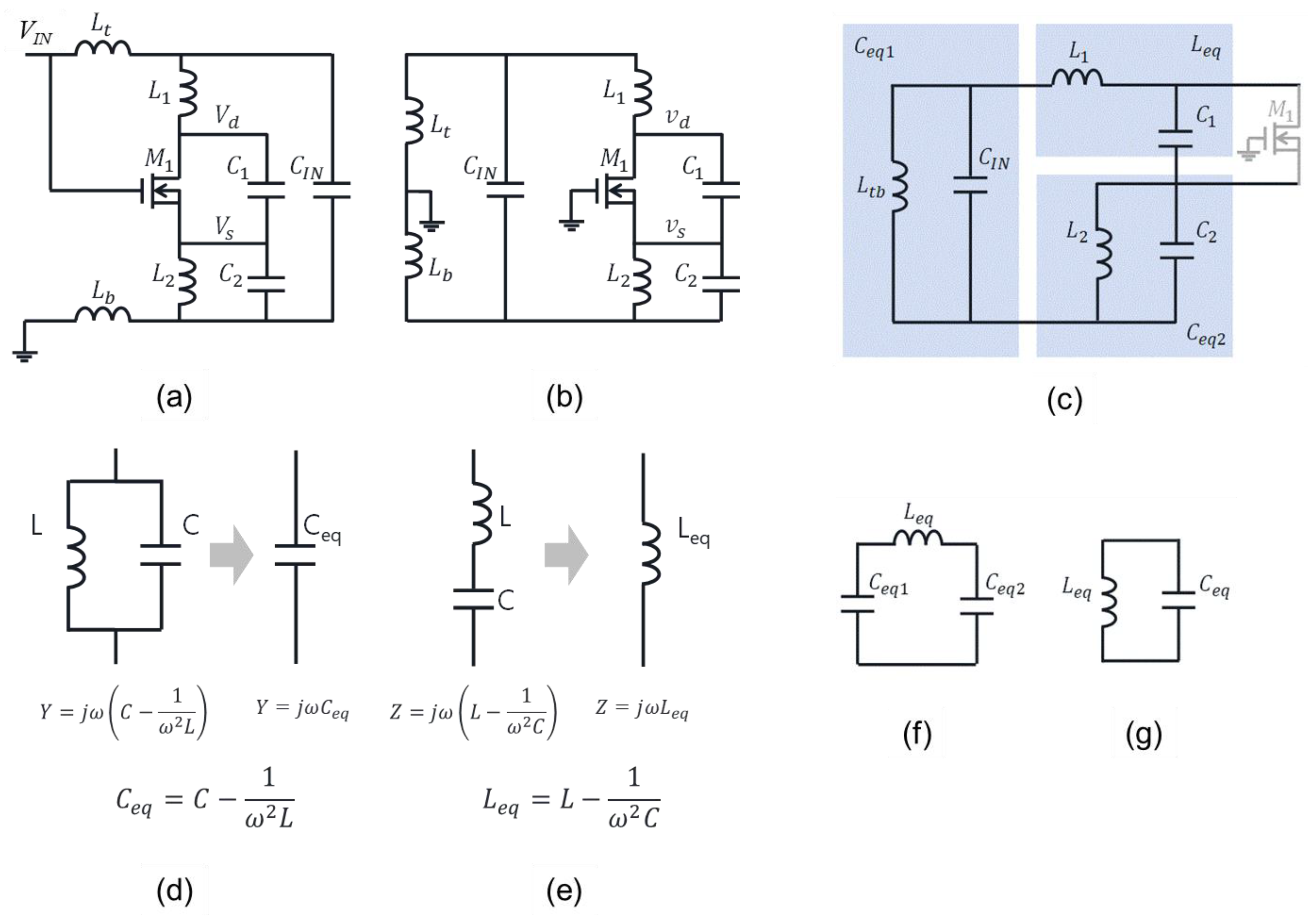
2. More Enhanced Swing Colpitts Oscillator (mESCO), and DC–DC Converter with mESCO and Rectifier (mER)
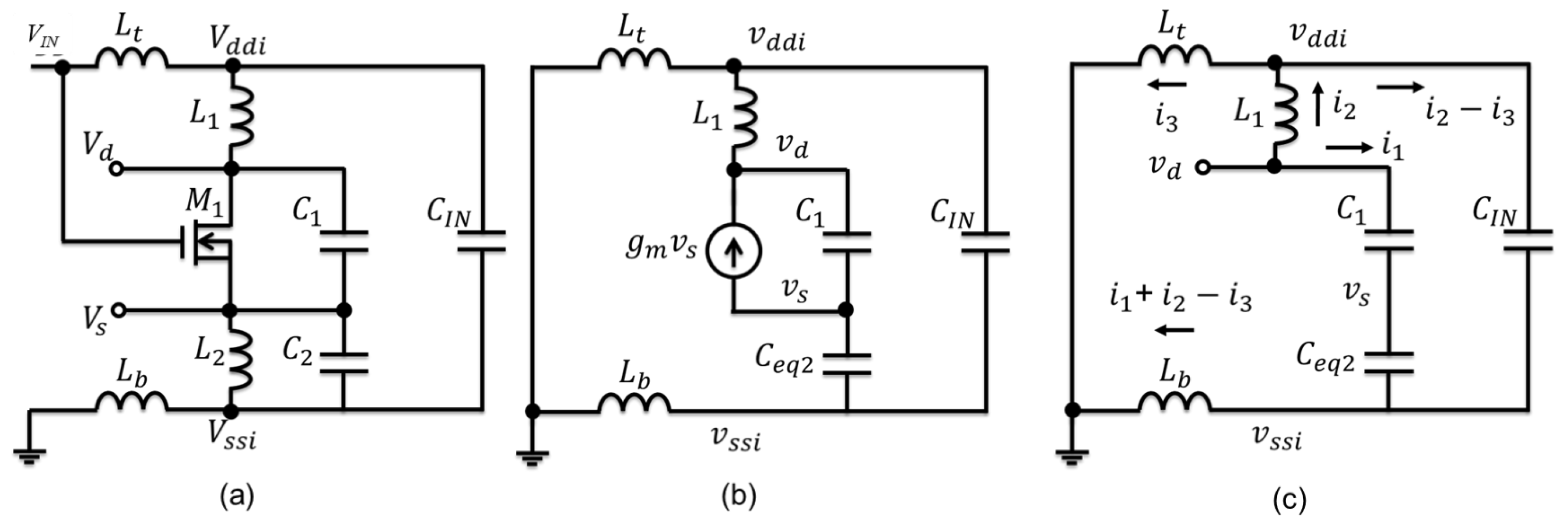
3. Circuit Analysis of mESCO
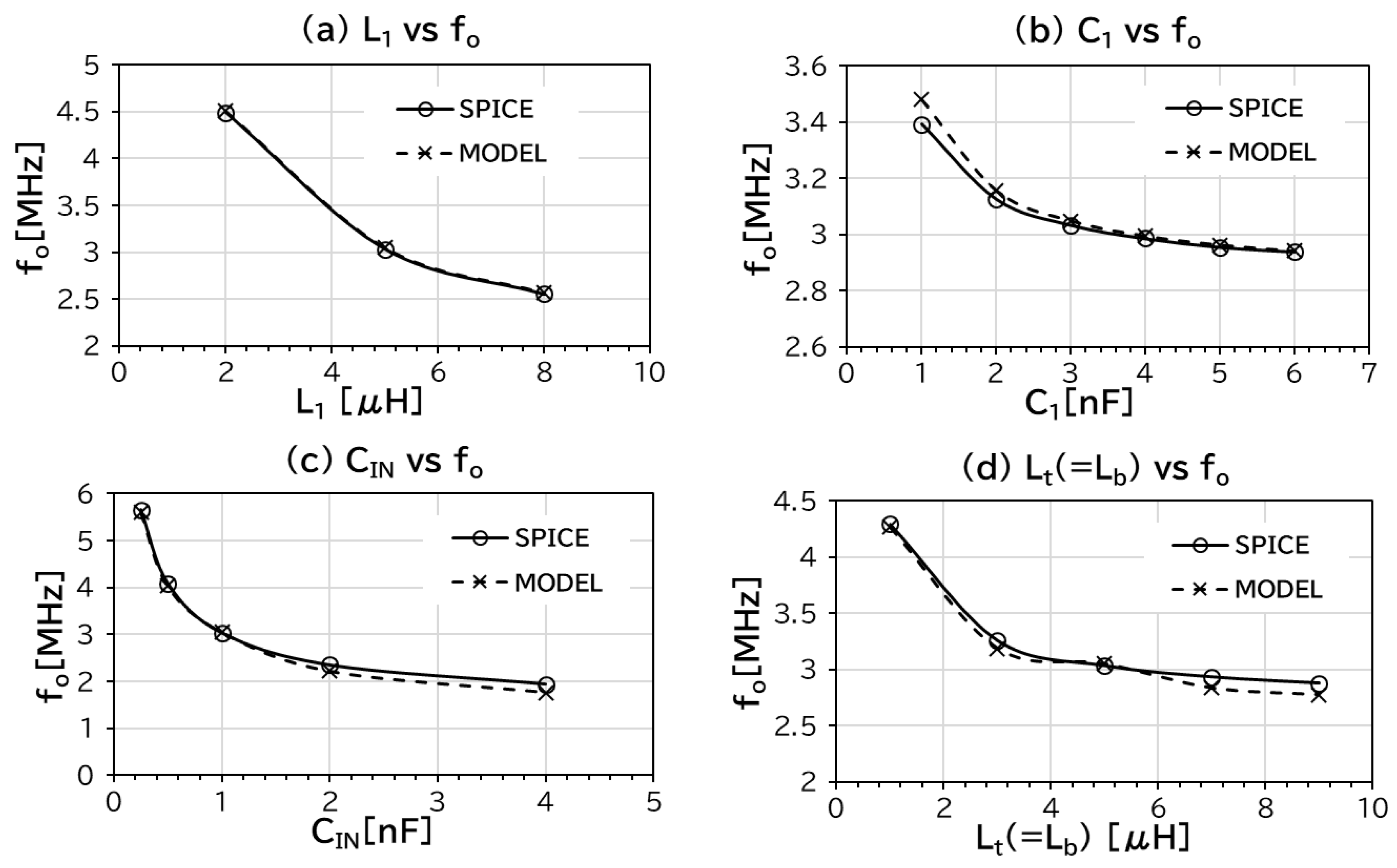
3.1. Oscillation Frequency
3.2. Common-Gate Voltage Gain
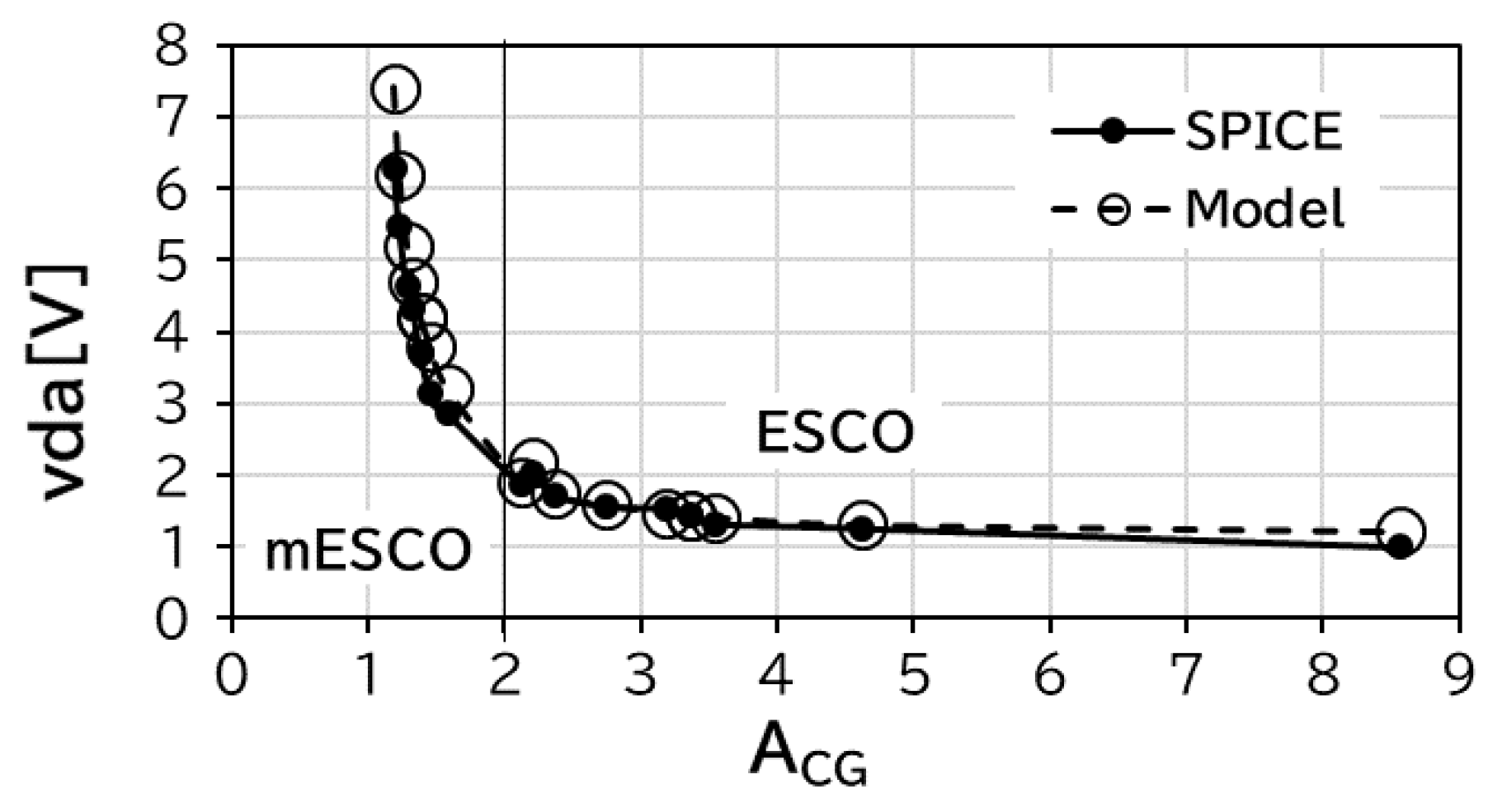
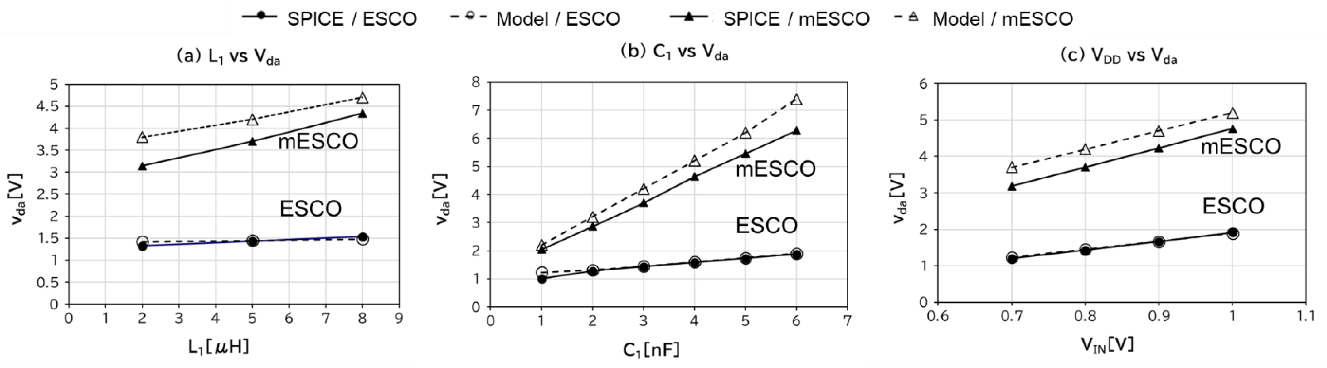
3.3. Drain Voltage Amplitude vda
4. Conclusions
Author Contributions
Funding
Institutional Review Board Statement
Informed Consent Statement
Data Availability Statement
Acknowledgments
Conflicts of Interest
Nomenclature
| ACG | Common gate voltage gain |
| CDEC | Decoupling capacitor |
| ER | ESCO followed by rectifier |
| ESCO | Enhanced swing Colpitts oscillator |
| ET | Energy transducer |
| IoT | Internet of Things |
| LBW | Inductance of bonding wires |
| mER | mESCO followed by Rectifier |
| mESCO | more Enhanced Swing Colpitts Oscillator |
| SPICE | Simulation Program with Integrated Circuit Emphasis |
| vda | Drain voltage amplitude |
| VIN | Input DC voltage |
| VOUT | Output DC voltage |
| VX | DC offset |
| Vx | Voltage difference from ground |
| vx | Voltage difference from the DC offset |
| Vxa | Voltage amplitude |
| WPT | Wireless power transfer |
| θ | Phase |
References
- Shinohara, N. Power without wires. IEEE Microw. Mag. 2011, 12, S64–S73. [Google Scholar] [CrossRef]
- Xie, L.; Shi, Y.; Hou, Y.T.; Lou, A. Wireless power transfer and applications to sensor networks. IEEE Wirel. Commun. 2013, 20, 140–145. [Google Scholar] [CrossRef]
- Amar, A.B.; Kouki, A.B.; Cao, H. Power approaches for implantable medical devices. Sensors 2015, 15, 28889–28914. [Google Scholar] [CrossRef] [PubMed]
- Qian, L.; Cui, K.; Xia, H.; Shao, H.; Wang, J.; Xia, Y. An Inductive Power Transfer System for Powering Wireless Sensor Nodes in Structural Health Monitoring Applications. IEEE Trans. Microw. Theory Tech. 2022, 70, 3732–3740. [Google Scholar] [CrossRef]
- Mitcheson, P.D.; Yeatman, E.M.; Rao, G.K.; Holmes, A.S.; Green, T.C. Energy Harvesting From Human and Machine Motion for Wireless Electronic Devices. Proc. IEEE 2008, 96, 1457–1486. [Google Scholar] [CrossRef]
- Kazmiersuki, T.; Beedy, S. Energy Harvesting Systems: Principles, Modeling and Applications; Springer: Berlin/Heidelberg, Germany, 2010; pp. 1–78. [Google Scholar]
- Trotter, M.S.; Griffin, J.D.; Durgin, G.D. Power-optimized waveforms for improving the range and reliability of RFID systems. In Proceedings of the 2009 IEEE International Conference on RFID, Orlando, FL, USA, 27–28 April 2009; pp. 80–87. [Google Scholar] [CrossRef]
- Boaventura, A.S.; Carvalho, N.B. Maximizing DC power in energy harvesting circuits using multisine excitation. In Proceedings of the 2011 IEEE MTT-S International Microwave Symposium, Baltimore, MD, USA, 5–10 June 2011; pp. 1–4. [Google Scholar] [CrossRef]
- Collado, A.; Georgiadis, A. Optimal Waveforms for Efficient Wireless Power Transmission. IEEE Microw. Wirel. Compon. Lett. 2014, 24, 354–356. [Google Scholar] [CrossRef]
- Clarke, K.K.; Hess, D.T. Communication Circuits: Analysis and Desig; Addison-Wesley Publishing Company: Boston, MA, USA, 1971; Chapter 6. [Google Scholar]
- Zhang, M.; Du, L.; Fang, Z.; Zhao, Z. A sensitivity-enhanced film bulk acoustic resonator gas sensor with an oscillator circuit and its detection application. Micromachines 2017, 8, 25. [Google Scholar] [CrossRef]
- Sharma, S.; Gao, H.; Hueber, G.; Mazzanti, A. A Magnetically Coupled Dual-Core 154-GHz Class-F Oscillator with -177.1 FoM and -87 dBc/Hz PN at 1-MHz Offset in a 22-nm FDSOI with Third-Harmonic Extraction. In Proceedings of the 2022 IEEE Symposium on VLSI Technology and Circuits (VLSI Technology and Circuits), Honolulu, HI, USA, 12–17 June 2022; pp. 12–13. [Google Scholar] [CrossRef]
- Liu, S.-H.; Hung, C.-M.; Chuang, H.-R.; Huang, T.-H. A W-band Push-Push VCO with Gm-Boosted Colpitts Topology in 90-nm CMOS Technology. In Proceedings of the 2021 IEEE International Symposium on Radio-Frequency Integration Technology (RFIT), Hualien, Taiwan, 25–27 August 2021; pp. 1–3. [Google Scholar] [CrossRef]
- Troedsson, N.; Sjoland, H. An ultra low voltage 2.4 GHz CMOS VCO. In Proceedings of the RAWCON 2002 IEEE Radio and Wireless Conference (Cat. No.02EX573), Boston, MA, USA, 11–14 August 2002; pp. 205–208. [Google Scholar] [CrossRef]
- Hsieh, H.; Lu, L. A High-Performance CMOS Voltage-Controlled Oscillator for Ultra-Low-Voltage Operations. IEEE Trans. Microw. Theory Tech. 2007, 55, 467–473. [Google Scholar] [CrossRef]
- Brown, T.W.; Farhabakhshian, F.; Roy, A.G.; Fiez, T.S.; Mayaram, K. A 475 mV, 4.9 GHz Enhanced Swing Differential Colpitts VCO With Phase Noise of -136 dBc/Hz at a 3 MHz Offset Frequency. IEEE J. Solid-State Circuits 2011, 46, 1782–1795. [Google Scholar] [CrossRef]
- Machado, M.B.; Schneider, M.C.; Galup-Montoro, C. On the Minimum Supply Voltage for MOSFET Oscillators. IEEE Trans. Circuits Syst. I Regul. Pap. 2014, 61, 347–357. [Google Scholar] [CrossRef]
- Lim, B.-M.; Seo, J.-I.; Lee, S.-G. A Colpitts Oscillator-Based Self-Starting Boost Converter for Thermoelectric Energy Harvesting With 40-mV Startup Voltage and 75% Maximum Efficiency. IEEE J. Solid-State Circuits 2018, 53, 3293–3302. [Google Scholar] [CrossRef]


| Parameter | Default Value |
|---|---|
| L1 | 5 μH |
| L2 | 16 μH |
| Lt (=Lb) | 5 μH |
| C1 | 3 nF |
| C2 | 8 nF |
| CIN | 1 nF |
| VIN | 0.8 V |
Publisher’s Note: MDPI stays neutral with regard to jurisdictional claims in published maps and institutional affiliations. |
© 2022 by the authors. Licensee MDPI, Basel, Switzerland. This article is an open access article distributed under the terms and conditions of the Creative Commons Attribution (CC BY) license (https://creativecommons.org/licenses/by/4.0/).
Share and Cite
Nomura, T.; Tanzawa, T. More Enhanced Swing Colpitts Oscillators: A Circuit Analysis. Electronics 2022, 11, 2808. https://doi.org/10.3390/electronics11182808
Nomura T, Tanzawa T. More Enhanced Swing Colpitts Oscillators: A Circuit Analysis. Electronics. 2022; 11(18):2808. https://doi.org/10.3390/electronics11182808
Chicago/Turabian StyleNomura, Tatsuya, and Toru Tanzawa. 2022. "More Enhanced Swing Colpitts Oscillators: A Circuit Analysis" Electronics 11, no. 18: 2808. https://doi.org/10.3390/electronics11182808
APA StyleNomura, T., & Tanzawa, T. (2022). More Enhanced Swing Colpitts Oscillators: A Circuit Analysis. Electronics, 11(18), 2808. https://doi.org/10.3390/electronics11182808