
Influence of Substrate and Gate Insulator on the Thermal Characteristics of β-Ga2O3 Field-Effect Transistors: A Simulation Study


Abstract
:1. Introduction
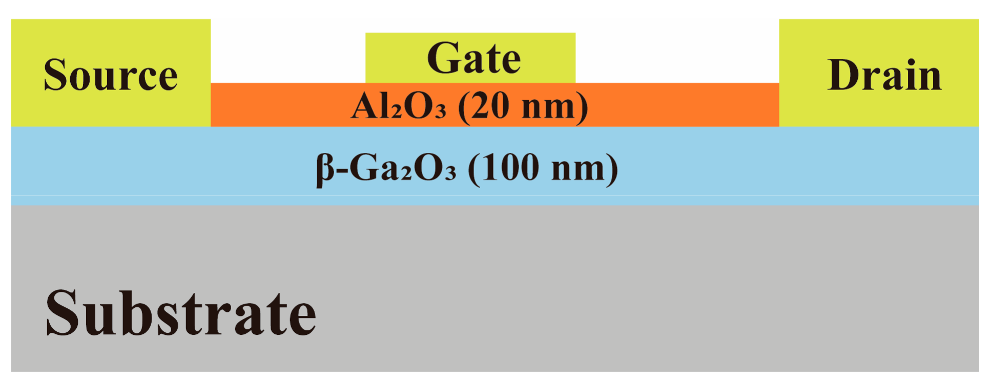
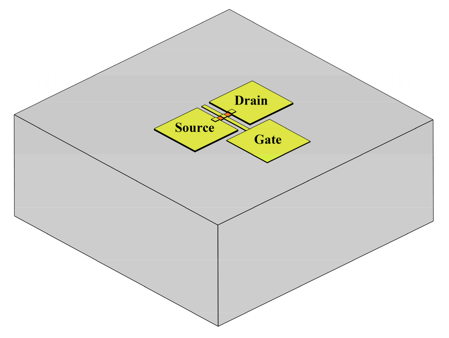
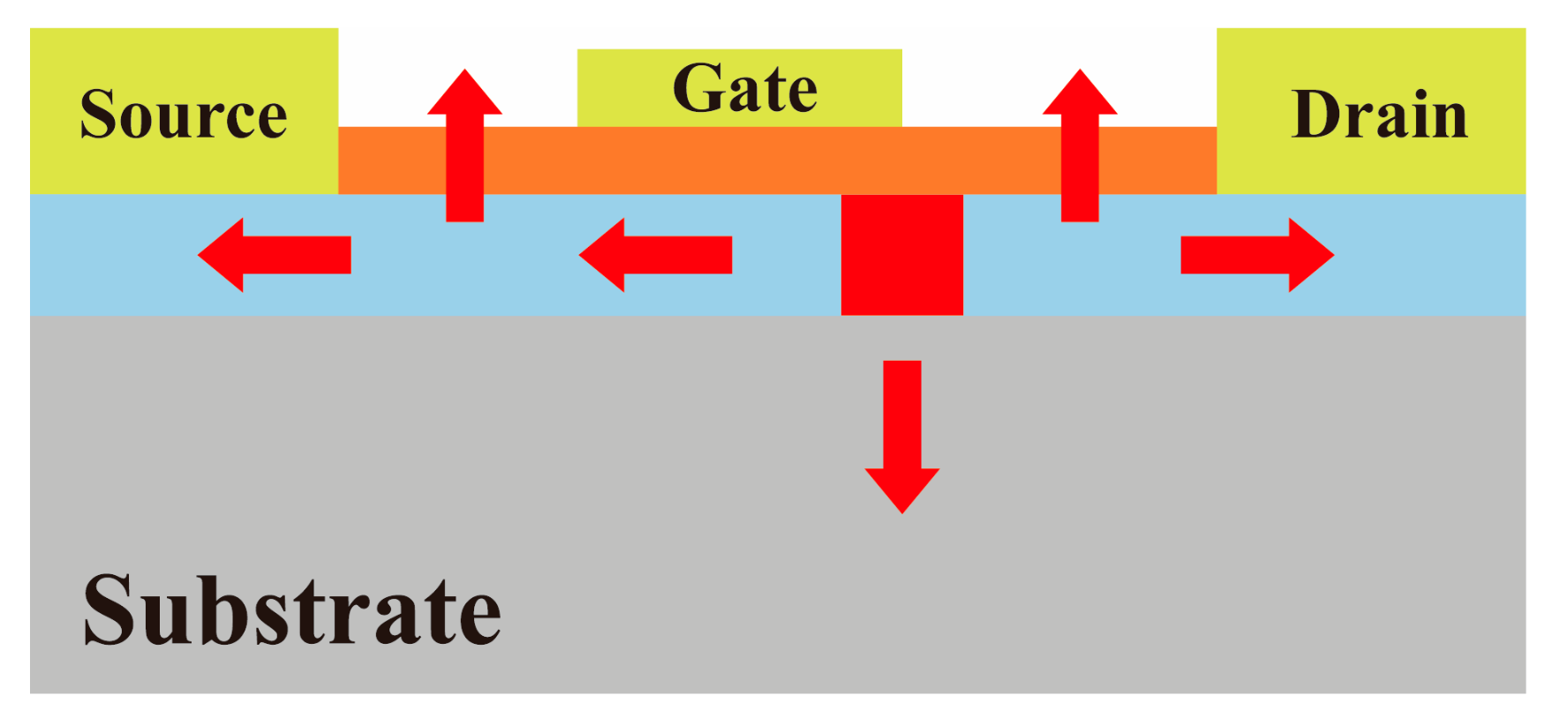
2. Simulation Setup
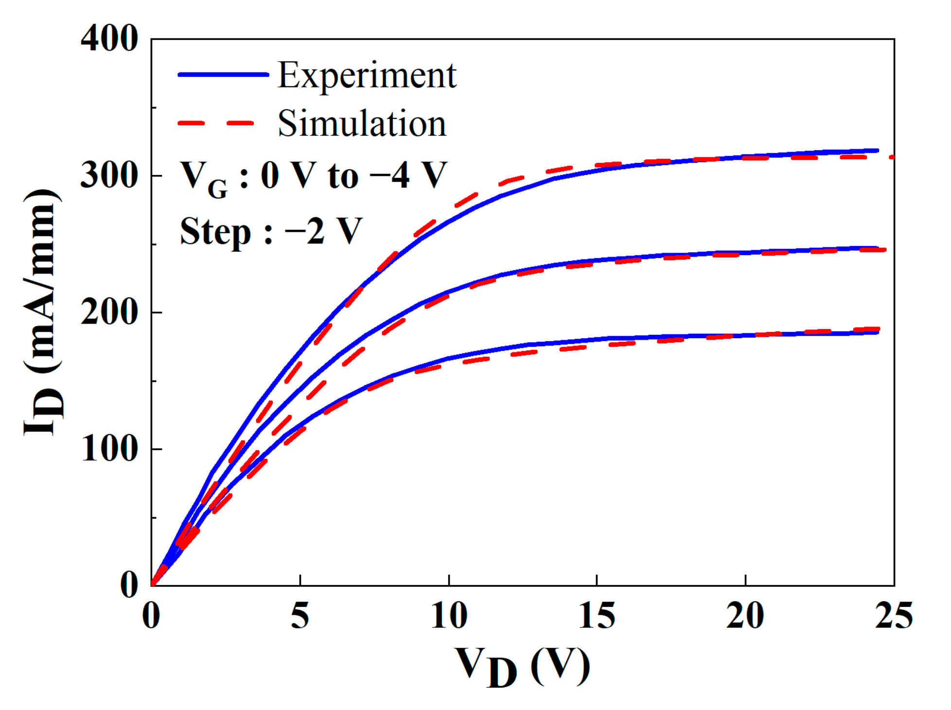
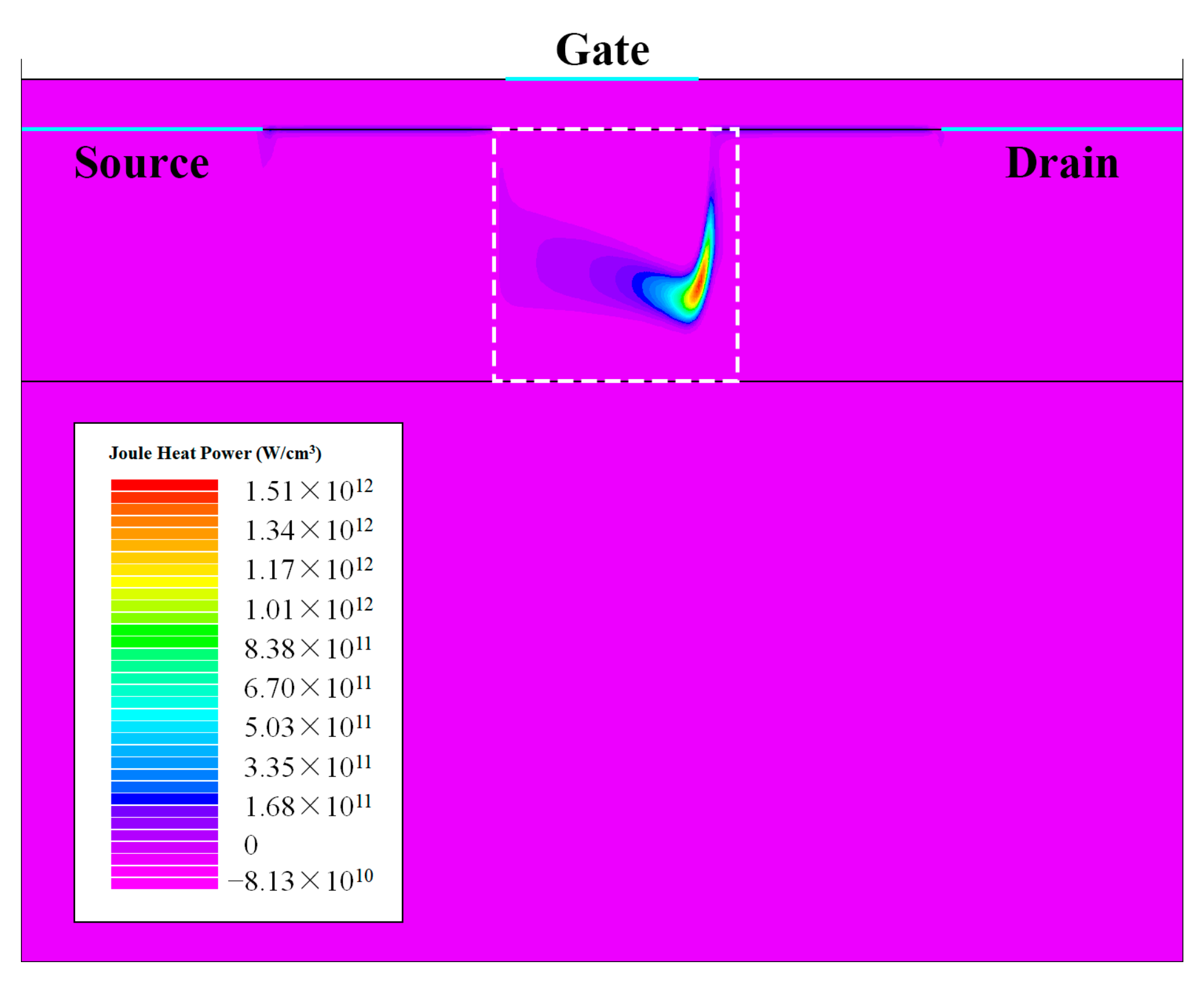
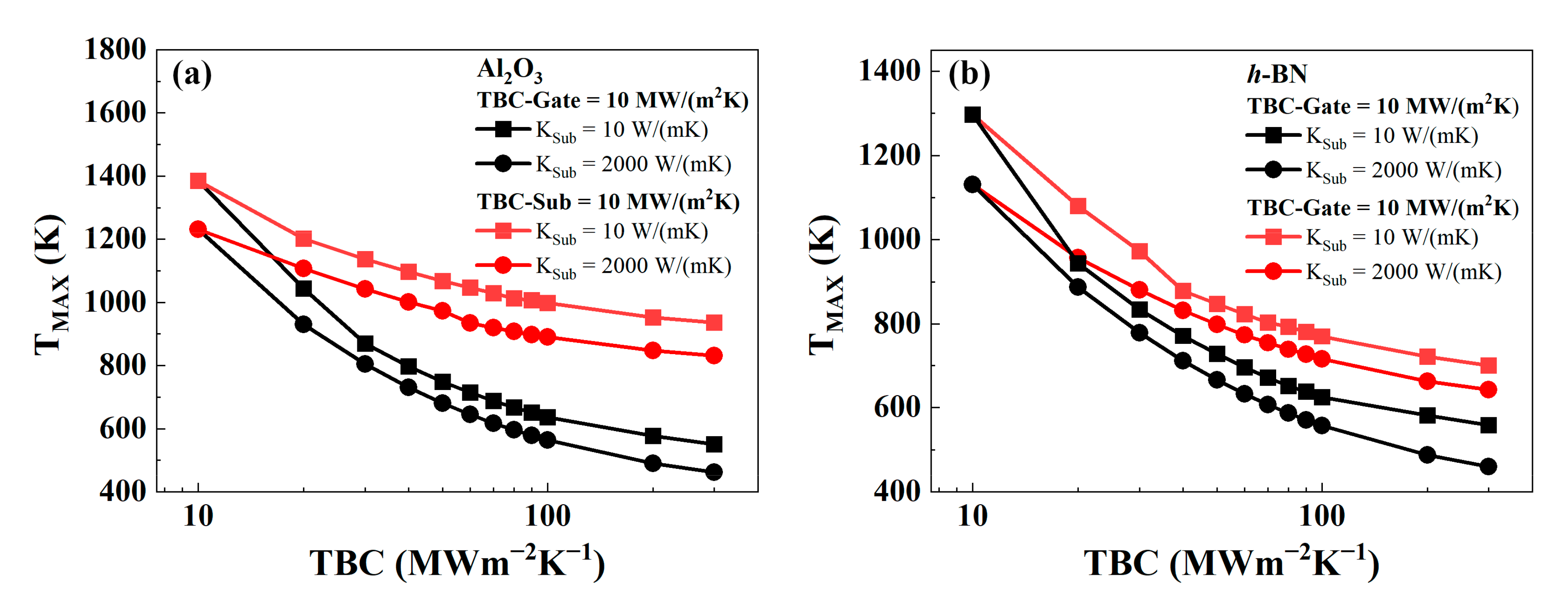
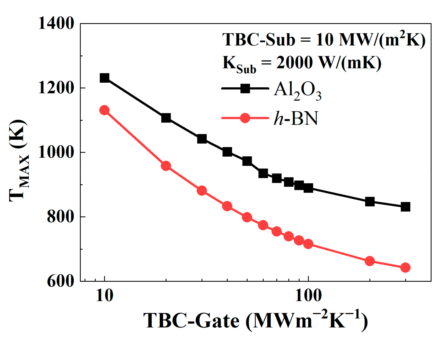
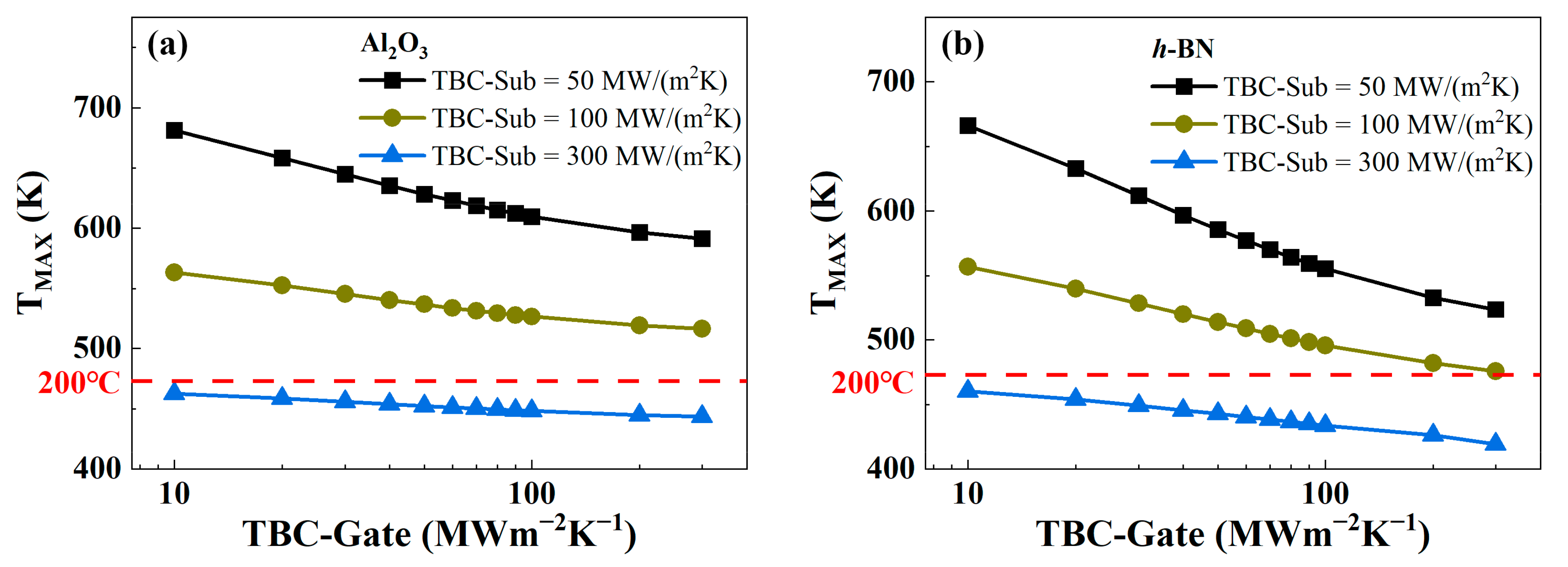
3. Results and Discussion
4. Conclusions
Author Contributions
Funding
Data Availability Statement
Conflicts of Interest
References
- Pearton, S.J.; Yang, J.; Carey, P.; Ren, F.; Kim, J.; Tadjer, M.; Mastro, M.A. A review of Ga2O3 materials, processing, and devices. Appl. Phys. Rev. 2018, 5, 011301. [Google Scholar] [CrossRef] [Green Version]
- Green, A.J.; Chabak, K.D.; Heller, E.R.; Fitch, R.C.; Baldini, M.; Fiedler, A.; Irmscher, K.; Wagner, G.; Galazka, Z.; Tetlak, S.E.; et al. 3.8-MV/cm Breakdown Strength of MOVPE-Grown Sn-Doped β-Ga2O3 MOSFETs. IEEE Electron. Device Lett. 2016, 37, 902–905. [Google Scholar] [CrossRef]
- Mun, J.K.; Cho, K.; Chang, W.; Jung, H.-W.; Do, J. 2.32 kV Breakdown Voltage Lateral β-Ga2O3 MOSFETs with Source-Connected Field Plate. ECS J. Solid State Sci. Technol. 2019, 8, Q3079–Q3082. [Google Scholar] [CrossRef]
- Tadjer, M.J.; Mahadik, N.A.; Wheeler, V.D.; Glaser, E.R.; Ruppalt, L.; Koehler, A.D.; Hobart, K.D.; Eddy, C.R.; Kub, F.J. Communication—A (001) β-Ga2O3 MOSFET with +2.9 V Threshold Voltage and HfO2 Gate Dielectric. ECS J. Solid State Sci. Technol. 2016, 5, P468–P470. [Google Scholar] [CrossRef]
- Xia, Z.; Xue, H.; Joishi, C.; Mcglone, J.; Kalarickal, N.K.; Sohel, S.H.; Brenner, M.; Arehart, A.; Ringel, S.; Lodha, S.; et al. β-Ga2O3 Delta-Doped Field-Effect Transistors With Current Gain Cutoff Frequency of 27 GHz. IEEE Electron. Device Lett. 2019, 40, 1052–1055. [Google Scholar] [CrossRef]
- Lei, D.; Han, K.; Wu, Y.; Liu, Z.; Gong, X. High Performance Ga2O3 Metal-Oxide-Semiconductor Field-Effect Transistors on an AlN/Si Substrate. IEEE J. Electron. Devices Soc. 2019, 7, 596–600. [Google Scholar] [CrossRef]
- Wang, Y.; Xu, W.; Han, G.; You, T.; Mu, F.; Hu, H.; Liu, Y.; Zhang, X.; Huang, H.; Suga, T.; et al. Channel Properties of Ga₂O₃-on-SiC MOSFETs. IEEE Trans. Electron. Devices 2021, 68, 1185–1189. [Google Scholar] [CrossRef]
- Noh, J.; Alajlouni, S.; Tadjer, M.J.; Culbertson, J.C.; Bae, H.; Si, M.; Zhou, H.; Bermel, P.A.; Shakouri, A.; Ye, P.D. High Performance β -Ga2O3 Nano-Membrane Field Effect Transistors on a High Thermal Conductivity Diamond Substrate. IEEE J. Electron. Devices Soc. 2019, 7, 914–918. [Google Scholar] [CrossRef]
- Chatterjee, B.; Zeng, K.; Nordquist, C.D.; Singisetti, U.; Choi, S. Device-Level Thermal Management of Gallium Oxide Field-Effect Transistors. IEEE Trans. Compon. Packag. Manuf. Technol. 2019, 9, 2352–2365. [Google Scholar] [CrossRef]
- Yuan, C.; Zhang, Y.; Montgomery, R.; Kim, S.; Shi, J.; Mauze, A.; Itoh, T.; Speck, J.S.; Graham, S. Modeling and analysis for thermal management in gallium oxide field-effect transistors. J. Appl. Phys. 2020, 127, 154502. [Google Scholar] [CrossRef] [Green Version]
- Ghosh, K.; Singisetti, U. Ab initio velocity-field curves in monoclinic β-Ga2O3. J. Appl. Phys. 2017, 122, 035702. [Google Scholar] [CrossRef] [Green Version]
- Cappella, A.; Battaglia, J.-L.; Schick, V.; Kusiak, A.; Lamperti, A.; Wiemer, C.; Hay, B. High Temperature Thermal Conductivity of Amorphous Al2O3 Thin Films Grown by Low Temperature ALD. Adv. Eng. Mater. 2013, 15, 1046–1050. [Google Scholar] [CrossRef]
- Guo, Z.; Verma, A.; Wu, X.; Sun, F.; Hickman, A.; Masui, T.; Kuramata, A.; Higashiwaki, M.; Jena, D.; Luo, T. Anisotropic thermal conductivity in single crystal β-gallium oxide. Appl. Phys. Lett. 2015, 106, 111909. [Google Scholar] [CrossRef]
- Yamada, T.; Yabutani, H.; Saito, T.; Yang, C.Y. Temperature dependence of carbon nanofiber resistance. Nanotechnology 2010, 21, 265707. [Google Scholar] [CrossRef] [PubMed]
- Alam, M.T.; Bresnehan, M.S.; Robinson, J.A.; Haque, M.A. Thermal conductivity of ultra-thin chemical vapor deposited hexagonal boron nitride films. Appl. Phys. Lett. 2014, 104, 013113. [Google Scholar] [CrossRef]
- Cheng, Z.; Wheeler, V.D.; Bai, T.; Shi, J.; Tadjer, M.J.; Feygelson, T.; Hobart, K.D.; Goorsky, M.S.; Graham, S. Integration of polycrystalline Ga2O3 on diamond for thermal management. Appl. Phys. Lett. 2020, 116, 062105. [Google Scholar] [CrossRef] [Green Version]


| Parameter | Value |
|---|---|
| Bandgap (eV) | 4.8 |
| Relative dielectric constant | 10 |
| Electron effective mass | 0.28 m0 |
| Electron affinity (eV) | 4.0 |
| Conduction band density (cm−3) | 3.6 × 10¹⁸ |
| Valence band density (cm−3) | 2.86 × 10²⁰ |
| Saturated electron velocity (cm/s) | 1.0 × 10⁷ |
| Thermal conductivity | Anisotropy [13] |
| Parameter | Range |
|---|---|
| KSub (Wm−1K−1) | 10–3000 |
| Gate Insulator Thermal Conductivity | Al2O3 or h-BN |
| TBC-Sub (MWm−2K−1) | 10–300 |
| TBC-Gate ((MWm−2K−1)) | 10–300 |
Publisher’s Note: MDPI stays neutral with regard to jurisdictional claims in published maps and institutional affiliations. |
© 2022 by the authors. Licensee MDPI, Basel, Switzerland. This article is an open access article distributed under the terms and conditions of the Creative Commons Attribution (CC BY) license (https://creativecommons.org/licenses/by/4.0/).
Share and Cite
Liu, C.; He, H.; Zhou, X.; Liu, W. Influence of Substrate and Gate Insulator on the Thermal Characteristics of β-Ga2O3 Field-Effect Transistors: A Simulation Study. Electronics 2022, 11, 2323. https://doi.org/10.3390/electronics11152323
Liu C, He H, Zhou X, Liu W. Influence of Substrate and Gate Insulator on the Thermal Characteristics of β-Ga2O3 Field-Effect Transistors: A Simulation Study. Electronics. 2022; 11(15):2323. https://doi.org/10.3390/electronics11152323
Chicago/Turabian StyleLiu, Chaochao, Hao He, Xinlong Zhou, and Wenjun Liu. 2022. "Influence of Substrate and Gate Insulator on the Thermal Characteristics of β-Ga2O3 Field-Effect Transistors: A Simulation Study" Electronics 11, no. 15: 2323. https://doi.org/10.3390/electronics11152323
APA StyleLiu, C., He, H., Zhou, X., & Liu, W. (2022). Influence of Substrate and Gate Insulator on the Thermal Characteristics of β-Ga2O3 Field-Effect Transistors: A Simulation Study. Electronics, 11(15), 2323. https://doi.org/10.3390/electronics11152323