Abstract
A low insertion loss, wideband 6-bit digital step attenuator is implemented in the 0.25-μm GaAs pHEMT process. Modified π- or T-type attenuator structures are adopted to expand the operation frequency bandwidth and reduce the insertion phase violation. Furthermore, the through-wafer via (TWV) is analyzed to reduce the influence of the parasitic effect on the high-frequency performance of the attenuator. The depletion mode single-gate switch transistors are used to control the on-off state of the attenuator, which provides low insertion loss and high isolation. The step of the attenuator is 0.5 dB, and the attenuation range is 31.5 dB. The measurement results show a maximum root mean square (RMS) attenuation error of 0.51 dB and RMS phase error of 6.6 degrees from DC-18 GHz. The chip area is 1.8 × 0.6 mm2.
1. Introduction
The attenuator is one of the key devices in phased array systems, which is mainly used for amplitude adjustment and damage protection [1]. The digital step attenuator (DSA) using π- or T-type units has the advantages of a wideband, high precision, high linearity, being bidirectional, and a small amplitude error [2,3]. In recent years, several technologies have been used in wideband DSA aimed at reducing the phase error and increasing the working bandwidth [4,5,6,7,8,9]. The internal switched π- or T-type attenuator with passive compensation components is popular for compact chip sizes. The passive components are added into the π- or T-type structure to form low-pass characteristics in both the reference and attenuation states. Therefore, the phase–frequency curves of the two states decrease similarly with the increase in the frequency, and the phase difference is reduced.
However, the performance of the low-pass network adopted in the π- or T-type attenuators is always influenced by the parasitic component of the passive devices. The low Q factor inductance would induce additional insertion loss, and it would also be limited by the operating frequency. A good solution to avoid using inductance is to assign the capacitors in parallel with the shunt resistors of the π- or T-type attenuator [7]. The bypass compensation capacitors play the role of low-pass components, and they also expand the operation frequency. Unfortunately, when using relatively large transistors as series switches, the bypass compensation capacitors would cause attenuation degradation at high frequencies when needing a large value to reduce the phase error. In addition, a larger capacitance in the shunt branches will also increase the insertion loss at high frequencies.
Compared with the CMOS process, attenuators based on the gallium arsenide (GaAs) process have low insertion loss at high frequencies [10]. However, the performance at high frequencies will also be affected by the parasitic components. It is still difficult to reduce the attenuation and phase errors at the same time, even if compensation capacitances are adopted. The size of pHEMT is not as flexible as MOSFET, which leads to many difficulties in balancing the attenuation and phase error.
In this paper, a wideband digital step attenuator is implemented in 0.25-μm GaAs pHEMT technology. A modified π-type attenuator structure with additional compensation capacitance is adopted. The middle capacitance between the shunt branch of the π-type attenuator adds a new degree of freedom in optimizing the phase and attenuation error. The parasitic effect of through-wafer via (TWV) is also analyzed and optimized to improve the performance. The implementation of the circuit is introduced in Section 2. The fabrication and measurement results are shown in Section 3. Finally, Section 4 concludes the performance of the attenuator.
2. Implementation of the Attenuator Circuit
Figure 1 is the diagram of the proposed attenuator circuit, which combines six π- or T-type attenuation units in cascade. To minimize the chip size and keep good matching and attenuation performance, different types of attenuation units are used to implement various values, and inter-stage inductances are added to the large value attenuator cells. The small attenuation elements adopt a reduced T-type structure, while the medium elements adopt a bridged T-type structure and the larger cells, such as those of 8 dB and 16 dB, adopt a π-type structure.
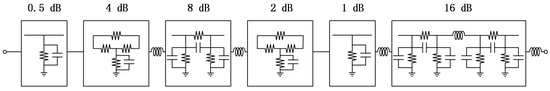
Figure 1.
The diagram of the proposed attenuator circuit with the switches neglected.
T-type, bridged T-type, and π-type attenuators can achieve better matching and attenuation performance. To avoid the use of an extreme resistance value, the bridged T-type attenuator is used to achieve 2-dB and 4-dB attenuation units, while the π-type one is used for 8 dB and 16 dB, of which 16 dB is achieved by 2 8-dB units in cascade.
In addition, to reduce the insertion phase shift between the reference and the attenuation states, bypass capacitors are paralleled with the resistors in the shunt branches of the bridged T-type, π-type, and reduced T-type structures, which are shown in Figure 2a–c. The bypass capacitors will change the attenuator into low-pass characteristics in both the reference and attenuation states, which leads to similar phase curves. The phase error is reduced, and the operating bandwidth is also expanded [7].
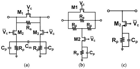
Figure 2.
(a) The modified π-type for the large value attenuator. (b) The modified bridged T-type for the middle value attenuator. (c) The modified reduced T-type attenuator for the small value attenuator.
For large value attenuation units with a π-type structure, the phase difference is relatively high, which requires a larger value capacitor for compensation. However, the introduced bypass capacitor will increase the transmission loss at high frequencies, and the attenuation curve thus deteriorates. To alleviate this problem and further increase the working bandwidth of the attenuator, a compensation capacitor Cm in the middle of the parallel branch is introduced. The capacitor Cm can adjust the transmission curve of the attenuation state, and it hardly affects the reference state. By using the capacitor flexibly, both the attenuation and phase error of the attenuator can be minimized. Aside from the bypass capacitor, this can lead to gaining an extra degree of freedom in designing the attenuator [9]. The capacitor Cm actually adjusts the locations of the zeros and poles in the attenuation state. A larger Cm will decrease the phase difference and the attenuation in the middle frequency of the attenuator. Compared with simply increasing Cp, the phase difference is reduced at the cost of continuously increasing the high-frequency attenuation. The additional Cm capacitance allows for more freedom in the attenuator’s design.
All the circuits are grounded to the bottom metal plane of the chip by a through wafer via (TWV). The TWV also has a great influence on the high-frequency response of the attenuator. It can be modeled as shown by the equivalent circuit in Figure 3. The inductor Lp and resistor Rp are used to model the reactive and inactive behavior of the main body of the TWV. The resistor Rsub and capacitor Csub are implemented to account for the parasitic effect of the substrate. Small inductors Ls act as the inductive part of the top metal pad. The TWV is simulated by electromagnetic (EM) simulation tool, and the S-parameter file is extracted. All the parameters are optimized to make the model closed to the simulation results.
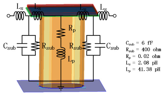
Figure 3.
The equivalent circuit of the TWV.
The shunt branches of the attenuators are grounded by TWVs, so the attenuators are not grounded ideally. Additional parasitic components would worsen the performance at high frequencies, especially in large attenuation units. To reduce the influence of the TWV on the attenuator, multiple TWVs are connected in parallel by the underlying metal layer. The number of the paralleled TWVs is optimized to satisfy the performance and chip size. It can be seen in Figure 4 that the attenuation curve of the 8-dB attenuator with two TWVs in parallel decreases first and then increases, being much flatter than that with just one TWV. At the same time, the phase difference is adjusted to a small value at high frequencies. Similarly, the 16-dB attenuator cells consist of two 8-dB cells, and all four TWVs are connected in parallel.
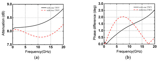
Figure 4.
(a) The attenuation and (b) phase difference of the 8-dB cells with one and two TWVs.
3. Fabrication and Measurement Results
The proposed attenuator circuit was fabricated by a GaAs 0.25-μm pHEMT process. The chip photo is shown in Figure 5, and the size was 1.8 × 0.6 mm2 including the pads. The 6-bit attenuator was controlled by voltages of 0 or −5 V. The switch pHEMTs had gates with a 0.5-μm gate length in this work, and the widths were in different series and parallel branches. Except for the reduced T-structure attenuator, the control voltages of the series and parallel transistors were logically opposite, with 0 V for on and −5 V for off. The input and output ports were ground-signal-ground (GSG) pads, and both ground pads were grounded by TWVs. The chip was fixed to the ground plane of the PCB using conductive silver glue, and all the control pads were bonded to the PCB by gold wire. The DC to DC chip provides −5V negative voltage, and multiple switches control the corresponding logical voltage in the control PCB. The diagram of the measurement setup is shown in Figure 6, including network analyzer, DC power, RF probe station, measurement PCB, device under test (DUT) and control PCB.
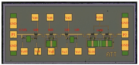
Figure 5.
Photo of the proposed attenuator.
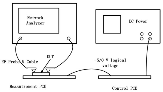
Figure 6.
The diagram of the measurement setup.
The chip was measured on-chip with a microwave probe station and Keysight N5247B network analyzer. The measured transmission curves of all attenuation states are shown in Figure 7, and the insertion loss of the reference state was 2.6~3.6 dB. The attenuation and relative phase differences of the main states are shown in Figure 8. The reflection coefficients of both the input and output ports were less than −11 dB, as shown in Figure 9. The root mean square (RMS) errors of the attenuation and insertion phase shift are shown in Figure 10, where the RMS error of attenuation was less than 0.51 dB and the RMS error of the insertion phase shift was less than 6.6 degrees. A comparison between the attenuators of different technologies and topologies is shown in Table 1. The work had good insertion loss performance compared with the CMOS process and relatively low phase and attenuation errors in such a frequency bandwidth.
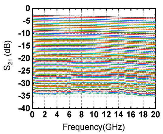
Figure 7.
Measurement results of the S21 in all states.
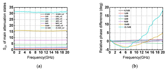
Figure 8.
(a) Measurement results of the S21 in the main states. (b) The relative phase difference curve of the main states.
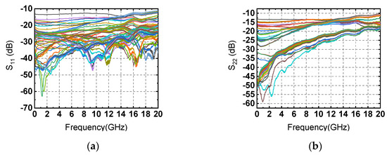
Figure 9.
(a) Measurement results of the S11 and (b) S22.
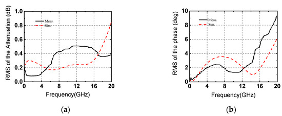
Figure 10.
(a) Measurement and simulation results of the attenuation RMS error. (b) RMS error of the insertion phase shift.

Table 1.
Performance comparison of the attenuator circuits.
4. Conclusions
This paper proposed a wideband, low phase variation 6-bit step attenuator. Modified reduced T-type, bridged T-type, and π-type attenuators were used to implement attenuators of the corresponding values. The pHEMTs act as switches and offer low insertion loss and good isolation. By adding different compensation capacitances properly, the phase difference between states was lower, and the bandwidth was expanded. The parasitic effect of the TWV was alleviated by having several in parallel. The attenuator had a low insertion loss of 2.6~3.7 dB, and the attenuation range was 31.5 dB with a step of 0.5 dB. The attenuation RMS error was less than 0.51 dB, and the phase RMS error was less than 6.6 degrees. Considering the inaccuracy of the process model, there was a certain deviation between the simulation results and the test results, but this paper still provides some attempts to improve the working bandwidth and phase error of the attenuator.
Author Contributions
Conceptualization, D.H. and W.Z.; methodology, D.H. and X.L.; software, D.H. and X.L.; validation, D.H. and Y.L.; formal analysis, D.H.; investigation, D.H.; resources, D.H. and W.Z.; data curation, Y.L.; writing—original draft preparation, D.H.; writing—review and editing, Y.L.; visualization, D.H.; supervision, W.Z.; project administration, W.Z.; funding acquisition, W.Z. All authors have read and agreed to the published version of the manuscript.
Funding
This research received no external funding.
Institutional Review Board Statement
Not applicable.
Informed Consent Statement
Not applicable.
Data Availability Statement
Not applicable.
Conflicts of Interest
The authors declare no conflict of interest.
References
- Dogan, H.; Meyer, R.G. Intermodulation Distortion in CMOS Attenuators and Switches. IEEE J. Solid-State Circuits 2007, 42, 529–539. [Google Scholar] [CrossRef]
- Bae, J.; Lee, J.; Nguyen, C. A 10–67-GHz CMOS Dual-Function Switching Attenuator with Improved Flatness and Large Attenuation Range. IEEE Trans. Microw. Theory Tech. 2013, 61, 4118–4129. [Google Scholar] [CrossRef]
- Dogan, H.; Meyer, R.G.; Niknejad, A.M. Analysis and Design of RF CMOS Attenuators. IEEE J. Solid-State Circuits 2008, 43, 2269–2283. [Google Scholar] [CrossRef]
- Ciccognani, W.; Giannini, F.; Limiti, E. Longhi Compensating for Parasitic Phase Shift in Microwave Digitally Controlled Attenuators. Electron. Lett. 2008, 44, 743–744. [Google Scholar] [CrossRef]
- Ku, B.-H.; Hong, S. 6-Bit CMOS Digital Attenuators with Low Phase Variations for X-Band Phased-Array Systems. IEEE Trans. Microw. Theory Tech. 2010, 58, 1651–1663. [Google Scholar]
- Zhang, L.; Zhao, C.; Zhang, X.; Wu, Y.; Kang, K. A CMOS K-Band 6-Bit Attenuator with Low Phase Imbalance for Phased Array Applications. IEEE Access 2017, 5, 19657–19661. [Google Scholar] [CrossRef]
- Song, I.; Cho, M.; Cressler, J.D. Design and Analysis of a Low Loss, Wideband Digital Step Attenuator with Minimized Amplitude and Phase Variations. IEEE J. Solid-State Circuits 2018, 53, 2202–2213. [Google Scholar] [CrossRef]
- Yuan, Y.; Mu, S.-X.; Guo, Y.-X. 6-Bit Step Attenuators for Phased-Array System with Temperature Compensation Technique. IEEE Microw. Wirel. Compon. Lett. 2018, 28, 690–692. [Google Scholar] [CrossRef]
- Hao, D.; Zhang, W.; Liu, X.; Liu, Y. A DC to 25 GHz 6-Bit Digital Attenuator Based on 0.18 Mm SiGe BiCMOS Technology. Int. J. RF Microw. Comput. Aided Eng. 2021, 31, e22730. [Google Scholar] [CrossRef]
- Dai, Y.-S.; Li, P.; Han, Q.-F.; Chen, S.-B.; Chen, X.; Wang, L.-J.; Xu, L.; Chen, R.-Q. Research on a Novel 2~18 GHz PHEMT MMIC Digital Attenuator with Low Insertion Phase Shift. In Proceedings of the 2012 International Conference on Microwave and Millimeter Wave Technology (ICMMT), Shenzhen, China, 5–8 May 2012; Volume 4, pp. 1–4. [Google Scholar]
Publisher’s Note: MDPI stays neutral with regard to jurisdictional claims in published maps and institutional affiliations. |
© 2022 by the authors. Licensee MDPI, Basel, Switzerland. This article is an open access article distributed under the terms and conditions of the Creative Commons Attribution (CC BY) license (https://creativecommons.org/licenses/by/4.0/).