Article

Design Framework for ReRAM-Based DNN Accelerators with Accuracy and Hardware Evaluation

1
Department of Electronic Engineering, Chung Yuan Christian University, Taoyuan 320314, Taiwan
2
Department of Information and Computer Engineering, Chung Yuan Christian University, Taoyuan 320314, Taiwan
*
Author to whom correspondence should be addressed.
Electronics 2022, 11(13), 2107; https://doi.org/10.3390/electronics11132107
Submission received: 31 May 2022 / Revised: 29 June 2022 / Accepted: 4 July 2022 / Published: 5 July 2022
(This article belongs to the Special Issue Advances in Hardware-Software Codesign)

Abstract

:
To achieve faster design closure, there is a need to provide a design framework for the design of ReRAM-based DNN (deep neural network) accelerator at the early design stage. In this paper, we develop a high-level ReRAM-based DNN accelerator design framework. The proposed design framework has the following three features. First, we consider ReRAM’s non-linear properties, including lognormal distribution, leakage current, IR drop, and sneak path. Thus, model accuracy and circuit performance can be accurately evaluated. Second, we use SystemC with TLM modeling method to build our virtual platform. To our knowledge, the proposed design framework is the first behavior-level ReRAM deep learning accelerator simulator that can simulate real hardware behavior. Third, the proposed design framework can evaluate not only model accuracy but also hardware cost. As a result, the proposed design framework can be used for behavior-level design space exploration. In the experiments, we have deployed different DNN models on the virtual platform. Circuit performance can be easily evaluated on the proposed design framework. Furthermore, experiment results also show that the noise effects are different in different ReRAM array architectures. Based on the proposed design framework, we can easily mitigate noise effects by tuning architecture parameters.

1. Introduction

Artificial intelligent has been recognized as a promising solution in many research areas, such as computer vision, medical science, etc. Diverse kinds of DNN (deep neural network) are widely used in classification, object detection, semantic segmentation, and so on. CNN (convolutional neural network) is the most common DNN (deep neural network) to apply in many applications. In the history of CNN, from the Hinton-proposed AlexNet [1], the revolution of neural networks started. VGG [2], ResNet [3], SqueezeNet [4] and DenseNet [5] have been proposed one after another. A CNN is composed of many MVM (matrix vector multiplication) with a large amount of input activations and weight parameters. Additionally, the model size of modern DNN grows dramatically with the progress due to getting deeper. It means the computing of modern models may cause longer latency and larger power consumption. As a result, there is a demand for a highly efficient DNN accelerator to let the model be computed with high performance.
Traditionally, DNN accelerators are based on the von Neumann architecture design concept. Traditional DNN accelerators can be divided into three main branches, namely systolic arrays [6,7,8], reduction trees [9], and network on chip (NoC) [10,11,12]. Although each architecture has its own advantages, their design concepts are based on von Neumann architecture where computations and data storage are separated. They [6,7,8,9,10,11,12] are unable to overcome the bottleneck caused by data movements (owing to the von Neumann architecture). Some previous works [13,14,15] have attempted to reduce this bottleneck using data streams. However, their improvements cannot completely resolve the data movement problem.
In recent years, a rising star called memristor-based DNN accelerators has been proposed [16,17]. Innovations in memristor-based computing systems offer promising solutions for improving the power efficiency of MVM computation. Memristor-based DNN accelerators perform MVM computation with high energy efficiency, which is the most important part of memristor-based neuromorphic computing systems. In these architectures [16,17], the weights are stored in memory and the input activations are converted to an analog signal. Then, the dot product is computed directly in memory. As a result, significant data movements can be saved.
Innovations in memristor-based in-memory computing accelerators provide a promising solution for reducing the required data movements and improving the energy efficiency of DNN computing. Recent work [18] has shown that metal oxide ReRAM (resistive random-access memory) can be used to build crossbar structures to efficiently perform MVM in the convolution and fully connected layers of DNNs. Comparing to CPUs, GPUs or conventional accelerators based on the Von Neumann architecture, ReRAM-based DNN accelerators [16,17] can offer significant power savings since they have the ability to perform arithmetic operations in the data storage.
ReRAM-based DNN accelerators have been proved to be the best solution [19,20]. Note that ReRAM has small Read and Write latency. In addition, ReRAM cells are small and can store multiple levels. While the electrical properties and crossover structures of ReRAM enable energy-efficient DNN computing, the physical properties (non-linear factors) also make ReRAM-based DNN accelerators prone to errors. When performing a MVM computation in a ReRAM crossbar array, multiple word lines are activated simultaneously and the currents flowing through different cells in the same bit line are accumulated to obtain the sum of the products. Even if none of the cells in the same bitline are in error, the result of sum-of-products for the sense amplifier readout may still be incorrect [21], mainly due to the error accumulated from each activate cell in the same bitline and the resolution limited by ADC. Additionally, some previous works [22,23] studied the memory reliability problem. Since many factors affect the reliability of ReRAM-based DNN accelerators, to accurately evaluate DNN model performance at the early design stage, a simulation platform is required to estimate the impact of non-linear factors and hardware limitations on the inference accuracy of the target neural network.
For large-scale applications of ReRAM-based DNN accelerators, several different factors may affect performance. Therefore, an accurate simulation at the early stage is required to estimate and optimize the performance of the design. However, none of the existing simulation platforms fully support accurate error rate analysis and hardware performance evaluation. In previous years, some works have investigated the performance and energy efficiency of ReRAM-based accelerators and proposed simulation tools to facilitate design space exploration [24,25,26,27,28,29]. In [25,26], they only focus on accuracy, but neglect important hardware information. In [24,25,27,29], they use C/C++ programming language to build hardware behavior models and simulate the neural network computing by DNN framework with python wrapper. Since C/C++ are software programming languages, they just can be used to validate the function, but are insufficient for representing actual behavior of hardware circuit. On the other hands, MNSIM [24,28] can both simulate accuracy and report hardware information, but it has a shortage that it does not take memory properties such as leakage current and sneak path into account. Additionally, its hardware information is a behavior-level evaluation that has a lot of errors comparing to the real hardware design. Note that a simulator modeling hardware behavior can just validate the function of the system. In other words, MNSIM [24,28] lacks practical circuit performance evaluation. Therefore, an accurate simulation platform with accuracy and practical hardware evaluation is urgently needed to fully explore the impact of hardware errors and performance on various DNN accelerator architectures.
To overcome the problem that a behavior simulator lacks of hardware circuit performance evaluation, a practical way is to use a high level programming language with hardware properties to model the DNN system. Note that high level programming language can boost the simulation time, while hardware properties can make the simulation result more precise. In recent years, SystemC has been recognized an efficient way is to model a circuit system. SystemC is not only a high-level programming language to allow designers to simulate and maintain efficiently, but it also includes TLM and cycle accurate modeling method to take practical hardware behaviors into account. Note that some research efforts [30] have been devoted to virtual platform of CIM system. In [30], they developed cycle accurate models with non-linear hardware properties considered based on C++ programming language. Their approach [30] has the following two drawbacks. First, cycle accurate modeling method is time consuming. The long time process is inefficient if we only want to get an approximated result such as performance or power consumption for architecture exploration. Second, C++ is not a hardware-oriented programming language. Thus, C++ cannot model a circuit with hardware behavior. Besides, in [31,32], they proposed CIM (computing-in-memories) virtual platforms based on SystemC programming language. However, they [31,32] did not take hardware non-linear effects into account. To accurately evaluate DNN model performance, there is a need to consider the impact of non-linear factors on the target DNN.
From the above observations, we know that there is a demand to provide a design framework that includes a virtual platform with non-linear properties considered based on SystemC. Note that a virtual platform based on SystemC can obtain practical hardware behaviors. A model with the non-linear properties considered can present real properties of memory cells and achieve a precise accuracy on a CIM-based DNN accelerator.
In this paper, we propose a design framework with virtual platform and non-linear properties considered for the development of ReRAM-based DNN accelerators. The proposed design framework includes two parts: software environment and virtual platform (for hardware system). We utilize an open-source compiler TVM to establish our software environment. The compiler optimizes and tiles data dependent on hardware configurations from DNN accelerator. In virtual platform, we use SystemC to build the whole hardware system. We also embed non-linear model into ReRAM cell. Thus, in our work, it can consider not only the accuracy of the software model, but also practical hardware costs, such as latency, area, power consumption and utilization. The proposed design framework can help designers to precisely evaluate the DNN model at the early design stage.
Based on the above observations, in this paper, we propose a simulation framework with virtual platform for the development of ReRAM-based DNN accelerators. The proposed design framework can help designers to precisely evaluate the DNN model at the early design stage. The main contributions of our work are elaborated below.
  • We have integrated RRAM’s non-linear properties, including lognormal distribution, leakage current, IR drop, and sneak path into the proposed design framework. So far, there is no behavior simulator consider these non-linear properties at the same time.
  • We use SystemC with TLM modeling method to build our virtual platform. Thus, our behavior simulator can efficiently simulate hardware performance with real hardware behavior. To our knowledge, the proposed design framework is the first behavior-level ReRAM-based DNN accelerator simulator that can simulate real hardware behavior.
  • The proposed design framework can evaluate not only accuracy, but also hardware cost. Thus, the proposed design framework can be used for the behavior-level design space exploration (e.g., to explore the trade-off between accuracy and hardware cost between with respect to different XBar height/width, bandwidth, etc.)
For the sake of brevity, Table 1 summarizes the comparisons of the proposed design framework with previous works. As shown in Table 1, most prior works focus on the system level simulation. Only [31,32], and the proposed design framework support the virtual platform. Moreover, the proposed design framework is the only one work that considers lognormal distribution, leakage current, IR drop, and sneak path at the same time.

2. Preliminaries

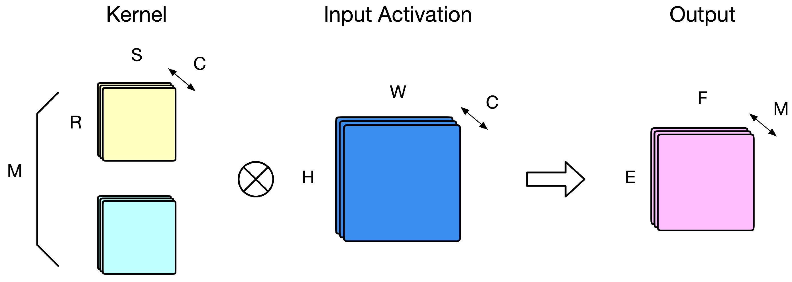
2.1. Convolution Neural Network

Convolution neural network is a widely used technique in computer vision, signal processing, and image processing (such as edge detection and sharpening processing). Apparently, convolution is a critical component in convolution neural network that are used to extract the information of input feature maps. Figure 1 gives an illustration for the two-dimensional (2D) convolution. As shown in Figure 1, a convolution makes several dot products with kernels and input activations. An output will be generated after multiple dot product processing and be transferred as input activations to next layer.
We can simplify dot products to a set of matrix-vector multiplications. Suppose that input activations size has C channels, M amount of R × S kernels and producing output feature map of E × F size with M output channels. The convolution result of output pixel (e,f) in channel m can be expressed as Equation (1):
O u t p u t e , f , m = c = 0 C 1 r = 0 R 1 s = 0 S 1 I n p u t e + r , f + s , c × K e r n e l r , s , c , m
According to the above, the 2D convolution requires intensive data computations and high data throughput. Thus, it is a challenge to design an efficient hardware to process these a lot of MVMs for the 2D convolution. Additionally, it has been recognized that the 2D convolution has a significant impact on the overall performance of a CNN accelerator.

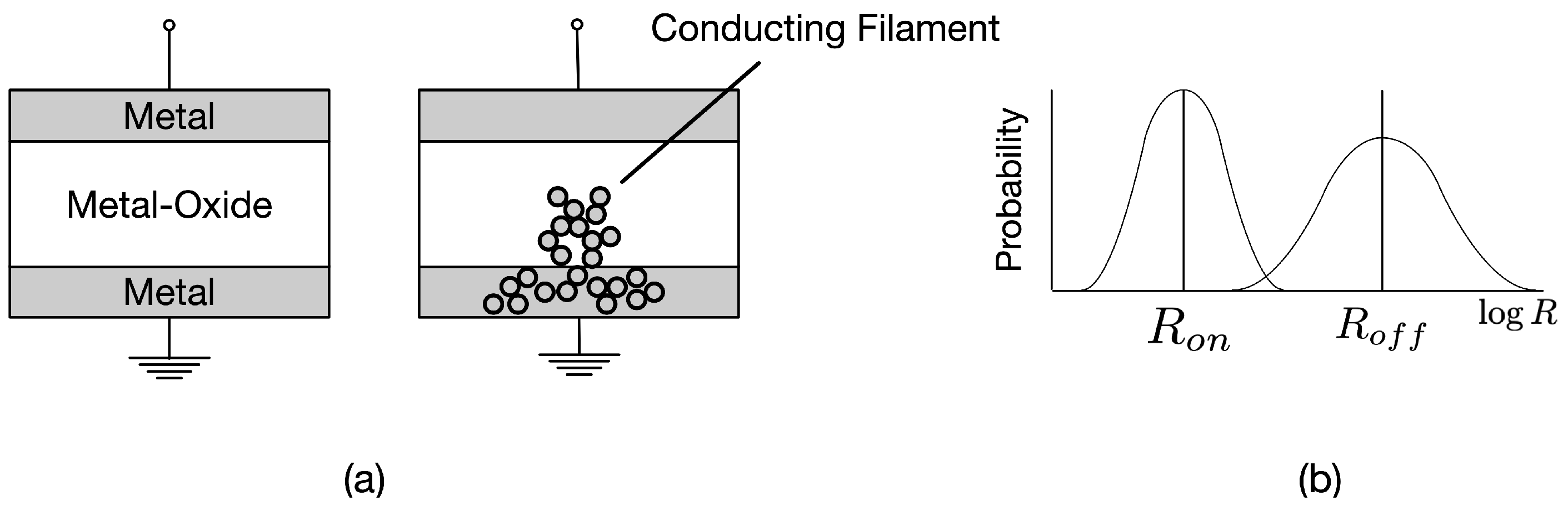
2.2. ReRAM and ReRAM Array

ReRAM has been demonstrated as the best solution for CIMs. It has small read and write latencies. Additionally, its size is small and it can store multiple bits. Here, we use Figure 2 to demonstrate the basic concepts of ReRAM and ReRAM arrays for CIMs. Figure 2a displays one column in a ReRAM array. We store the weight as conductance in ReRAM cells. Inputs are converted to voltage through DAC (digital to analog converter) like Figure 2b. According to Ohm’s law, the computation in a ReRAM cell can be expressed as Equation (2):
I k = G k × V k
where the notation G k is the conductance value (i.e., the reciprocal of resistance R k ), which represents the weight, V k is the voltage, which represents the input value. Thus, current I represents the result of input V multiplies with weight G. Then, the accumulated current of each column in a ReRAM array can be expressed as Equation (3):
I t o t = k I k
where the notation I t o t denotes the accumulated current. In the final, current I t o t will convert to digital through ADC (Analog Digital Converter) as shown in Figure 2b. Note that this function of the column in a ReRAM array can be thought as the behavior of a MAC (multiply- accumulate). In other words, we can treat each column as a MAC. Then, according to this property, we schedule inputs and weights with a suitable dataflow to get the result by CIMs.

2.3. Dataflow of CIM

Because there are lots of computing operations in a convolution, an efficient dataflow is required. Here, we address how to map data to CIM architecture to complete a convolution computation efficiently. For an input feature map, as shown in Figure 1, we need to perform the following convolution computation: input data with dimension H × W × C , kernel with dimension R × S × C × M , and output with dimension E × F × M . Due to the limit of CIM architecture, in general, we store R × S × C to a column and each column store different kernel M, where R represents kernel height, S represents kernel width, C represents channels and M represents different kernels like Figure 3. In a convolution, when weights R × S × C multiply with input activations, they need to be added together. This is the same as the property of CIM architecture in which the current will be accumulated in a column and produce total accumulated current at the bottom of the column as result. Thus, we can also treat a column as a convolution computing of each output pixel. These weights will be stored in the ReRAM memory until all input activations that need to process are completed. Then, the system will store other new weights and do a convolution process again until the whole convolution finishes.

3. Noise Analysis

In this section, we demonstrate non-linear effects of ReRAM DNN accelerator. In Figure 4, we categorize non-linear effects into four kinds (in Figure 4, we use four different colors to represent the four kinds). As shown with red color, there are two non-linear effects (logarithm distribution and leakage current) that occur in a ReRAM cell. As shown with purple color, quantization errors are produced owing to DAC/ADC bit-width. As shown with blue color, wire resistance leads to IR Drop. Finally, as shown with green color, cell properties and array architecture bring out the sneak path. In the following, we discuss and formulate these four kinds of non-linear effects.

3.1. Lognormal Distribution

As shown in Figure 5a, a ReRAM cell is composed with two metal layers and a metal-oxide between them. Once a voltage applies to the upper side of metal layer, it will enable a conducting path in the metal-oxide layer. Since electronics are generated randomly, even we give the same voltage, conducting filament varies each cycle. According to the conductance of ReRAM cell, we can program different state in a ReRAM. As displayed in Figure 5b, the variability of conductance of ReRAM makes the computing result of a ReRAM to have a probability to get an error. This situation gets worse when the number of states of ReRAM gets larger or the result from ReRAM array with lots of uncertain current added together makes ADC hard to convert. Thus, the simulator needs to take this non-linear effect into account to help designers to decide suitable column size and ReRAM state of a ReRAM array. To simply this problem, here we use Gaussian distribution to formulate. The behavior of ReRAM lognormal distribution can be express as Equation (4):
I ( v , g ) = ( I 0 e x p ( g g 0 ) s i n h ( V V 0 ) ) N ( μ , σ 2 )
where I 0 , g 0 and V 0 are fitting parameters from the technology library. Note that the output current I ( v , g ) has a small random deviation due to Gaussian normal distribution. From this formula, we can simulate the practical situation of lognormal distribution in a ReRAM cell.

3.2. Leakage Current

ReRAM cell use conducting filament to conduct memory. In general, A ReRAM cell has at least two states, which are HRS (high resistance state) and LRS (low resistance). HRS represents logic zero and LRS represents logic one. In HRS state, in theory, there is no current passing the ReRAM cell. However, like Figure 6a, in practice, HRS state still has little current. Such a current will be accumulated in a ReRAM array. If the amount of the leakage current (i.e., the current that should not exist) is close to or large than the amount of current from LRS, the output will produce an error. This problem gets worse in two situations: small On/Off ratio and large array size. On/Off ratio is defined as R H R S R L R S . If On/Off ratio is small, the total accumulated leakage current of R H R S in the array can approach R L R S very soon. On the other hand, if the memory size is large, the total leakage current of R H R S is also possibly approaching R L R S . Thus, we should not treat the current in HRS of ReRAM cell as a zero value. The behavior of leakage current can be express as Equation (5):
I t o t = i I L R S , i + H × I L e a k a g e
where I L R S represents the current of each ReRAM cell in LRS state in the column, represents the number of ReRAM cells in the HRS state, and I L e a k a g e represents the leakage current in HRS state.

3.3. Sneak Path

Consider a HRS ReRAM cell is in read mode and all other cells around it are in LRS state. Since HRS has a high resistance, the current from around LRS cells will branch a little to the HRS cell. Thus, as shown in Figure 6b, the current of the HRS cell is larger than expected. Sneak Path has a high relationship with IR drop, since IR drop is also caused by the connected wires between ReRAM cells. The occurrence of sneak path depends on input data and weights stored in the ReRAM. We can avoid the sneak path by changing the dataflow of DNN computation. In our simulator, we take the sneak path effect into account.

3.4. IR Drop

IR drop is also an import factor that causes non-linear properties. This effect is caused by wire resistance, which is another dominant factor among ReRAM cell non-linear effects since a memory array needs to have a lot of wires to connect ReRAM cells. In the ideal case, we assume the input voltage to any ReRAM cell on the row is the same. In fact, the input voltage has deviation for each ReRAM cell. The deviation gets larger when the ReRAM cell is far away from voltage source. This IR drop (voltage drop) will cause the computing result from ReRAM cell to produce an error. The behavior of IR drop is expressed as Equation (6):
V r e a l = V i n × ( ( c 1 ) × R w i r e ) c × R w i r e + i = r # r o w R i , c + ( # r o w r ) × R w i r e
where R ( i , c ) represents the cell resistance in row i and column c. The notation R w i r e is the wire resistance between two adjacent ReRAM cells in the same row. The notation # r o w represents the number of rows. According to this formula, we can derive the real voltage of each ReRAM cell and then simulate an accurate ReRAM behavior in our tool.

3.5. Peripherals

In a ReRAM array, there are two necessary peripherals: DAC and ADC. Here, we focus on the quantization loss from both DAC and ADC. A digital input value is translated to be a corresponding voltage through DAC. The details of the translation are below. In the memory, we use the two’s complement format to represent the input value. Thus, the input value must be within the range [ 2 p r e c i s i o n D A C 1 , 2 p r e c i s i o n D A C 1 1 ] . The value will be clipped if the input value is greater (smaller) than the maximum (minimum) value of the range. This is the first situation that the quantization loss occurs. Additionally, the output value will become the input value for the next computation. The precision of DAC may be different from that of ADC. This is the second situation that the quantization loss occurs. Next, we translate the input value (in two’s complement format) to an unsigned binary value, which is in the range [ 0 , 2 p r e c i s i o n D A C 1 ] . Each unsigned binary value corresponds to a voltage that the DAC outputs. Thus, the behavior of DAC can be expressed as Equation (7):
x u n s i g n e d = T r a n s ( x ) V D A C = D A C ( x u n s i g n e d )
where the notation x u n s i g n e d represents the corresponding unsigned binary value of input value x, and the notation V D A C represents the voltage that the DAC outputs. The voltage range of the DAC depends on the range [VSS,VDD] in the circuit.
The ADC is used to translate the accumulated current in a column to the corresponding value. The current range of an ADC is [ 0 , I L S B × ( 2 p r e c i s i o n A D C 1 ) ] , which corresponds to the range [ 0 , 2 p r e c i s i o n A D C 1 ] . Note that, the circuit area of ADC grows exponentially with respect to the bit-width. If the accumulated current is too large, it may be saturated by the ADC. It means that the result will also have the quantization loss. Thus, the bit-width of ADC is a trade-off between the accuracy, circuit area and power consumption. The behavior of ADC can be expressed as Equations (8) and (9):
I q u a n = I L S B × ( 2 p r e c i s i o n A D C 1 ) i f I t o t > I M a x ( A D C ) I L S B × r o u n d ( I t o t 2 p r e c i s i o n A D C ) e l s e
y = A D C ( I q u a n )
where I q u a n represents the quantized current value and I M a x ( A D C ) represents the maximum current value of the ADC. Because the value in the memory is discrete, the current I t o t is also discrete by I L S B . Then, the quantized current I q u a n is translated to the corresponding value by the ADC.

4. Virtual Platform Architectures

In this section, we demonstrate our virtual platform architecture. We use SystemC programming language to build our virtual platform architecture with TLM 2.0 modeling method. To let our virtual platform be more flexible, we modularize each component. In the following, we address the components in a bottom-up manner.

4.1. ReRAM Array

In Figure 7, a ReRAM array model includes inputs (converted values from DAC) and ReRAM cell locations in a ReRAM array. A ReRAM cell includes ReRAM memory behavior model and non-linear effects. Since input voltage and cell behavior vary with cell’s location in a ReRAM array, the ReRAM cell model utilizes input value and location as input to determine its behavior and non-linear effect. After that, the result will transfer to ADC to convert back to a digital value.

4.2. DAC/ADC

DAC and ADC are two important components in a ReRAM DNN accelerator since its role is the bridge between digital value and analog voltage or current. Here, we assume their behavior is ideal except for the quantization loss. Thus, the two modules are simple: gets input and translates it to a corresponding value. Note that the number of DAC and ADC may cause different performance and accuracy, but their circuit area also needs to be taken into account. In particular, the area of ADC grows exponentially with the bit-width. Since our virtual platform can simulate many architectures with a small effort, we can explore the best configuration efficiently.

4.3. XBar

We modularize XBar with DAC, ADC and ReRAM array components like Figure 7. A XBar component is a basic processing unit that performs multiply-accumulate computation in CIM-based architecture. In a XBar, it includes a controller to control XBar, an input register and an output register to store input and output, respectively. The controller controls the value in input register to ReRAM array through DAC. Additionally, the controller controls the value in ReRAM array to output register through ADC. Note that we model DAC, ADC, ReRAM array as a combinational circuit. It means data from the output of input register to the input of output register are completed in a cycle time.

4.4. CIM-Based DNN Accelerator

A CIM-based DNN accelerator is composed of a controller, a global buffer and many XBar connected with NoC (Network on Chip) bus. Here, we use SRAM as global buffer. We also use SystemC to build SRAM’s behavior model. A NoC bus is built with TLM 2.0 transaction-based modeling method as displayed in Figure 8, in which each black square represents a router in NoC. The controller transfers data from global buffer to target XBar through NoC bus, and the router in NoC bus will control data to right destination of XBar.

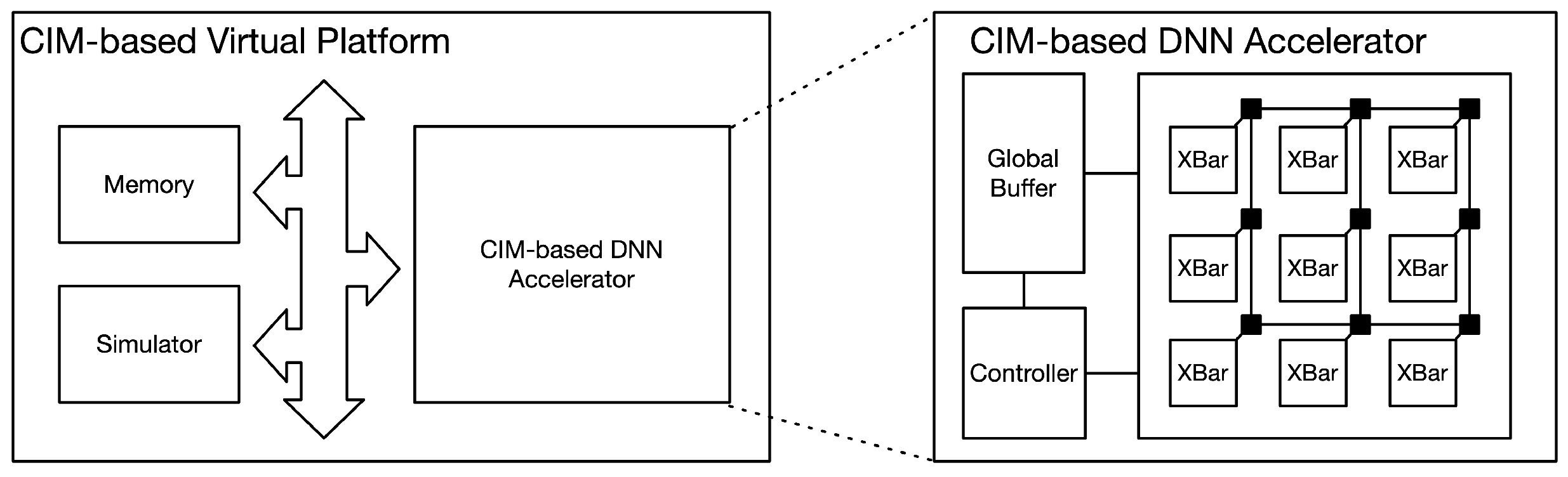
4.5. CIM-Based Virtual Platform
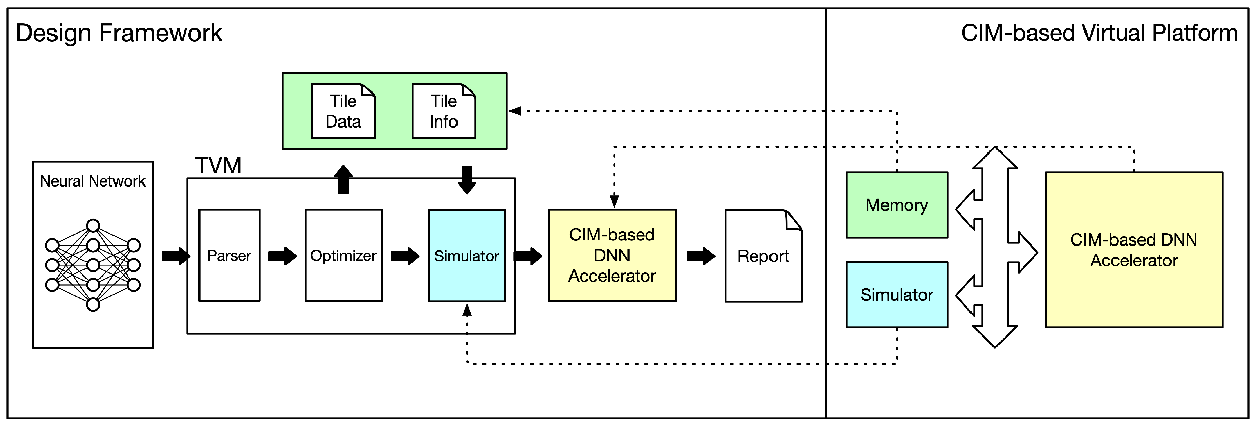
In Figure 8, our demonstrated CIM-based virtual platform, which includes a simulator (in CPU), DRAM and CIM-based DNN accelerator based on SystemC. In brevity, the simulator controls whole data scheduling. More detailed information of simulator and the whole design framework will be discussed in Section 5. Data will be partitioned into several computing tiles due to resource limitation, such as global buffer storage size on DNN accelerator. Each tile of data will be transferred to an accelerator one after another until whole computation is completed. As a result, we can obtain both model accuracy and practical hardware performance from virtual platform.
In addition, if necessary, we can also extend this platform to cycle accuracy for both computation and communication. This extension can make the simulation result closer to the real hardware circuit behavior, but requires a longer simulation time. Because SystemC is a flexible programming language based on C++, we can inherit original hardware class and overwrite original function to rebuild cycle accurate function in the computation module and communication bus. In the cycle accurate function, the hardware behavior is defined with each cycle. Moreover, we can also add latency and power consumption of each action in the program to model real hardware overhead. Additionally, in the communication bus, TLM only concerns the time data starting to transfer and to receive. We can add more detailed behavior such as handshake protocol of bus in each cycle to achieve cycle accurate modeling.

5. Design Framework

The overview of the proposed design framework is displayed in Figure 9. Since the CIM-based virtual platform is embedded into the design flow, for explanation, we use colors and dotted lines to connect both the virtual platform and the whole design framework. The proposed design framework includes a compiler TVM, which is a modern open-source compiler for DNN accelerator, and a CIM-based virtual platform. Our framework takes a model as the input and outputs a report that includes accuracy, hardware cost, and performance evaluation.
Initially, our virtual platform builds the CIM-based DNN accelerator based on hardware configuration. The hardware configuration, such as XBar array height/width, on-chip memory size, etc., are defined by designers. Note that we modularize each component in our accelerator and establish the whole system by TLM-based bus. Thus, the throughput is not only limited by basic components like XBar array size or on-chip storage, but also the bus bandwidth. In this way, we can accurately estimate the performance (closer to the performance of the real system).
After that, our framework starts to take the DNN model as the input. The compiler parses the DNN model and performs optimization according to hardware information from CIM-based virtual platform. Since the on-chip resources such as storage are limited, we need to analyze model and data dimensions to tile data with the best tile way, which is stored in tile info as shown in Figure 9. This result is generated by the optimizer and is stored in memory like green square shown in Figure 9. We can also treat these as the data stored in the memory in the virtual platform.
When the optimizer finishes the optimization process, the simulator is used to simulate and run DNN model on CIM-based DNN accelerator. In Figure 9, the simulator is in the blue square. Note that the simulator is also a part of CIM-based virtual platform. The simulator utilizes the tile info stored in memory and moves tile data to DNN accelerator cycle by cycle. As shown in Figure 10, our simulator has two steps: mapping and evaluation. The mapping step is to use a memory dataflow to map data from on-chip storage to XBar array. Note that, since the XBar array size is fixed, the data dimension R × S × C , which is mapped to each column, may not be fulfilled in one cycle. Thus, this may downgrade the utilization of XBar array. This situation may also happens to the width of XBar array, which maps data dimension M to represent different output channels.
The evaluation step in our simulator has two parts: the inference accuracy and the hardware costs. The inference accuracy evaluation is based on the non-linear functions we embed in ReRAM behavior model. In XBar level, we consider both sneak path and leakage current according to cell’s location in the array. In cell level, we consider lognormal distribution. Quantization errors are applied to both DAC and ADC. Thus, the virtual platform can represent the inference accuracy with non-linear effects considered. On the other hand, we use systemc and TLM modeling method to model the whole behavior of CIM-based DNN accelerator. The evaluator can obtain cycle time, area, power consumption, latency, and the utilization in each layer with respect to the given technology library.

6. Experiment Results

In this section, we demonstrate the experiment results. Note that our ReRAM model is based on the equations in [33]. Table 2 tabulates the values of parameters (for ReRAM model) used in the experiments. In Table 2, I 0 , g 0 and V 0 represent ReRAM fitting parameters, G m a x / G m i n represent ReRAM Max/Min conductance, and T 0 represents ambient temperature of device (for taking thermostatic behavior into account). In Section 6.1, we use Hspice simulation to validate the ReRAM behavior of our design framework. In Section 6.2, we report the inference accuracies of DNN models. In Section 6.3, we report the inference accuracy with respect to different On/Off ratios. In Section 6.4, we report the utilization in each layer with respect to different array sizes. In Section 6.5, we observe the trade-offs between power dissipation and circuit area with respect to different hardware configurations.

6.1. Validation of ReRAM Model

First, we use Spice model to validate the consistency of ReRAM behavior with our program. Based on the values of parameters listed in Table 2, we use the Spice model in [33] and simulate with Hspice tool. In the experiment, we build a ReRAM array and randomly generate different input patterns to observe the accumulate current. In Figure 11, we display the results of the ideal case, the spice model and our program with respect to 8 × 8 , 16 × 16 , 32 × 32 array sizes. In the ideal case, we assume a ReRAM cell in HRS state has no current throw through it. In our program, we calculate the leakage current with the noise model. As shown in Figure 11, we find our program has a very similar trend versus the spice model. It proves that our program can get a practical result. Note that the deviation between the ideal case and the spice model is small because the on/off ratio of ReRAM is big. Thus, in overall, the effect of leakage current is not obvious.

6.2. Accuracy Evaluation

In the experiments, we use four DNN models, including LeNet, AlexNet, VGG-8 and VGG-16, to evaluate the proposed design framework. Note that the number of convolution layers increases as the progress of DNN models. For example, the difference between VGG-8 and VGG-16 is the number of convolution layers. The detailed information of these DNN models is tabulated in Table 3. Although the number of convolution layers in AlexNet is the same as that in VGG-8, on average, the number of channels of each layer in VGG-8 is deeper than that in AlexNet. More convolutions and deeper layers cause error accumulation fast. This also highlights the demand of a design framework that can simulate a DNN accelerator with ReRAM noise considered.
We use these DNN models to evaluate the proposed design framework. We compare their inference accuracies with respect to 32 × 32 , 64 × 64 , 128 × 128 and 256 × 256 array sizes, respectively. Figure 12 provides the top-5 accuracy of each DNN model with respect to different array sizes. As shown in Figure 12, VGG-16 and VGG-8 achieve higher accuracy, while AlexNet and LeNet have lower accuracy. As the array size grows, the accuracy of each model downgrades because of the accumulation of errors. The accuracy from array size 32 × 32 to array size 256 × 256 at least loses 10% accuracy. It means that the array size of CIM-based DNN accelerator needs to be limited. Another observation shows that the downgrade speed is faster for modern DNN models with deeper structures. In Figure 12, VGG-16 has higher accuracy than VGG-8 when array size is 32 × 32 , but VGG-8 has higher accuracy than VGG-16 when array size is 256 × 256 (since the accumulation of errors limit the accuracy of VGG-16 model). Thus, we need to be more careful on modern DNN models.

6.3. On/Off Ratio of ReRAM

In Figure 13, we use LeNet with MNSIT dataset as an example to report the inference accuracy with respect to different combinations of On/Off ratio and array size. Note that On/Off ratio is determined as the resistance ratio of HRS/LRS of ReRAM. High On/Off ratio causes large power consumption but little misunderstanding overlap state. Additionally, high On/Off ratio needs more long latency to write resistance. In contrast, small On/Off ratio has little power consumption and short write resistance state. Thus, this is a trade-off between latency, power consumption and accuracy.
In Figure 13, we consider four kinds of On/Off ratio, including 300, 100, 25 and 10, respectively. Additionally, we consider 32 × 32 , 64 × 64 , 128 × 128 and 256 × 256 array sizes, respectively. We observe that high On/Off ratio can holdout error accumulation. As shown in Figure 13, the accuracy is almost the same when On/Off ratio is between 300 and 100. It means that On/Off ratio 100 is enough to distinguish the states. The accuracy starts to downgrade when On/Off ratio is 25. The accuracy drops worse when On/Off ratio decreases to 10. We can find that the average accuracy loses about 20% in the average line chart. Besides, we also find that a small array size accumulates little error. Thus, a small array size has a small impact on the accuracy loss. We can conclude that: if we want to use large array size, high On/Off ratio is necessary. If we have small XBar array size, we can try to use little XBar array to improve latency and power consumption. Large array size can improve throughput, but needs large On/Off ratio which introduces high latency and high power consumption. Small array size can use small On/Off ratio, but needs to compute more clock cycles. The designer cannot know which is the best architecture of DNN accelerator. It proves that a design framework is necessary to simulate and explore the best result.

6.4. Utilization Evaluation

We use VGG-16 to study the utilization in different layers with respect to different array sizes. Note that VGG-16 has thirteen convolution layers and three fully connected layers. Because the bottleneck of performance occurs in convolution layers, here we focus on the utilization in convolution layers. In Figure 14, we evaluate the VGG16 model with an array size from 16 × 16 to 1024 × 1024 . Note that we assume there is only one XBar in the CIM-based DNN accelerator.
From Figure 14, we have two observations. First, each layer cannot be computed on full XBar with 100% utilization due to CIM dataflow with architecture properties. For example, a layer with kernel size 3 × 3 only can put a channel on a column each cycle. Thus, the utilization can just achieve 9 16 = 56.3 % in array size 16 × 16 . Note that the utilization is the same in each layer for array size 16x16 because it is small enough and hence the data in each layer can be put on XBar equally. The second observation is the utilization of CIM-based DNN accelerator is not proportional to array size. The utilization depends on data dimension of layer and array size. In general, utilization will be promoted when array size gets larger. However, there are some cases where the array size is too large (i.e., larger than processing data). For instance, conv1_1’s input channel is 3; thus, the utilization downgrades when array size is larger than 64. The same situation may happen in each layer and also may happen in different array sizes. It means that we need to give up the concept that a larger array size is better when designing XBar array size. In this dataflow, k 2 × c must be divisible by the number of columns in XBar, where k is kernel size and c is the number of input channels. Output channels of the layer must be divisible by the number of rows in XBar. In this way, the model can be computed efficiently.

6.5. Energy Delay Area Product

We use VGG-8 as an example to evaluate EDAP (energy delay area product) with respect to different array sizes. EDAP is the product of energy, delay and area. This is an indicator of hardware performance and cost. In Figure 15, we demonstrate the result of EDAP from XBar array size 8 × 8 to XBar array size 128 × 128 . In this experiment, we assume there is one XBar array in our CIM-based DNN accelerator. In addition, we normalize the results because the numbers after EDAP are difficult to read. Note that the lower number of energy, delay and area are better. Thus, we want to find an XBar array size with low EDAP.
In Figure 15, the lowest EDAP in the chart is 32 × 32 . We can observe that there is a smile curve. The highest and second high EDAP happen on array size 128 × 128 and array size 8 × 8 , respectively, which are the largest array size and the smallest array size. In array size 8 × 8 , although its latency and area are small, it needs more clock cycles to complete the whole computations, which cause large energy consumption. In contrast, although array size 128 × 128 can have large throughput, dataflow and CIM array properties limit the utilization (as discussed in Section 6.4). Thus, the benefit brought by large array size cannot offset other costs. This result also proves that large or small scale of array size are not the best choice. Designers need a design framework to help to determine the best hardware architecture for DNN model.

7. Conclusions

In this paper, we propose a design framework with SystemC virtual platform to support ReRAM-based deep learning accelerators. In the experiments, we have validated our design framework with Spice model. We also have used our design framework to observe accuracy, On/Off ratio, utilization and EDAP. For example, we find that the accuracy from array size 32 × 32 to array size 256 × 256 at least loses 10% accuracy. The experiment proves that our design framework can help designers to determine hardware architecture with accuracy and hardware costs considered.

Author Contributions

Conceptualization, methodology, and formal analysis, H.-Y.K., S.-H.H. and W.-K.C.; investigation and writing—original draft preparation, H.-Y.K.; supervision and writing—review and editing, S.-H.H. and W.-K.C. All authors have read and agreed to the published version of the manuscript.

Funding

This work was supported in part by the Ministry of Science and Technology, Taiwan, under grant number MOST 110-2218-E-033-003.

Institutional Review Board Statement

Not applicable.

Informed Consent Statement

Not applicable.

Data Availability Statement

The data used to support the findings of this study are included in this paper.

Conflicts of Interest

The authors declare no conflict of interest.

References

  1. Krizhevsky, A.; Sutskever, I.; Hinton, G.E. ImageNet classification with deep convolutional neural networks. Commun. ACM 2017, 60, 84–90. [Google Scholar] [CrossRef]
  2. Simonyan, K.; Zisserman, A. Very Deep Convolutional Networks for Large-Scale Image Recognition. arXiv 2014, arXiv:1409.1556. [Google Scholar]
  3. He, K.; Zhang, X.; Ren, S.; Sun, J. Deep Residual Learning for Image Recognition. In Proceedings of the 2016 IEEE Conference on Computer Vision and Pattern Recognition (CVPR), Las Vegas, NV, USA, 27–30 June 2016; pp. 770–778. [Google Scholar] [CrossRef] [Green Version]
  4. Iandola, F.N.; Han, S.; Moskewicz, M.W.; Ashraf, K.; Dally, W.J.; Keutzer, K. SqueezeNet: AlexNet-level accuracy with 50× fewer parameters and <0.5 MB model size. arXiv 2016, arXiv:1602.07360. [Google Scholar]
  5. Huang, G.; Liu, Z.; Maaten, L.V.D.; Weinberger, K.Q. Densely Connected Convolutional Networks. In Proceedings of the 2017 IEEE Conference on Computer Vision and Pattern Recognition (CVPR), Honolulu, HI, USA, 21–26 July 2017; pp. 2261–2269. [Google Scholar] [CrossRef] [Green Version]
  6. Lu, W.; Yan, G.; Li, J.; Gong, S.; Han, Y.; Li, X. FlexFlow: A Flexible Dataflow Accelerator Architecture for Convolutional Neural Networks. In Proceedings of the 2017 IEEE International Symposium on High Performance Computer Architecture (HPCA), Austin, TX, USA, 4–8 February 2017; pp. 553–564. [Google Scholar] [CrossRef]
  7. Wang, Y.; Wang, Y.; Li, H.; Shi, C.; Li, X. Systolic Cube: A Spatial 3D CNN Accelerator Architecture for Low Power Video Analysis. In Proceedings of the 56th Annual Design Automation Conference 2019, Las Vegas, NV, USA, 2–6 June 2019; pp. 1–6. [Google Scholar] [CrossRef]
  8. Du, Z.; Fasthuber, R.; Chen, T.; Ienne, P.; Li, L.; Luo, T.; Feng, X.; Chen, Y.; Temam, O. Shidiannao: Shifting Vision Processing Closer to the Sensor. In Proceedings of the 2015 ACM/IEEE 42nd Annual International Symposium on Computer Architecture (ISCA), Portland, OR, USA, 13–17 June 2015; Volume 43, pp. 92–104. [Google Scholar] [CrossRef]
  9. Kwon, H.; Samajdar, A.; Krishna, T. MAERI: Enabling Flexible Dataflow Mapping over DNN Accelerators via Reconfigurable Interconnects. ACM SIGPLAN Not. 2018, 53, 461–475. [Google Scholar] [CrossRef]
  10. Chen, Y.H.; Emer, J.; Sze, V. Eyeriss: A Spatial Architecture for Energy-Efficient Dataflow for Convolutional Neural Networks. In Proceedings of the 2016 ACM/IEEE 43rd Annual International Symposium on Computer Architecture (ISCA), Seoul, Korea, 18–22 June 2016; Volume 44, pp. 367–379. [Google Scholar] [CrossRef] [Green Version]
  11. Chen, Y.H.; Krishna, T.; Emer, J.S.; Sze, V. Eyeriss: An Energy-Efficient Reconfigurable Accelerator for Deep Convolutional Neural Networks. IEEE J. Solid-State Circuits 2017, 52, 127–138. [Google Scholar] [CrossRef] [Green Version]
  12. Chen, Y.H.; Yang, T.J.; Emer, J.; Sze, V. Eyeriss v2: A Flexible Accelerator for Emerging Deep Neural Networks on Mobile Devices. IEEE J. Emerg. Sel. Top. Circuits Syst. 2019, 9, 292–308. [Google Scholar] [CrossRef] [Green Version]
  13. Zhao, Y.; Chen, X.; Wang, Y.; Li, C.; You, H.; Fu, Y.; Xie, Y.; Wang, Z.; Lin, Y. SmartExchange: Trading Higher-cost Memory Storage/Access for Lower-cost Computation. In Proceedings of the 2020 ACM/IEEE 47th Annual International Symposium on Computer Architecture (ISCA), Valencia, Spain, 30 May–3 June 2020; pp. 954–967. [Google Scholar] [CrossRef]
  14. Chatarasi, P.; Kwon, H.; Raina, N.; Malik, S.; Haridas, V.; Parashar, A.; Pellauer, M.; Krishna, T.; Sarkar, V. Marvel: A Data-centric Compiler for DNN Operators on Spatial Accelerators. arXiv 2020, arXiv:2002.07752. [Google Scholar]
  15. Kwon, H.; Chatarasi, P.; Pellauer, M.; Parashar, A.; Sarkar, V.; Krishna, T. Understanding Reuse, Performance, and Hardware Cost of DNN Dataflows: A Data-Centric Approach Using MAESTRO. arXiv 2020, arXiv:1805.02566. [Google Scholar]
  16. Shafiee, A.; Nag, A.; Muralimanohar, N.; Balasubramonian, R.; Strachan, J.P.; Hu, M.; Williams, R.S.; Srikumar, V. ISAAC: A Convolutional Neural Network Accelerator with In-Situ Analog Arithmetic in Crossbars. In Proceedings of the 2016 ACM/IEEE 43rd Annual International Symposium on Computer Architecture (ISCA), Seoul, Korea, 18–22 June 2016; Volume 44, pp. 14–26. [Google Scholar] [CrossRef]
  17. Chi, P.; Li, S.; Xu, C.; Zhang, T.; Zhao, J.; Liu, Y.; Wang, Y.; Xie, Y. PRIME: A Novel Processing-in-Memory Architecture for Neural Network Computation in ReRAM-Based Main Memory. In Proceedings of the 2016 ACM/IEEE 43rd Annual International Symposium on Computer Architecture (ISCA), Seoul, Korea, 18–22 June 2016; Volume 44, pp. 27–39. [Google Scholar] [CrossRef]
  18. Wong, H.S.P.; Lee, H.Y.; Yu, S.; Chen, Y.S.; Wu, Y.; Chen, P.S.; Lee, B.; Chen, F.T.; Tsai, M.J. Metal–Oxide RRAM. Proc. IEEE 2012, 100, 1951–1970. [Google Scholar] [CrossRef]
  19. Park, J. Neuromorphic Computing Using Emerging Synaptic Devices: A Retrospective Summary and an Outlook. Electronics 2020, 9, 1414. [Google Scholar] [CrossRef]
  20. Mittal, S. A Survey of ReRAM-Based Architectures for Processing-In-Memory and Neural Networks. Mach. Learn. Knowl. Extr. 2018, 1, 5. [Google Scholar] [CrossRef] [Green Version]
  21. Feinberg, B.; Wang, S.; Ipek, E. Making Memristive Neural Network Accelerators Reliable. In Proceedings of the 2018 IEEE International Symposium on High Performance Computer Architecture (HPCA), Vienna, Austria, 24–28 February 2018; pp. 52–65. [Google Scholar] [CrossRef]
  22. Wang, S.; Jin, S.; Bai, D.; Fan, Y.; Shi, H.; Fernandez, C. A critical review of improved deep learning methods for the remaining useful life prediction of lithium-ion batteries. Energy Rep. 2021, 7, 5562–5574. [Google Scholar] [CrossRef]
  23. Wang, S.; Takyi-Aninakwa, P.; Jin, S.; Yu, C.; Fernandez, C.; Stroe, D.I. An improved feedforward-long short-term memory modeling method for the whole-life-cycle state of charge prediction of lithium-ion batteries considering current-voltage-temperature variation. Energy 2022, 254, 124224. [Google Scholar] [CrossRef]
  24. Xia, L.; Li, B.; Tang, T.; Gu, P.; Chen, P.Y.; Yu, S.; Cao, Y.; Wang, Y.; Xie, Y.; Yang, H. MNSIM: Simulation Platform for Memristor-Based Neuromorphic Computing System. IEEE Trans. Comput.-Aided Des. Integr. Circuits Syst. 2018, 37, 1009–1022. [Google Scholar] [CrossRef]
  25. Rasch, M.J.; Moreda, D.; Gokmen, T.; Gallo, M.L.; Carta, F.; Goldberg, C.; Maghraoui, K.E.; Sebastian, A.; Narayanan, V. A flexible and fast PyTorch toolkit for simulating training and inference on analog crossbar arrays. arXiv 2021, arXiv:2104.02184. [Google Scholar]
  26. Bahar, I.; Lin, M.Y.; Cheng, H.Y.; Lin, W.T.; Yang, T.H.; Tseng, I.C.; Yang, C.L.; Hu, H.W.; Chang, H.S.; Li, H.P.; et al. DL-RSIM: A simulation framework to enable reliable ReRAM-based accelerators for deep learning. In Proceedings of the 2018 IEEE/ACM International Conference on Computer-Aided Design (ICCAD), San Diego, CA, USA, 5–8 November 2018; pp. 1–8. [Google Scholar] [CrossRef]
  27. Chen, P.Y.; Peng, X.; Yu, S. NeuroSim+: An Integrated Device-to-Algorithm Framework for Benchmarking Synaptic Devices and Array Architectures. In Proceedings of the 2017 IEEE International Electron Devices Meeting (IEDM), San Francisco, CA, USA, 2–6 December 2017; pp. 6.1.1–6.1.4. [Google Scholar] [CrossRef]
  28. Mohsenin, T.; Zhao, W.; Chen, Y.; Mutlu, O.; Zhu, Z.; Sun, H.; Qiu, K.; Xia, L.; Krishnan, G.; Dai, G.; et al. MNSIM 2.0: A Behavior-Level Modeling Tool for Memristor-based Neuromorphic Computing Systems. In Proceedings of the 2020 on Great Lakes Symposium on VLSI, Online, 7–9 September 2020; pp. 83–88. [Google Scholar] [CrossRef]
  29. Chen, P.Y.; Peng, X.; Yu, S. NeuroSim: A Circuit-Level Macro Model for Benchmarking Neuro-Inspired Architectures in Online Learning. IEEE Trans. Comput.-Aided Des. Integr. Circuits Syst. 2018, 37, 3067–3080. [Google Scholar] [CrossRef]
  30. Xia, L.; Li, B.; Tang, T.; Gu, P.; Yin, X.; Huangfu, W.; Chen, P.Y.; Yu, S.; Cao, Y.; Wang, Y.; et al. System Simulation of Memristor Based Computation In Memory Platforms. In Proceedings of the 2016 Design, Automation & Test in Europe Conference & Exhibition (DATE), Dresden, Germany, 14–18 March 2016; pp. 469–474. [Google Scholar] [CrossRef]
  31. BanaGozar, A.; Vadivel, K.; Stuijk, S.; Corporaal, H.; Wong, S.; Lebdeh, M.A.; Yu, J.; Hamdioui, S. CIM-SIM: Computation In Memory SIMuIator. In Proceedings of the 22nd International Workshop on Software and Compilers for Embedded Systems, Sankt Goar, Germany, 27–28 May 2019; pp. 1–4. [Google Scholar] [CrossRef] [Green Version]
  32. Galicia, M.; Merchant, F.; Leupers, R. A Parallel SystemC Virtual Platform for Neuromorphic Architectures. arXiv 2021, arXiv:2112.13157. [Google Scholar]
  33. Guan, X.; Yu, S.; Wong, H.S.P. A SPICE Compact Model of Metal Oxide Resistive Switching Memory with Variations. IEEE Electron Device Lett. 2012, 33, 1405–1407. [Google Scholar] [CrossRef]
Figure 1. Concept of convolution neural network.
Electronics 11 02107 g001
Figure 2. (a) A ReRAM column. (b) ReRAM array.
Electronics 11 02107 g002
Figure 3. Dataflow of CIM.
Electronics 11 02107 g003
Figure 4. Noise overview in ReRAM array.
Electronics 11 02107 g004
Figure 5. (a) Conducting Filament of ReRAM. (b) Lognormal distribution of ReRAM.
Electronics 11 02107 g005
Figure 6. (a) Leakage current. (b) Sneak path.
Electronics 11 02107 g006
Figure 7. XBar architecture and ReRAM array model.
Electronics 11 02107 g007
Figure 8. Virtual platform and CIM-based DNN accelerator.
Electronics 11 02107 g008
Figure 9. XBar architecture and ReRAM array model.
Electronics 11 02107 g009
Figure 10. XBar architecture and ReRAM array model.
Electronics 11 02107 g010
Figure 11. Accumulated result of ReRAM array.
Electronics 11 02107 g011
Figure 12. Accuracy of DNN models with different array sizes.
Electronics 11 02107 g012
Figure 13. Accuracy with respect to different On/Off ratios and different array sizes.
Electronics 11 02107 g013
Figure 14. Utilization with respect to different array sizes and layers on VGG-16.
Electronics 11 02107 g014
Figure 15. EDAP of different array sizes.
Electronics 11 02107 g015
Table 1. Comparisons of the proposed design framework with previous works.
FrameworkSystem LevelVirtual PlatformLognormal DistributionNon-Linear Properties Leakage CurrentSneak PathIR DropHW Cost
[24]
[25]
[26]
[27]
[28]
[29]
[30]
[31]
[32]
Ours
Table 2. Fitting parameters.
ParametersValueDescription
I 0 6.14 × 10 5 I-V fitting parameter
g 0 2.75 × 10 10 I-V fitting parameter
V 0 0.43 I-V fitting parameter
T 0 293 KAmbient temperature
G m a x / G m i n 100/0.33 μ SReRAM Max/Min conductance
Table 3. Information of DNN models.
ModelsInput ShapeNumber of Convolution Layers
LeNet 32 × 32 3
AlexNet 224 × 224 5
VGG-8 224 × 224 5
VGG-16 224 × 224 13
Publisher’s Note: MDPI stays neutral with regard to jurisdictional claims in published maps and institutional affiliations.

