1. Introduction
Throughout the last decades, academic and industrial concern has been increasingly dedicated to the development of fully integrable electronic solutions for a variety of low-size, low-cost, and low-power applications. Significant examples regard wearable and implantable sensing devices [
1,
2], wireless sensor networks [
3,
4], and biomedical systems [
5]. As a consequence of the challenging requirements demanded by such an innovative application framework, the design of reliable fully integrated frequency references has emerged as a very relevant research trend.
The most common solution to provide a reference frequency to digital circuits and communication systems is using an oscillator that relies on an off-chip resonator [
6]. However, oscillators based on crystal resonators are sub-optimal for the above-mentioned applications, due to their relatively high cost and the necessity of a bulky off-chip component. As for LC-tank or transmission line resonators, fully integrated versions are very demanding in terms of silicon area and are limited to frequencies in the GHz range, involving high power consumption. Therefore, thanks to their small area requirements, inductor-less fully integrable oscillators, such as relaxation oscillators, are to be preferred in applications where it is crucial to minimize size, cost, and power consumption.
In a comparator-based relaxation oscillator, the oscillation is due to a capacitor being periodically charged and discharged by means of resistors (
RC oscillators) [
7] or constant current generators (I-C oscillators) [
8]. However, the appealing properties of relaxation oscillators are typically traded off with lacking performances for their reliability: the frequency accuracy and stability are usually far from optimal, due to process–voltage–temperature (PVT) variations. For practical relaxation oscillator uses, the frequency inaccuracies can be partially relieved by means of a proper trimming, which might be executed as part of the fabrication process (as is performed for the internal oscillators of many low-cost microcontroller families, to compensate for process variations [
9,
10]) or even at operating time [
11]. Moreover, regarding the supply voltage sensitivity, an on-chip regulator is most likely present in a system-on-chip (SoC), to provide a stable supply voltage to the oscillator and other sub-circuits. As an alternative to such standard approaches, design strategies specifically aimed at reducing the PVT sensitivity of the oscillation frequency have been proposed. To this purpose, a possible approach, proposed in [
12], is to employ an I-C relaxation oscillator equipped with a process-compensated current reference. Promising results have been reported for the process sensitivity of the generated frequency; however, the choice of an I-C operating principle generally worsens the phase noise and jitter performances, due to the relevant noise contribution (both thermal and flicker) from the current reference itself.
Another crucial aspect in the design of a relaxation oscillator regards the phase noise reduction. Standard relaxation oscillators are characterized by poor phase noise and jitter performances, giving rise to significant timing uncertainties in the generated waveform. The jitter accumulation phenomenon, in particular, can be especially harmful in many applications. Regarding the generation of reference clocks for asynchronous serial communication protocols, the jitter accumulated in the medium/long term might force one to frequently resynchronize the clocks of the communicating devices. Furthermore, the jitter accumulation can give rise to relevant sampling errors in analog-to-digital converters (ADCs), in addition to the quantization noise [
13], and more in general, can contribute to the output noise in switched-capacitor (SC) circuits [
14]. Many valid approaches have been proposed to deal with the above-mentioned problems; nevertheless, optimal design strategies able to concurrently provide valuable results for both the PVT sensitivity and the phase noise are yet to be demonstrated.
In this work, we mainly focused on improving the phase noise performances. Various ad hoc compensation techniques have been proposed in this respect. Generally, if a low-phase-noise relaxation oscillator is desired, an
RC operating principle is to be preferred. That is because the resistor noise, taking the place of the noise brought by the reference current, presents a negligible flicker component and, hence, allows for a better phase noise performance [
15]. However, such a design choice alone is insufficient to achieve competitive phase noise performances.
Swing-boosting (SB) techniques are very common [
16,
17,
18], aiming at widening the swing of the capacitor voltage by means of SC circuits. Specifically, the latter are used to boost the capacitor voltage at the beginning of every half-period. As we recall in
Section 2, this directly results in a decrease of the jitter variance. However, if the capacitor voltage is boosted even above the supply voltage and below ground, the compatibility with standard n-well CMOS processes might be lost. That is because it is unfeasible to prevent the drain-body junctions of n pass transistors from conducting, whereas the drain voltage becomes lower than the ground voltage.
Solutions employing a voltage averaging feedback (VAF) have also been proposed [
19,
20], based on a continuous-time integrating feedback loop acting on the comparator thresholds. Nonetheless, while the comparator noise is effectively reduced, additional unprocessed noise is introduced by the amplifier in the feedback path. The
RC oscillator presented in [
21] is provided with a similar integrated error feedback (IEF) technique, alongside with a chopping approach against noise sources in the feedback path, but a sub-optimal phase noise is ultimately obtained far from the carrier frequency and the circuit complexity is considerable. A voltage feedback (yet operating in the discrete time) is present also in the latch-based oscillator reported in [
16], combined with the SB approach, but its purpose is mainly to reduce the mismatch-related frequency inaccuracy rather than the jitter. In [
22], a technique based on the injection of an anti-jitter charge package into the timing capacitor is proposed, but a dual-comparator architecture is required. Besides, the duty cycle of the output waveform is prevented from being equal to 50%, unless additional circuitry is employed. In [
23], an effective compensation technique based on periodic autozero phases was presented, but it can be applied only to dual-comparator
RC oscillators, with both the comparators always powered-on.
In this paper, we propose a novel comparator self-threshold-adjustment (CSTA) technique. It is able to process the comparator threshold noise by means of a modified version of correlated double sampling (CDS), which, differently from standard CDS, is free from contribution of noise fold-over at low frequencies. This is attained by quite a simple architecture, automatically performing a proper sampling of the threshold errors, and employing such error samples in a discrete-time feedback loop. The noise sampling takes place concurrently with the normal operation of the oscillator core, without the need of additional autozero phases.
This paper is organized as follows. In
Section 2, the origin of the jitter in
RC oscillators is reviewed, introducing possible solutions for its reduction. Afterwards, in
Section 3, we introduce the CSTA technique, critically discussing its effect on the phase noise. Details regarding the transistor-level implementation of a CSTA-compensated
RC relaxation oscillator are provided in
Section 4, referring to a commercial 0.18 µm CMOS process. The results obtained from accurate electrical simulations of such a circuit design are reported and discussed in
Section 5. Then, the paper is concluded with
Section 6, where we propose our final considerations.
2. Theoretical Insight
A theoretical premise is presented in this section, regarding the most relevant aspects involved in the design of a low-phase-noise relaxation oscillator. In doing so, general design guidelines for the reduction of the jitter (especially the jitter accumulated in the medium/long term) are identified.
To quantify the phase noise, the single-sided power spectral density (PSD) of the output signal, normalized by the power of the fundamental harmonic, is commonly employed [
24]. As it is well known, it typically exhibits a 1/
f3 trend close to the carrier frequency, which is due to flicker noise sources; conversely, the 1/
f2 noise prevailing at higher offset frequencies is related to white noise sources [
25]. As for the jitter, we will mainly refer to the notion of period jitter
pm, defined as the timing uncertainty affecting the duration of the generic
m-th oscillation cycle. The accumulated jitter is simply given by the summation of the period jitter samples throughout a certain number of consecutive cycles. One last preliminary aspect to be considered is that, based on the relationships binding the jitter and the phase noise, the 1/
f3 and 1/
f2 phase noise components correspond to components of the period jitter PSD which approximately have 1/
f and white trends, respectively [
26].
Typically, the phase noise can be reduced by increasing the power consumption. The following figure of merit (
FoM) [
24] is usually employed to express the phase noise/consumption trade-off:
where
PN(Δ
f) is the phase noise, evaluated at a Δ
f offset frequency from the fundamental frequency
f0, and
P is the average power consumption of the oscillator.
For every
RC relaxation oscillator, the period jitter includes at least two independent contributions, as indicated in Equation (2): one is due to the comparator threshold noise and the other arises from the
kT/
C noise, implied by the charging/discharging process of the capacitor itself.
In this relationship, the subscript
m indicates the generic
m-th oscillation cycle. In elementary comparator-based relaxation oscillators, the comparator-related component is typically the main contributor to the phase noise. This is highly unideal, since the comparator noise usually includes significant 1/
f flicker noise [
27], which translates into 1/
f3 close-in phase noise [
28]. The 1/
f3 phase noise, dominant at low offset frequencies, causes the long-term accumulated jitter to be especially high, due to its autocorrelation properties. Hence, to the purpose of mitigating the jitter accumulation, oscillator topologies that intrinsically apply flicker-noise-reduction mechanisms should be used.
In relaxation oscillators, the period jitter is given by a topology-dependent combination of voltage noise samples taken at the comparator switching instants. That is because, in every half-period of the oscillation, the capacitor voltage reaches the comparator threshold with a stochastic timing error, dependent on the noise sources. We will show that, employing proper relaxation oscillator topologies, the above-mentioned combination of noise samples can result in the standard CDS expression, or other similar discrete-time functions. For the sake of clarity, in Equation (3) we recall the time-domain definition of the effective residual noise
vn-eff at the
m-th clock cycle in the standard CDS:
In this relationship,
vn(
t) is a generic noise process (which may be the comparator noise, in the case of a relaxation oscillator), while
T0 is the sampling period (corresponding to the period of the oscillator output signal). As is well-known, CDS appreciably relieves the effects of flicker noise components. This is achieved at the cost of an increased thermal noise contribution (translating into 1/
f2 phase noise), due to the noise fold-over phenomenon. In
Section 3, completing the analytical treatment hereby proposed, we introduce an original approach for the reduction of the close-in phase noise of
RC oscillators, based on a CDS variant free from low-frequency noise fold-over. For such a reason, rather than being dominated by the comparator threshold noise, the phase noise comes to be mainly due to the
kT/
C noise, even at frequencies close to the carrier.
To the purpose of comparing different
RC oscillators featuring CDS-like comparator-noise-processing mechanisms, we will employ the following formalism. The flicker corner frequency of the comparator noise is assumed to be sufficiently lower than the oscillation frequency, to ensure an effective rejection of the flicker noise itself by means of the CDS-like processing. Under such a hypothesis, the PSD of the discrete-time effective noise resulting from a generic CDS variant can be expressed as in Equation (4).
In this relationship,
NBW is the noise bandwidth of the comparator [
29],
f0 is the oscillation frequency,
is the broad-band (white) component of the comparator noise PSD, and
α is the set of comparator thresholds required by the oscillator, normalized by
Vdd (the number of distinct thresholds depends on the oscillator topology and operating principle).
HS(
α,
f) is a noise-shaping function that depends on the particular CDS variant implemented by the considered oscillator topology and, in some cases, also on the comparator thresholds. In the case of the standard CDS, it is constantly equal to 4.
As we will show later, the two components of the period jitter variance
can be expressed according to Equations (5) and (6) for every
RC oscillator implementing a CDS-like compensation of the comparator noise. As mentioned earlier, the flicker corner frequency is assumed to be lower than the oscillation frequency. Moreover, for a greater simplicity, the presence of the comparator hysteresis and delay is neglected in this simplified model. Equations (5) and (6) can be modified to take into account also non-negligible hysteresis and delay, but this is not necessary for the sake of our considerations.
Comparisons between different RC oscillator topologies concerning their jitter performances can be made by simply referring to the γcomp(α), γkT/C(α) coefficients and the HS(α,f) noise-shaping function. Indeed, such quantities exhaustively account for the relationship between the period jitter variance, the oscillator topology, and the values of the comparator thresholds.
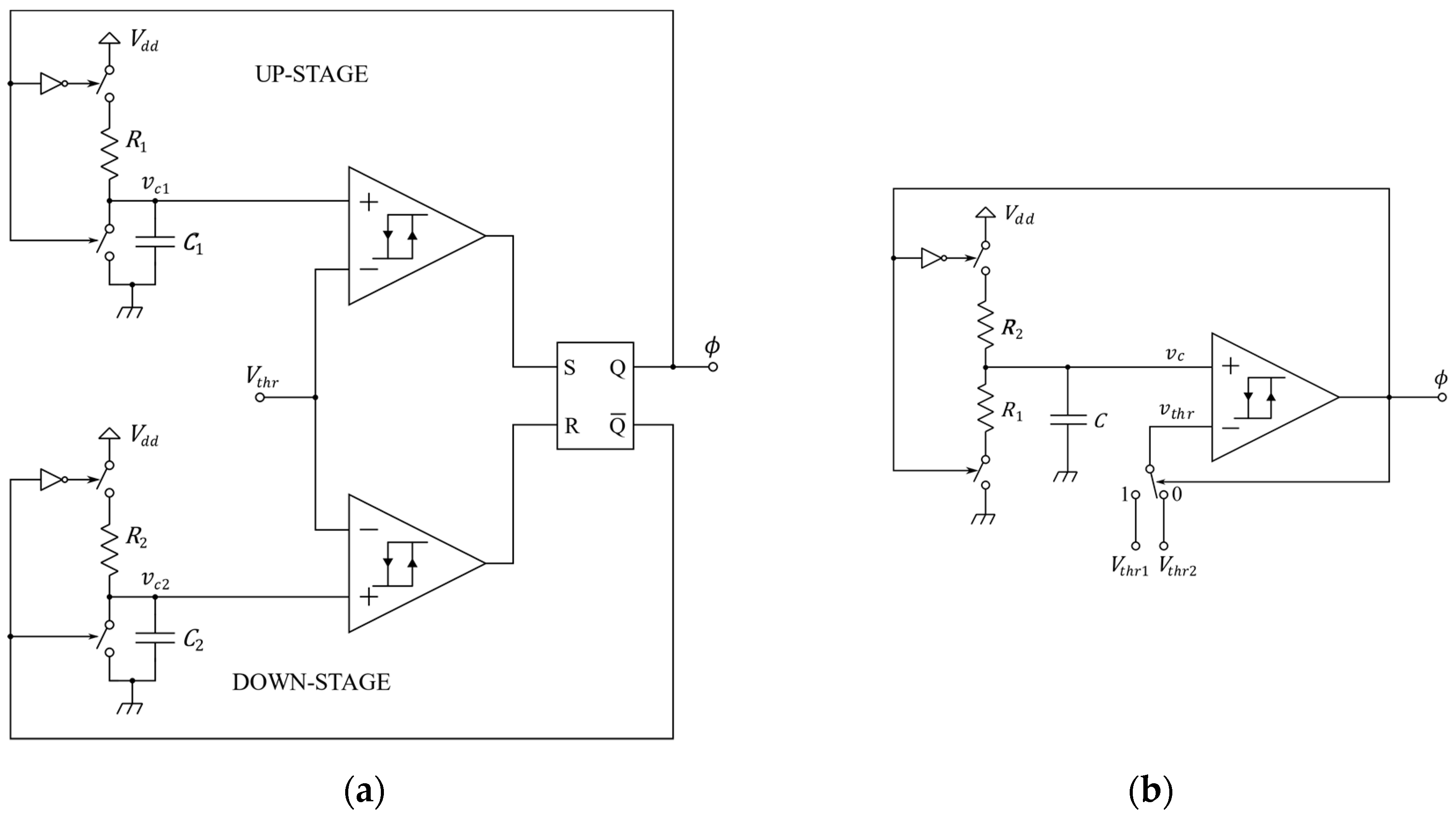
2.1. Elementary RC Relaxation Oscillators
Basic relaxation oscillator topologies cannot be expected to present valuable phase noise performances. Indeed, they process the comparator noise through poorly effective CDS-like techniques or they might not even apply any useful noise-processing whatsoever.
To begin with, we take into consideration the dual-comparator
RC oscillator of
Figure 1a, which is very popular for non-critical applications. The ideal oscillation period of this oscillator is given by the following relationship, valid for
R1 =
R2 =
R,
C1 =
C2 =
C.
where
α Vthr/
Vdd is the comparator threshold normalized by the supply voltage. As for the period jitter, it can be approximately expressed as in Equation (8).
In these equations, the
vn1,2(
t) terms are effective noise processes, related to either the up or down stage of the oscillator. Such effective noise processes are defined based on the following consideration. In an ideally noise-less scenario, each comparator switching event occurs when the related capacitor voltage exactly reaches
Vthr. In the presence of noise, instead, each switching event occurs with a timing uncertainty, due to a stochastic error affecting the comparator threshold. The stochastic threshold errors originate from noise sources within the circuit and can be treated as a referred-to-the-input effective noise process of the comparator. As indicated in Equation (9), the latter include contributions from the comparators threshold noise
vn-comp1,2(
t) itself and the RC-filtered thermal noise of the resistors
vnc1,2(
t). Equation (8) is attained assuming the deterministic component of the capacitor voltage waveform
vc(
t) to be linear around the comparator switching instants. Thereby, the period jitter can be simply expressed as the summation of sampled noise processes divided by the slope of
vc(
t) itself [
30]. For the moment, the comparator hysteresis and delay are neglected in the analysis.
From Equation (8), it is evident how the flicker noise of the comparators does not undergo any beneficial processing: the noise samples of two distinct comparators are simply summed together in Equation (8). Therefore, in this elementary oscillator, the comparator noise should be expected to represent by far the main phase noise contributor, especially at low offset frequencies.
The basic single-comparator
RC oscillator of
Figure 1b offers an improvement for what concerns the discrete-time processing of the comparator noise, since a CDS-like technique is intrinsically applied to the noise of the single comparator. The ideal oscillation period can be easily determined as follows, assuming
R1 =
R2 =
R.
where
α1 and
α2 are the comparator thresholds,
Vthr1 and
Vthr2 (with
Vthr2 >
Vthr1), normalized by
Vdd. The second equality is valid with the choice
α1 +
α2 = 1, ensuring a 50% duty cycle, as required by many applications. To quantify the jitter contribution of the comparator noise, it should be considered that the capacitor voltage does not periodically lose memory of past threshold errors (as it happens, instead, in the dual-comparator
RC oscillator). Consequently, the threshold noise sampled at the end of a half-period also determines an error on the initial capacitor voltage of the subsequent half-period. Through simple calculations, the following relationship can be determined for the comparator-related jitter component, in the case where
α1 +
α2 = 1.
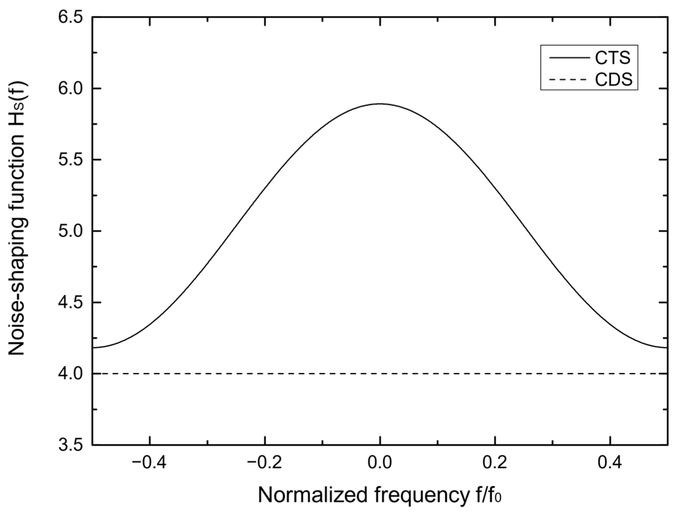
For simplicity purposes, the combination of noise samples enclosed within the square brackets in Equation (11) will be referred to as correlated triple sampling (CTS), since three different samples are combined. Through an analytical treatment analogous to the one commonly presented for the standard CDS [
31], it can be demonstrated that such a discrete-time noise processing is similarly efficient against the flicker noise, at least if the flicker corner frequency is sufficiently lower than the oscillation frequency. However, the fold-over of the thermal noise is worse: while CDS gives rise to a discrete-time effective noise with a white PSD, Equation (11) results in a higher PSD, especially at low frequencies. The
HS(
f) noise-shaping function of CTS is represented in
Figure 2 for
α1,opt ≅ 0.176. This design choice minimizes the comparator noise contribution to the PSD of the period jitter. Such a PSD contribution will be referred to as
in the following.
An optimization of
is possible because, in Equation (11), both the PSD of the effective voltage noise and the time constant
RC depend on
α1, for a given oscillation frequency. Indeed, combining Equations (4), (10) and (11), the following expression is found for the comparator noise contribution to the PSD of the period jitter.
γcomp(
α1) is the same topology-dependent coefficient that was defined according to Equation (5). The way the comparator noise affects the jitter statistics is represented by the product:
which has to be made as small as possible. In the oscillator of
Figure 1b, its optimum DC value is
GDC,min =
G(
α1,opt,0) ≅ 19.95. Topologies that perform better in this respect are illustrated later in this paper.
To summarize, while being, in principle, effective against the flicker noise, CTS still causes relevant close-in phase noise, due to the significant fold-over of the comparator broadband noise at low frequencies. Moreover, if the flicker corner frequency is not low enough (as it is likely to happen in a real design), even the flicker component is folded over, more harmfully than it would be with standard CDS. However, the oscillator of
Figure 1b still represents a significative reference. Because of its simplicity, the calculation of the maximum FoM achievable by
RC oscillators (169 dBc/Hz), first performed in [
15], actually refers to a very similar architecture.
2.2. Maximum Achievable FoM
In this paragraph, we briefly recall the method proposed by Navid et al. [
15] for the determination of the maximum achievable FoM, to provide analytical support to the subsequent considerations. The limit FoM can be determined through a best-case ideal analysis: the comparator is supposed to be completely ideal, only unavoidable white noise sources are assumed to be present, and only the power strictly necessary to periodically charge and discharge the capacitor is taken into account. More specifically, the
kT/
C jitter contribution, arising from sampling the RC-filtered thermal noise of the resistors, is accounted for as the minimum possible jitter: while the comparator-related phase noise might be made negligible by designing a very low-noise comparator or by applying ad hoc noise-reduction techniques, it is obviously unfeasible to analogously reject the resistor thermal noise.
For the simple oscillator of
Figure 1b, the
kT/
C jitter term can be expressed according to the following relationship.
The two noise samples present in Equation (15) are uncorrelated, since they come from the thermal noise of different resistors. Their variance cannot be simply assumed to be equal to
kT/
C: the variance itself of each of the two
vnc1,2(
t) noise processes actually increases from the beginning of the corresponding oscillation half-period, starting from zero and indeed saturating to
kT/
C [
15]. It is initially null because, under the assumption of a completely ideal comparator, at switching instants the capacitor voltage is deterministically equal to one of the comparator thresholds. Based on the equivalent noise circuit of
Figure 3, where the resistor thermal noise is represented by the current generator
in, such a variance can be found to be
If we evaluate Equation (16) at
t ≅
T0/2, divide the result by the slope of the deterministic component of the capacitor voltage, and multiply it by 2 (to account for the jitter affecting both the rising and the falling edges), the variance
of the period jitter can be obtained. At this point, the following relationship between the phase noise and the period jitter can be used [
26]:
This relationship holds true under the simplification of negligible flicker noise sources and, as for the second equality, at frequencies not extremely close to the carrier. Substituting this expression of the phase noise into Equation (1), which indicates the FoM definition, and choosing the comparator thresholds to maximize the FoM itself, the well-known limit value of 169 dBc/Hz is found. To provide an all-round treatment of the jitter-reduction design strategies that we propose, the analysis methodology briefly recalled in this paragraph is applied, in the following, also to the proposed oscillator topologies. It is interesting to notice that, while indeed mitigating the effects of the comparator noise, the proposed design choices imply a slight degradation (however acceptable) of the maximum achievable figure of merit.
2.3. Dual-Slope RC Oscillator with Standard CDS
As shown in the previous paragraph, to apply a CDS-like processing to the comparator threshold noise, the capacitor voltage determining the comparator switching events has to present opposite slopes at the two transitions (high-to-low and low-to-high) of the clock cycle. This ensures that the comparator noise samples contributing to the period jitter are summed together with opposite signs [
30]. An analogous result can be attained also by employing a single-slope sawtooth-like waveform as the comparator input voltage and switching the comparator inputs half-period by half-period, through a switching matrix [
12]. The elementary oscillator of
Figure 1b satisfies the dual slope requirement but still implies quite relevant low-frequency noise fold-over. A better-performing noise-processing mechanism is desirable, to the aim of reducing the close-in phase noise. A simple modification of such an architecture, resulting in a dual-slope
RC oscillator able to process the comparator noise through the standard CDS, implies the use of two distinct capacitors, as shown in
Figure 4.
The two capacitors complementarily undergo two different working phases: a charging phase, by means of the resistors, to provoke the subsequent switching event of the comparator, and a discharging phase, through a switch. To obtain a 50% duty cycle, the following design choices have to be made:
C1 =
C2 =
C,
R1 =
R2 =
R,
Vthr1 +
Vthr2 =
Vdd.
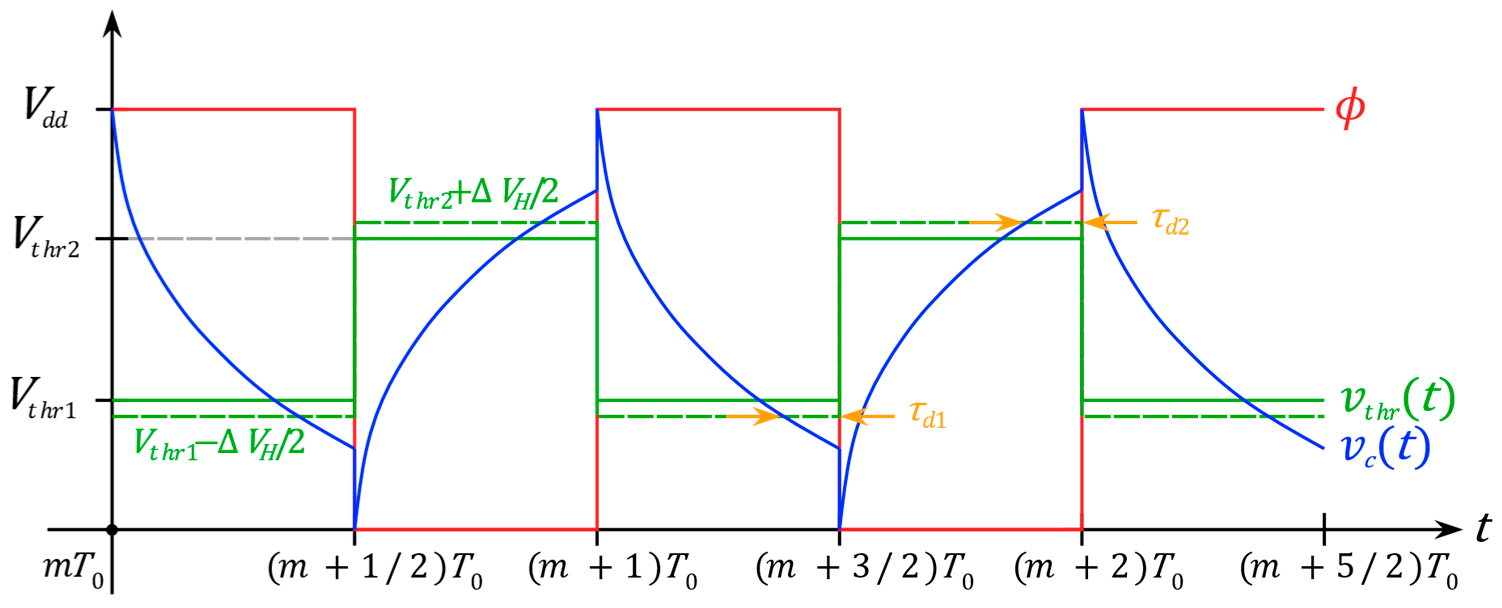
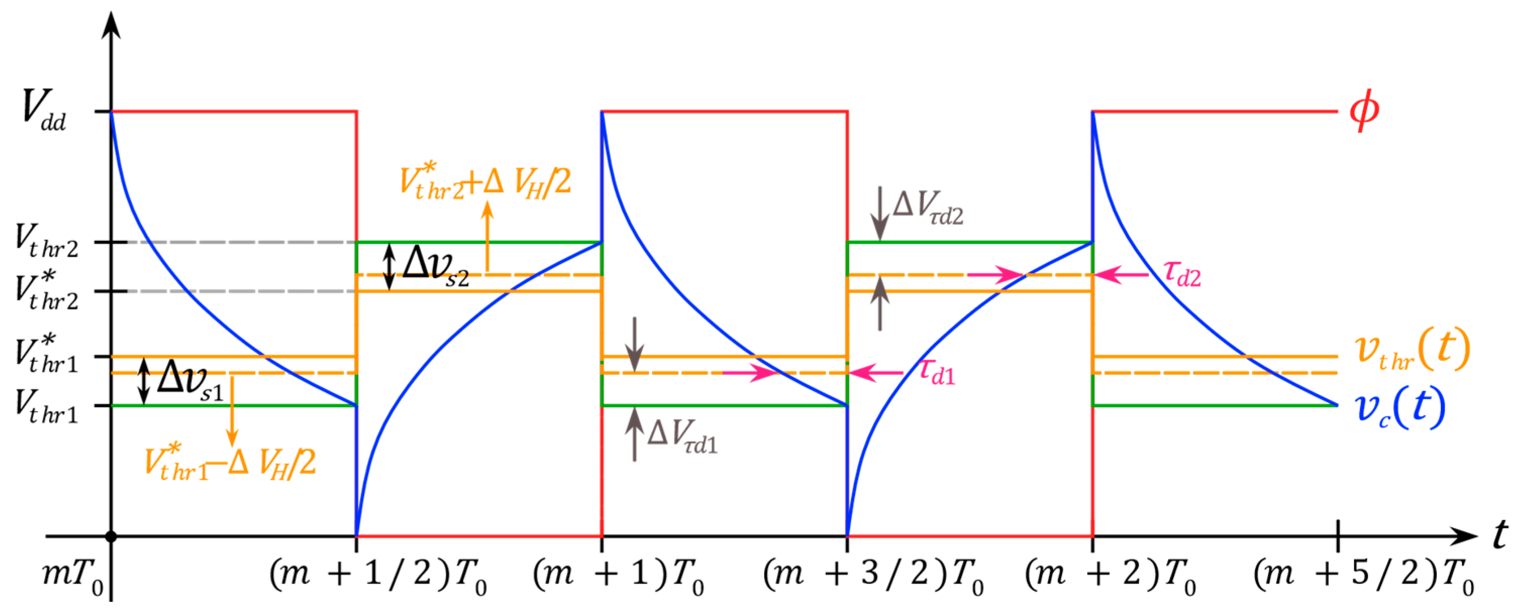
Figure 5 qualitatively shows the waveforms of relevant voltages in the circuit.
vc(
t) is the positive input voltage of the comparator, alternatively equal to either the voltage on the lower terminal of
C1 or the voltage on the upper terminal of
C2, depending on the output logic level. The effects of non-negligible comparator hysteresis and delay are also represented in the figure, as they are taken into account in the detailed analysis that follows.
A time-domain analytical treatment is first reported. Then, the maximum achievable FoM of the considered oscillator is assessed.
2.3.1. Time-Domain Analysis
The ideal oscillation period (e.g., neglecting all noise sources and all the comparator non-idealities) can be expressed as follows.
Again, α1 and α2 are the comparator thresholds normalized by Vdd, and the second equality is valid if α1 + α2 = 1, so that a 50% duty cycle is attained. The other equations present in this Section are also based on such a hypothesis.
In the following, the calculation of the real oscillation period is reported (e.g., discarding the simplification of an ideal comparator). A generic
m-th oscillation period is taken into account, beginning with a rising edge of the output waveform. Without any loss of generality, the considered oscillation cycle is assumed to start exactly at
t =
mT0. Equation (19) allows determining the
T1,m time interval needed for the
C1 capacitor voltage, decreasing from
Vdd to ground, to trigger a new switching event of the comparator, at the end of the first half-period. In other words,
T1,m is equal to the duration of the
clk = 1 phase, minus the comparator delay. In this equation, the approximation
T1,m ≅
T0/2 is performed in the arguments of the noise processes, implicitly neglecting second-order noise terms.
The left-hand side of Equation (19) represents the capacitor voltage at t = mT0 + T1,m, while the right-hand side consists of the effective comparator threshold. Three different noise contributions are present in Equation (19): the comparator threshold noise vn-comp(t), the RC-filtered thermal noise of the resistor vnc1(t), and the kT/C noise vε1[m], introduced at the beginning of the half-period because of the S1 switch opening. As for ΔVH, it indicates the width of the comparator hysteresis.
Through straightforward calculations hereby omitted, the real oscillation period
T0,m can be determined. First, Equation (19) has to be solved to find the time interval
T1,m; then, an analogous equation can be written for the subsequent half-period, allowing the time interval
T2,m to be calculated as well. Thereafter, recalling that the comparator thresholds are chosen to nominally attain a 50% duty cycle, the following relationship is achieved.
In this expression,
h Δ
VH/Vdd is the
Vdd-normalized hysteresis of the comparator and
τd1,
τd2 are the propagation delays of the high-to-low and low-to-high transitions of the comparator, respectively. As for the period jitter, a linear approximation is again possible, if we realistically assume all the noise samples to have standard deviations much smaller than
Vthr1. If, for simplicity, the approximation Δ
VH/2
Vthr1 is also carried out, the comparator and
kT/
C contributions to the period jitter can be expressed as follows:
The dual-slope oscillator of
Figure 4 is verified to apply standard CDS to the comparator noise. Through simple calculations, the comparator noise contribution to the period jitter PSD can be expressed as in Equation (12), with the topology-dependent coefficient being, in this case,
The minimum value
Gmin =
e2 ≅ 7.39 can be obtained by choosing
α1 =
α1,opt1 = 1/
e ≅ 0.368. This implies a reduction of
by almost a factor of three with respect to the elementary dual-slope
RC oscillator. This is accomplished thanks to two distinct effects. In the first place, the oscillator topology of
Figure 4 processes the comparator noise with standard CDS (rather than CTS). This results in a reduction of
Gmin, with respect to
GDC,min of the oscillator of
Figure 1b, by a factor of around 1.47, which is the ratio between the
Hs noise processing functions of CTS and CDS, both evaluated at
f = 0 for the optimum comparator threshold sizing. Moreover, the choice of widening the capacitor voltage swing is also helpful in decreasing the jitter statistics. It allows for a further reduction of
Gmin by a factor approximately equal to 1.84, which is the ratio between the
γcomp factors of the oscillators of
Figure 1b and
Figure 4, also evaluated for the optimum threshold sizing. The phase noise can be expected to improve roughly proportionally to the
G factor reduction, under the realistic assumption that the comparator noise still represents the main phase noise contributor.
2.3.2. Maximum Achievable FoM of the Dual-Capacitor Oscillator
As anticipated, the oscillator architecture of
Figure 4 implies a slight degradation of the maximum FoM. This happens because of the higher power needed to periodically charge the two capacitors (rather than just one capacitor) and because of the additional
kT/
C noise contributions
vε1,2[
m]. However, since the limit FoM worsens just moderately, the advantage of reducing the comparator noise contribution to the jitter is likely to be prevailing in a real design. Indeed, in standard relaxation oscillators, the comparator noise is known to be the dominant phase noise contributor close to the fundamental frequency. This is confirmed also by the simulation results reported in
Section 5, regarding a 0.18 µm CMOS implementation of the oscillator of
Figure 4.
To calculate the maximum achievable FoM, the variance of the kT/C contribution to the period jitter has to be determined first. The variance of the vnc1,2 noise samples, which represent the kT/C noise implied by the RC charging process of the capacitors, has to be accounted for by means of Equation (16), evaluated at t ≅ T0/2. As for the vε1,2[m] noise samples, introduced when the S1,2 switches open at the beginning of the half-periods, their variance can be considered simply as kT/C. To explain why this approximation holds, let us consider the capacitor being discharged through its related S1,2 switch, during a generic half-period. The switch is characterized by an Ron series resistance. Throughout the half-period, the variance of the noise voltage across the capacitor undergoes a very fast exponential transient towards kT/C, with a time constant equal to RonC RC. Thus, such an exponential trend reasonably reaches a value very close to kT/C by the end of the half-period. On the basis of these considerations, and assuming the comparator to be ideal and the duty cycle to be equal to 50%, the variance of the kT/C contribution to the period jitter can be easily expressed as in Equation (6). Through simple calculations, it can be shown that γkT/C(α1) = 2γcomp(α1) for the considered oscillator. Generally, for other relaxation oscillator topologies, a different relationship exists between these two coefficients.
The power needed to periodically charge the capacitors is given by Equation (24).
At this point, the FoM can be optimized with respect to
α1. In the following,
fom refers to the figure of merit expressed on a linear scale. Combining Equations (1) and (17), it can be expressed as follows.
Again, an optimum sizing of the comparator thresholds can be found: the
F(
α1) coefficient is minimized (and, hence, the FoM is maximized) for
α1 =
α1,opt2 ≅ 0.525. It can be noticed that such an optimum value is different from α
1,opt1 ≅ 0.368, which minimizes the comparator-related period jitter component. Depending on which jitter component prevails between the comparator-related and
kT/
C-related ones, a different optimum sizing should be chosen. Opting for α
1 = α
1,opt2 results in
Fmin ≅ 4.15 and FoM ≅ 167.6 dBc/Hz. Thus, the maximum achievable FoM slightly worsens with respect to the basic dual-slope
RC oscillator (by 1.4 dBc/Hz). Nevertheless, such a loss is surely acceptable if we consider that, in most design cases, the comparator noise actually represents the main phase noise source. On the other hand, as previously argued, the oscillator topology of
Figure 4 offers an appreciable improvement regarding the jitter component related to the comparator noise, thanks to the standard CDS being applied rather than CTS.
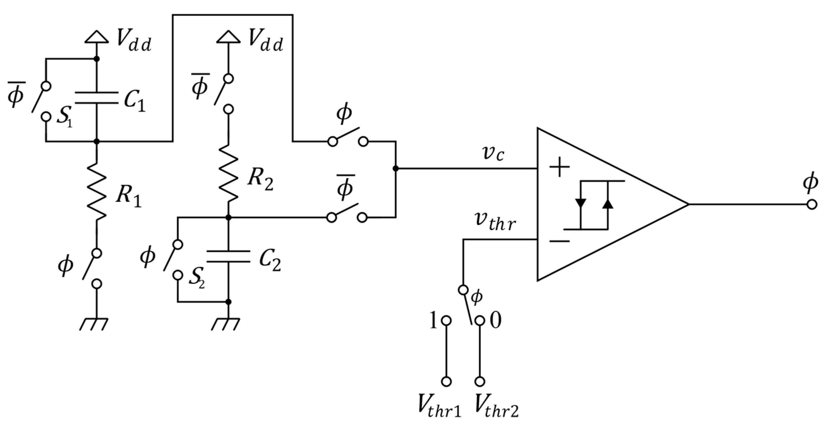
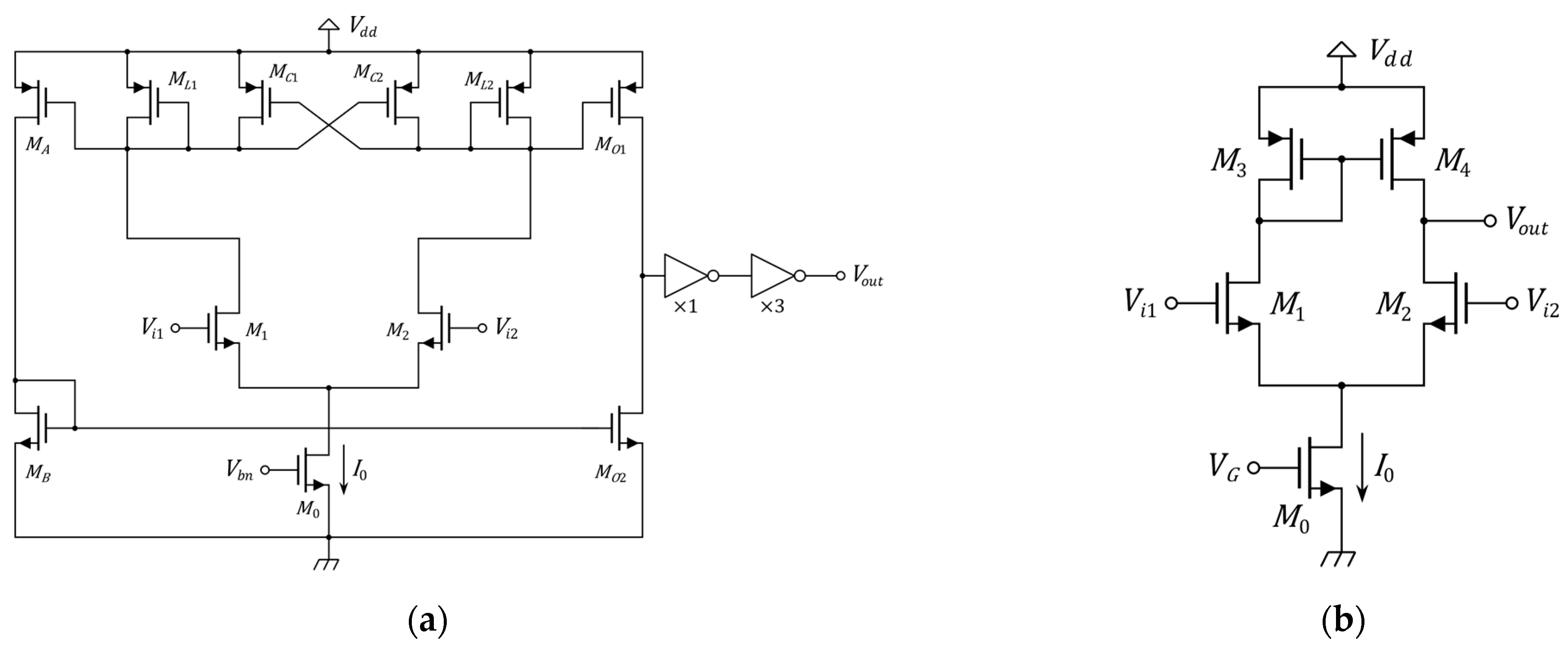
3. Proposed Architecture
As illustrated in
Section 5 by means of simulation results, the dual-capacitor
RC oscillator of
Figure 4, while representing an improvement with respect to the simple topology of
Figure 1b, still has its phase noise dominated by the comparator noise. In this paragraph, the novel CSTA approach for the rejection of the comparator-related phase noise is presented, aiming at further improving the close-in phase noise and the long-term accumulated jitter. The operating principle is first described, followed by an analytical treatment clarifying its beneficial effect on the jitter and the phase noise.
The proposed technique compensates the comparator-related oscillation period error by means of a discrete-time self-adjustment of the comparator thresholds. It exploits the fact that, at switching instants, the
vc(
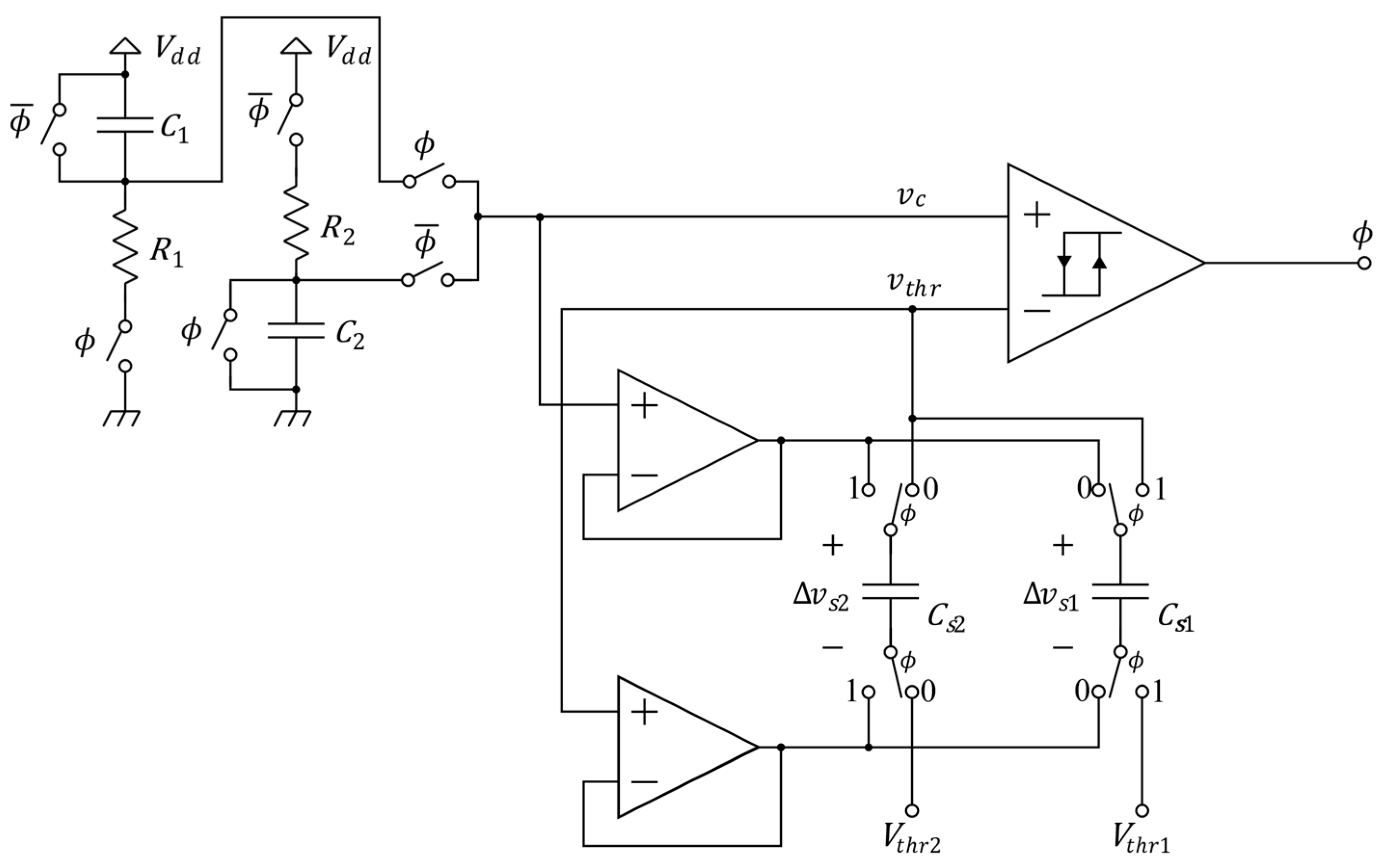
t) voltage actually differs from the comparator threshold because of the comparator hysteresis, delay, and noise. In the proposed oscillator, such a threshold error is sampled and used to properly adjust the comparator threshold of the subsequent half-period. Therefore, the period error due to the comparator hysteresis and delay is canceled out and the comparator threshold noise is processed through a more effective CDS variant, not presenting any noise fold-over at low frequencies. The proposed architecture is shown in
Figure 6, while the qualitative waveforms of relevant signals are represented in
Figure 7 (in steady-state conditions). In
Figure 7, the corrected thresholds are indicated with
and
.
In order to implement the above-mentioned approach, the CS1,2 capacitors complementarily undergo two working phases, each coincident with a half-period of the oscillation: a tracking phase of the comparator differential input voltage and a holding phase of the sampled threshold error. During the latter, the sampled error is employed to dynamically correct the new comparator threshold. Two buffers are needed to avoid any unwanted charge redistribution between the main capacitors and the sampling ones.
Here follows a brief analysis to better illustrate the effectiveness of the proposed technique against the comparator noise. Subsequently, the maximum achievable FoM of the CSTA-compensated oscillator is also assessed.
3.1. Time-Domain Analysis of the CSTA Oscillator
Since the oscillator core is the same as
Figure 4, the ideal oscillation period is still given by Equation (18). However, to calculate the real oscillation period, the effective comparator thresholds can be expressed as in Equation (27), to account for their dynamic adjustment.
The correction terms, obtained by sampling the threshold errors, are indicated by Δ
vs1,2[
m]. They can be expressed as follows.
The threshold error sampled at the end of a given half-period, used to correct the threshold of the subsequent half-period, accounts for the comparator hysteresis and delay, the comparator noise
vn-comp, and the
kT/
C noise
vnc1,2 due to the charging process of the main capacitor. The Δ
Vτd1,2 terms are the overshoots of
vc(
t) due to the comparator propagation delays. The presence of comparator noise samples in the correction terms Δ
vs1,2[
m] gives rise to the effective comparator-noise-processing mechanism offered by the CSTA technique. However, unwanted noise terms
vns1,2[
m] are unavoidably added as well, as a consequence of the track and sample approach. They are composed of two distinct contributions, as made clear by Equation (30): the output noise of the buffers
vnb-A,B(
t) and the
kT/
C noise
vεs1,2[
m] implied by the sampling operations.
In Equation (30), generically expressing both the vns1[m] and vns2[m] terms appearing in Equations (28) and (29), the employed convention is tm1 = mT0 and tm2 = mT0 + T0/2.
The real oscillation period
T0,m can now be calculated, following the same steps of
Section 2.3.1. To this purpose, equations analogous to Equation (19) can be solved to determine the half-period durations, with the corrected thresholds
[
m] taking the place of the uncompensated thresholds
Vthr1,2. The following expression of the oscillation period can ultimately be achieved. Again, the choice
α1 +
α2 = 1 is made, to impose the 50% duty cycle.
The hysteresis-related error is exactly canceled out. A partial compensation of the delays also occurs, thanks to the second term of Equation (31) being negative. In actuality, under the simplifying hypothesis of equal high-to-low and low-to-high propagation delays of the comparator output voltage (
τd1 and
τd2, respectively), and assuming the feedback compensation technique has reached its steady state, the compensation would be exact. Indeed, it can be shown that, under these hypotheses, both the overshoots due to the comparator delays result to be equal to
where we assume
τd1 ≅
τd2 ≅
τd and Δ
Vτd1 ≅ Δ
Vτd2 ≅ Δ
Vτd.
As for the period jitter, it can be approximately expressed as the summation of the contributions from the comparator, thermal noise (
kT/
C), and from the buffers, given by Equations (33)–(35), respectively:
The comparator threshold noise is processed through CDS employing noise samples separated by a full oscillation period, as indicated in Equation (33), rather than a half-period. From here on, this CDS variant will be referred to as
T0-CDS. It can be demonstrated that, for
T0-CDS, the noise-shaping function appearing in the PSD of the resulting effective noise, in Equation (4), is given by the following expression.
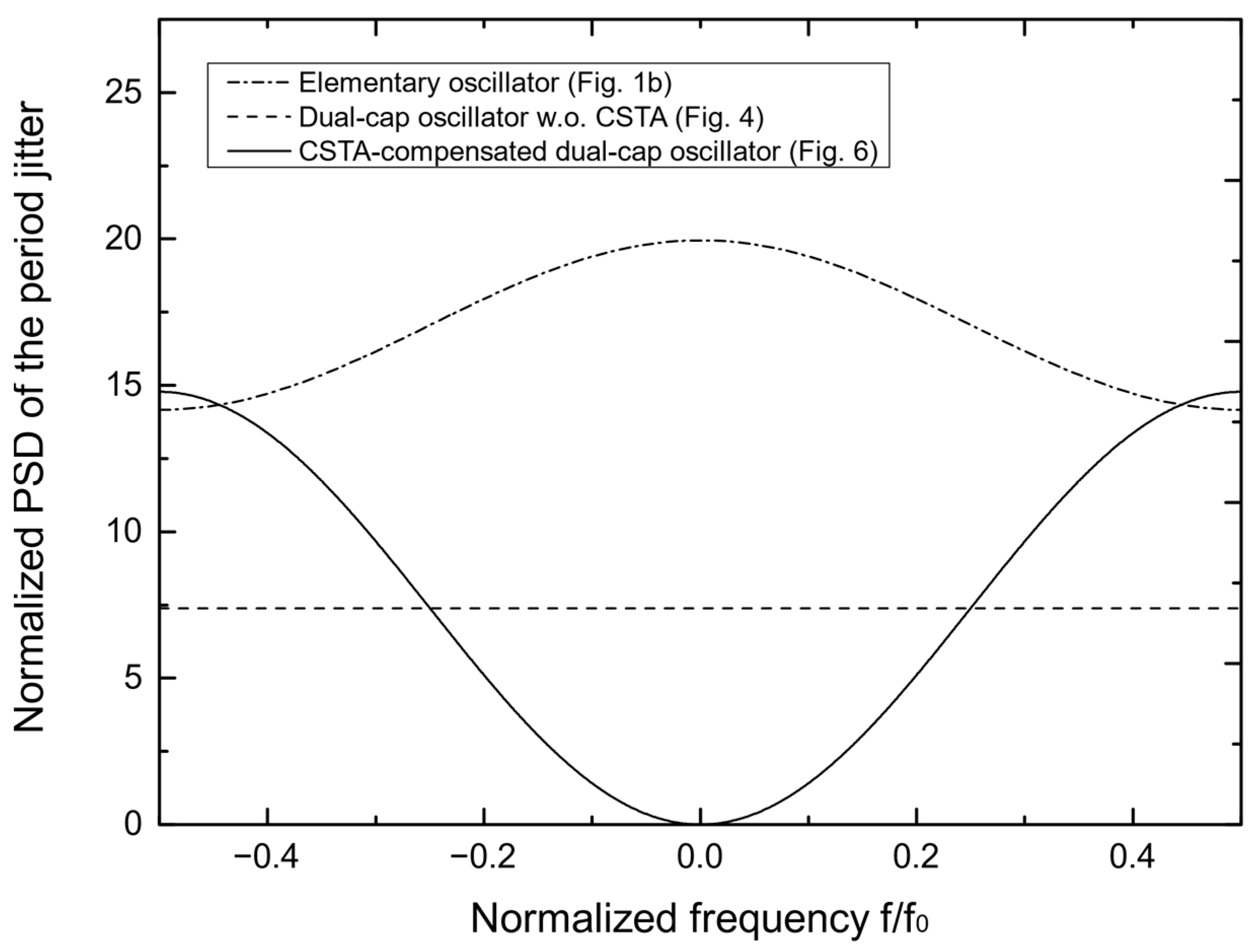
Therefore, as a consequence of the feedback-based compensation, the comparator contribution
to the period jitter PSD results to be negligible at low frequencies. As illustrated by
Figure 8, no noise fold-over occurs at low frequencies. This is achieved at the cost of a doubled fold-over at high frequencies with respect to the traditional CDS. However, the high-frequency components of the period jitter PSD translate into far-out phase noise, which is the cause for the short-term accumulated jitter. As previously argued, the long-term accumulated jitter is actually way more critical for many relaxation oscillator applications; thus, the just-mentioned trade-off between the close-in and far-out phase noise is ultimately beneficial.
The
γcomp(
α1) topology-dependent coefficient is still the same as the uncompensated oscillator of
Figure 4, hence
is again optimized by the choice
α1,opt1 = 1/
e ≅ 0.368.
Figure 8 shows a comparison amongst the
G(
f) coefficients, shaping the
PSDs of the three oscillators that were analyzed. The
G(
f) coefficients are defined according to Equation (14) and evaluated for the optimum sizing of the comparator thresholds.
Summarizing, the proposed compensation approach is able to prevent the comparator noise from contributing to the close-in phase noise. On the other hand, the output noise of the buffers gives rise to an additional jitter contribution. However, this was verified not to represent a much detrimental issue, as we quantitively show in the noise summary reported in
Section 5. The standard CDS is applied to the buffers’ noise, in Equation (35), and, as suggested by the just-anticipated simulation results, the resulting effective noise does not affect the phase noise significantly, even though the low-frequency noise fold-over, in this case, still occurs. It may be argued that, for the buffers, the condition on the flicker corner frequency being low enough might be easier to meet with respect to the case of the comparator, hence ensuring a better efficiency of the CDS processing. In fact, to obtain reasonably low propagation delays, the comparator should be designed with almost minimum-area transistors, to benefit from fast device turn-on and switch-off transients. However, minimizing the gate areas implies large flicker noise contributions [
32], thus causing a high flicker corner frequency of the comparator noise. On the other hand, transistors with larger areas can be employed in the buffers, because their speed requirements are more relaxed. Indeed, concerning the buffers, the only requirement is that their settling time is shorter than the half-period duration, since the sampling of the threshold error occurs only at the end of the considered half-period.
3.2. Maximum Achievable FoM of the CSTA Oscillator
Seemingly, a downside of the proposed approach lies in the increase of the kT/C noise contributing to the period jitter; namely, the vεs1,2[m] noise samples are introduced in Equation (34), as a consequence of the CSTA compensation based on a track and hold mechanism. However, concerning real design cases, the limit FoM decrease (with respect to the reference value of 169 dBc/Hz) is certainly not invalidating.
To quantify the reduction of the limit FoM, the same steps of
Section 2.3.2 can be followed. Because of the additional
vεs1,2[
m] noise terms, whose variance can be considered equal to
kT/
C, the
γkT/C(
α1) factor results to be doubled with respect to the uncompensated dual-capacitor
RC oscillator (
Figure 4). If we still consider the power consumption to be ideally due only to the charging of the main capacitors, the maximum FoM is found by optimizing the following quantity, appearing in the relationship
fom =
F(
α1)
kT.
Choosing
α1,opt2 ≅ 0.525 allows achieving
Fmin ≅ 8.3. The resulting figure of merit is FoM ≅ 164.6 dBc/Hz, which is actually close to the maximum FoM achievable by ring oscillators and I-C relaxation oscillators [
15,
22].
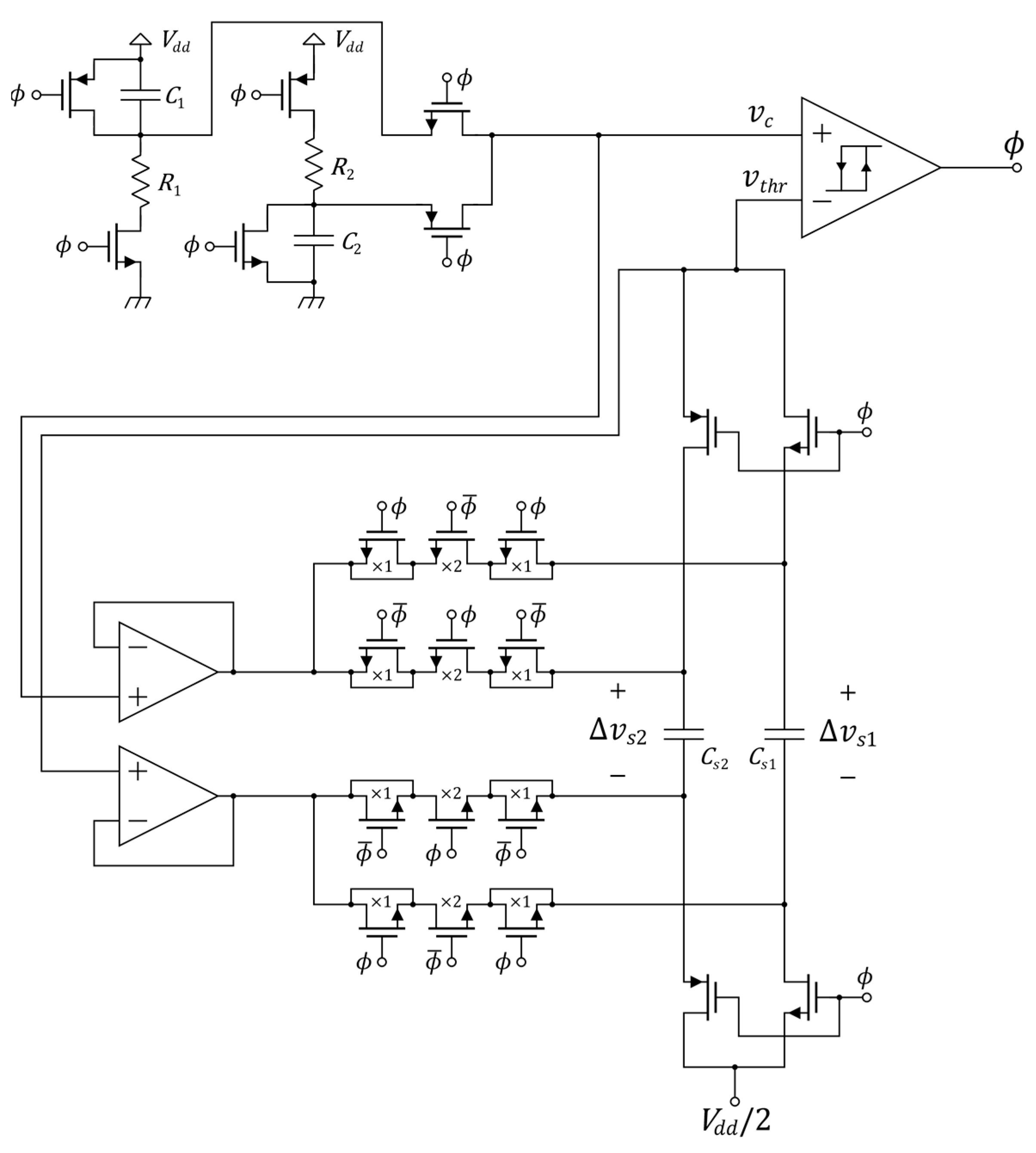
4. Transistor-Level Implementation
In this section, we describe a transistor-level design of the proposed CSTA-compensated
RC oscillator for a 10 MHz oscillation frequency. The target process is the 0.18 μm–1.8 V CMOS process by UMC.
Figure 9 shows the transistor-level schematic view of the circuit.
For the comparator, a very common topology based on a four-transistor hysteresis cell was employed (
Figure 10a), able to produce full output logic levels (0,
Vdd). The transistors of the hysteresis cell were sized as follows:
ML1 =
ML2 with
WL = 800 nm,
L = 800 nm, and
MC1 =
MC2 with
WC = 1.2 μm, L = 800 nm. Such design choices allowed for a good compromise between the comparator delay (it can be verified that it would be minimized by sizing the comparator MOSFETs with minimum areas) and the flicker component of the threshold noise (which decreases with increasing areas [
32]). The tail current was set to 2.4 μA and the input transistors were sized with
W/
L = 3, resulting in a hysteresis width equal to Δ
VH = 36 mV. The two inverters cascaded to the comparator, sized with scaling-up transistor widths, allow for a higher driving strength of capacitive loads [
33].
The buffers involved in the CSTA compensation were implemented with simple single-stage amplifiers (
Figure 10b). The tail currents were set to 12 μA, to achieve a high enough tracking speed. The transistors of the input pair were sized with
W/
L = 4, resulting in a moderate inversion bias, while their areas were chosen large enough to make the flicker corner frequency sufficiently smaller than the oscillation frequency.
Another aspect worth mentioning is that, rather than alternating between two distinct comparator thresholds half-period by half-period, we opted for employing equal comparator thresholds Vthr1 = Vthr2 = Vdd/2 (α1 = α2 = 0.5). With such a choice, α1 is close to the optimum value (α1,opt2 ≅ 0.525) that minimizes the kT/C contribution to the jitter, while the architecture is significantly simplified.
The passive devices were sized as follows: R1 = R2 = 214 kΩ, C1 = C2 = 250 fF, and CS1 = CS2 = 80 fF. All the capacitors are metal–insulator–metal (MIM) capacitors, and the resistors are polysilicon resistors. Relatively small values were chosen for the sampling capacitors CS1,2 to allow for a sufficiently high tracking speed by the buffers. To minimize sampling errors due to charge injection, the switches of the compensation sub-circuit were equipped with dummy switches.
5. Simulation Results
We designed a prototype of the proposed oscillator with the Cadence Virtuoso Platform for Custom IC design. Then, performances of the design were assessed through accurate electrical simulations, performed by means of the Spectre simulator. The obtained results are reported in this section, with a particular focus on the phase noise and jitter performances. Comparisons between the uncompensated
RC oscillator of
Figure 4 and the
RC oscillator equipped with the novel compensation technique are proposed.
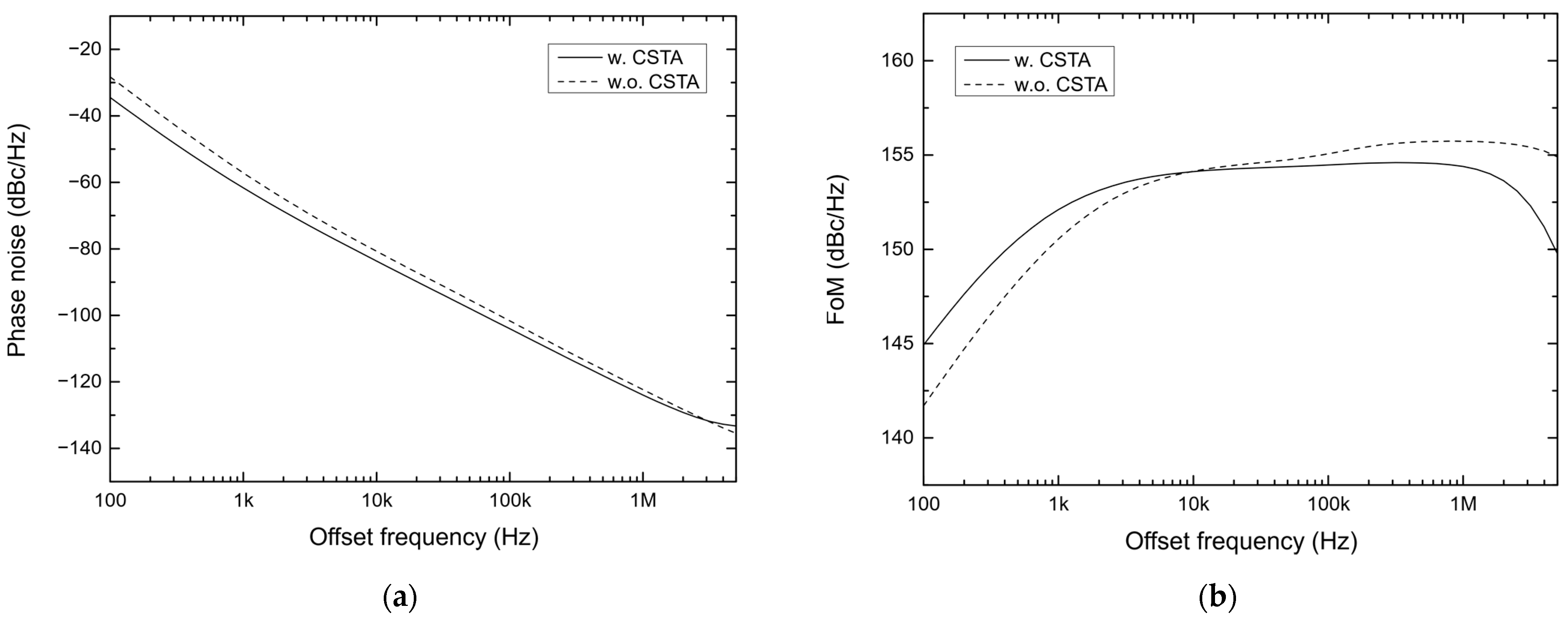
Figure 11a shows the simulated phase noise spectrum, and relevant data related to it are reported in
Table 1. The compensation technique effectively decreases the phase noise at frequencies close to the carrier. As a matter of fact, at a 100 Hz offset frequency, an improvement of more than 6 dB/Hz is accomplished. At frequencies farther from the carrier, a reduction of the phase noise can still be noticed, even though it is much less appreciable. Such a behavior is consistent with the previously presented jitter model: the proposed compensation mechanism is effective in reducing the comparator-related close-in phase noise, thanks to the particular CDS-like processing it applies. However, it also implies an increased fold-over of the comparator noise itself at higher frequencies, while additional white noise sources are also introduced.
Regarding the figure of merit, the phase noise reduction is partially traded-off with the increased power consumption, mainly due to the buffers. Still, at a 100 Hz offset frequency, a FoM improvement of 2.5 dB/Hz can be noticed. On the other hand, a degradation of the FoM at offset frequencies higher than 10 kHz also occurs. That is because, as it was just recalled, the proposed approach is effective mostly against the close-in phase noise, while at far-out frequencies the FoM happens to be mainly affected by the increased consumption.
Delving more into detail about the effects of the CSTA compensation,
Table 2 presents a noise summary of the individual phase noise contributions, evaluated at a 1 kHz offset frequency. In particular, a close focus on the contribution from the comparator noise is proposed. In the uncompensated oscillator of
Figure 4, despite the standard CDS being applied, the comparator-related phase noise represents 81.9% of the overall phase noise. As shown in the reported noise summary, this is mainly due to the flicker comparator noise. This flicker contribution is likely to be folded over as well by CDS, as a consequence of the insufficiently low flicker corner frequency. Such an issue could not be prevented without unacceptably worsening the comparator propagation delays.
The CSTA compensation technique turns out to be effective against the comparator noise. Indeed, its phase noise contribution results to be decreased by a factor almost equal to 7. The impact of the buffers’ output noise on the phase noise is also moderate. In conclusion, considering the FoM evaluated at 1 kHz, its 12.6 dB/Hz difference with respect to the maximum achievable value of 164.6 dBc/Hz (
Section 3.2) is mainly due to the increased consumption (10.5 dB/Hz), while only 2.1 dB/Hz are lost because of sub-optimal phase noise. This means that an almost minimum close-in phase noise has been achieved.
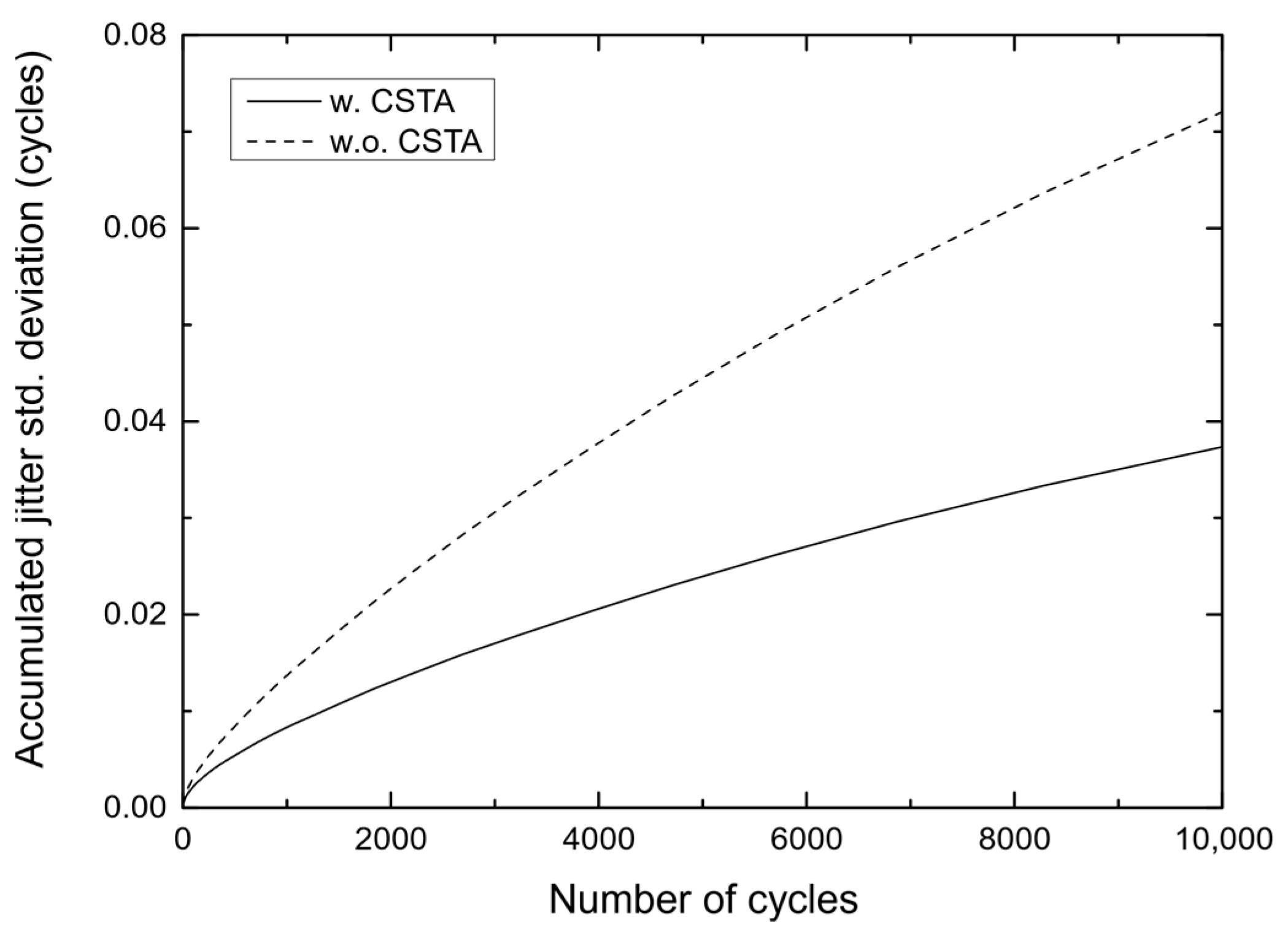
Figure 12 characterizes the jitter accumulation phenomenon, representing the standard deviation of the accumulated jitter as a function of the number of observed oscillation cycles. The CSTA-compensated oscillator presents a remarkable reduction of the jitter accumulated in the medium/long term (throughout 10k oscillation periods, the standard deviation of the accumulated jitter results to be lower than 4 ns).
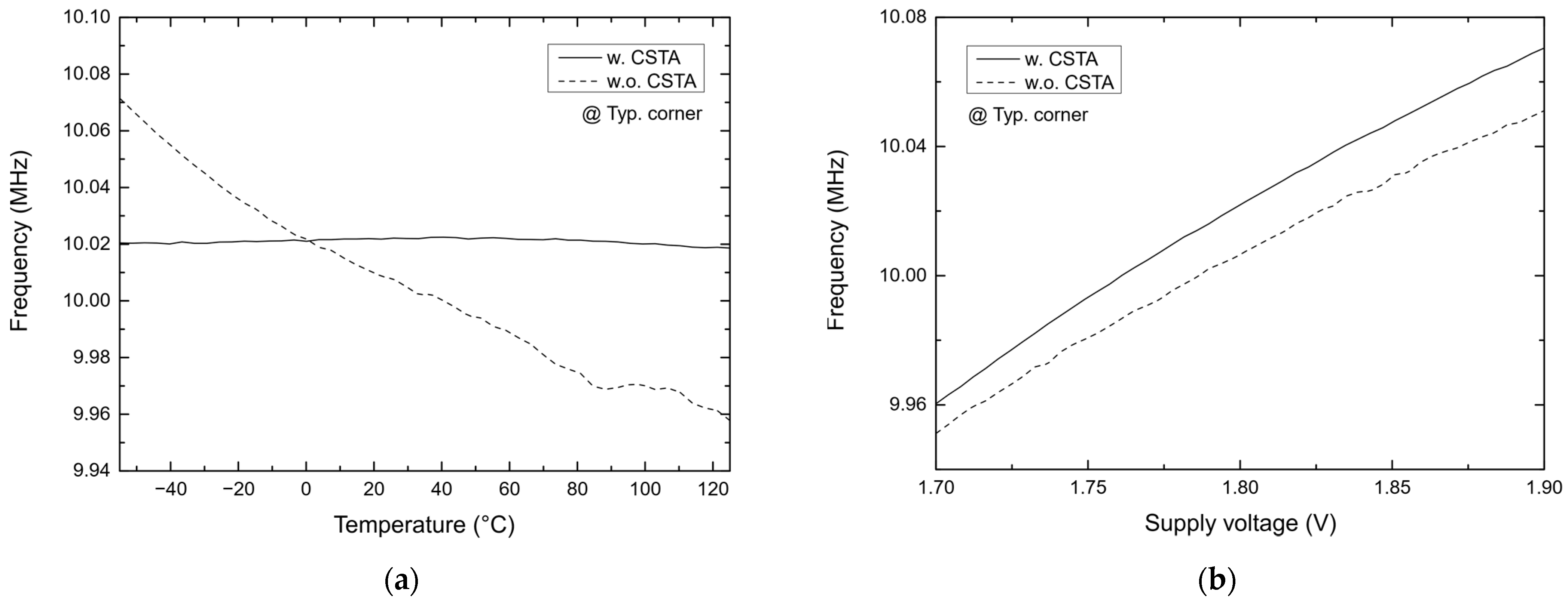
Even though, so far, we concentrated mostly on the phase noise and jitter performances, we also characterized the PVT sensitivity of the oscillation frequency. As already mentioned, RC relaxation oscillators cannot be expected to present valuable performances under this viewpoint. This is particularly true for the case of the process sensitivity, mainly due to the typically large spread affecting integrated resistors.
In the following, we first present results regarding the VT-sensitivity. Referring to the typical process corner,
Figure 13a,b show the oscillation frequency as a function of temperature and of the supply voltage, respectively.
We assessed the VT-sensitivity also in different process corners, and the resulting data are reported in
Table 3. In particular, as for the temperature sensitivity, the temperature coefficients (TCs) were calculated within the full military temperature range (−55,125) °C, according to the following definition:
where
Tnom is the room temperature (27 °C). The supply voltage coefficients (SVCs) were estimated analogously, as indicated by Equation (39), referring to a (1.7,1.9) V
Vdd range.
In this relationship, Vdd,nom = 1.8 V, as nominally required by the employed 0.18 µm CMOS process.
A competitive temperature sensitivity is attained at all the process corners. Indeed, when the CSTA compensation technique is employed, the maximum absolute value of the TC across all the considered process corners results to be approximately equal to 20 ppm/°C. It was possible to achieve such a result thanks to the fact that resistors with a negative temperature coefficient (NTC) were used in the design. The observed TC is actually the result of partial compensation between the resistor TC and the temperature dependency of the comparator and logic gate delays. The latter prevails (negative TC of the frequency) for the uncompensated oscillator, while a far better compensation appears for the CSTA oscillator. This happens because the CSTA approach is able to mitigate the effects of the comparator delays, which, as already argued, feature the strongest temperature dependency amongst the terms determining the duration of the real oscillation period. In particular, the good results reported for the oscillation frequency TC arise from a better compensation between the temperature dependencies of the resistors and of the comparator delay residues. As shown in
Table 3, the attained TC also results to be reasonably robust with respect to process variations.
As for the sensitivity to the supply voltage, the uncompensated and CSTA oscillators present a quite similar performance, with a voltage sensitivity around 5%/V.
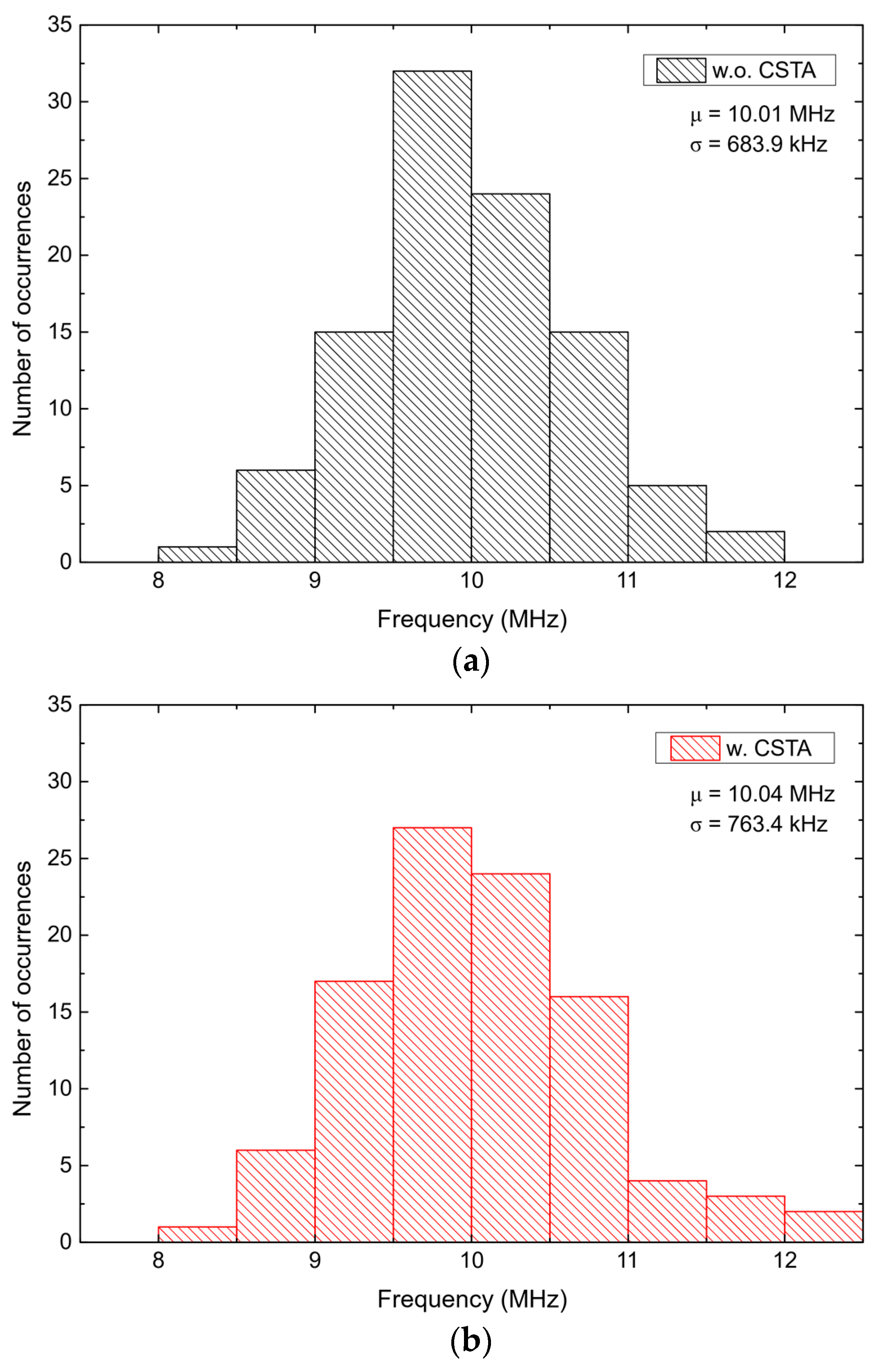
The process sensitivity is also not improved by the proposed approach. We performed 100 Monte Carlo runs for both the uncompensated and the CSTA-compensated oscillators, including both global and local (mismatch) process errors.
Figure 14a,b show the resulting histograms, characterizing the process spread of the oscillation frequency for the basic oscillator and the compensated one, respectively.
To conclude, a performance comparison with state-of-the-art relaxation oscillators is presented in
Table 4. In addition to the previously defined parameters, the power-efficiency figure of merit is also reported, defined as FoM2 =
P/
f0 (µW/MHz).
It is worth noticing that, concerning the FoM evaluated at a low offset frequency (1 kHz), our proposed solution achieves a competitive result in the comparison with state-of-the-art relaxation oscillators, thanks to the CSTA technique effectively reducing the phase noise component related to the comparator flicker noise. SB-based solutions, such as [
16,
17], indeed allow for lower phase noise; nonetheless, as already argued, they might be uncompliant with standard n-well CMOS processes. The temperature sensitivity accomplished in this work is also remarkably low with respect to the other works reported in
Table 4.


 ,
, 


