Abstract
The FinFET architecture has attracted growing attention over the last two decades since its invention, owing to the good control of the gate electrode over the conductive channel leading to a high immunity from short-channel effects (SCEs). In order to contribute to the advancement of this rapidly expanding technology, a 3D 14-nm SOI n-FinFET is performed and calibrated to the experimental data from IBM by using Silvaco TCAD tools. The calibrated TCAD model is then investigated to analyze the impact of changing the fin width, fin height, gate dielectric material, and gate length on the DC and RF parameters. The achieved results allow gaining a better understanding and a deeper insight into the effects of varying the physical dimensions and materials on the device performance, thereby enabling the fabrication of a device tailored to the given constraints and requirements. After analyzing the optimal values from different changes, a new device configuration is proposed, which shows a good improvement in electrical characteristics.
1. Introduction
The structure of the fin field-effect transistor (FinFET) has completely emerged as a promising design solution for CMOS logic and memory circuit design because of its good immunity to short channel effects (SCEs) [1,2,3]. This technology enables the creation of high-performance ultra-scaled, high-density integration, and high-performance silicon (Si) chips [1,2,3,4]. In the silicon industry, device miniaturization is still considered a key feature to achieve better short-channel performance. Currently, a great effort concerns the development of FinFET devices with dimensions below 5 nm that represent the target in the near future [4,5,6,7,8]. Despite the effort made to create devices with dimensions below 5 nm, many aspects still remain to be clarified and optimized, also with a view to a larger-scale application of the devices.
This paper presents an investigation of 3D 14-nm FinFET on thin silicon on insulator (SOI) wafer using Silvaco tools. The SOI technology shows significantly large improvement compared to the previous FinFET technology. For better Si channel controllability, hafnium oxide (HfO2) was used to cover the Si channel as a gate dielectric. The impact of varying the fin width (Wfin = 4, 6.5, 15, and 20 nm), fin height (Hfin = 10, 15, 20, 25, 30, and 35 nm), gate dielectric materials (TiO2, La2O3, HfO2, Al2O3, Si3N4, and SiO2), and gate length (Lg = 5, 10, 15, and 20 nm) on the DC and RF performance of the considered structure is carefully analyzed and discussed. The analysis is performed by investigating the following parameters: threshold voltage (Vth), subthreshold slope (SS), drain-induced barrier lowering (DIBL), on-state current (Ion), off-state current (Ioff), Ion/Ioff ratio, transconductance (gm), gate capacitance (Cgg), and cut-off frequency (fT). The development of a comparative analysis enables gaining a better understanding of how to improve device performance, depending on the given fabrication constraints and application requirements.
It should be underlined that the great interest in the FinFET technology is witnessed by the many papers that have been published over the years to investigate the FinFET performance by using both TCAD simulations [8,9,10,11,12,13] and measurements [14,15,16,17,18]. Although a measurement-based investigation is a mandatory step prior to the use of a device in real applications, the TCAD simulation is considered a powerful and costless type of analysis to optimize device performance. This is because the TCAD tool allows predicting how the device performance changes by varying the design parameters without the need for time-consuming and costly experiments [13].
2. Device Structure
The 3D 14-nm SOI FinFET device has been simulated using Silvaco TCAD. Figure 1 shows the 3D schematic diagram of the FinFET device with a physical gate length (Lg) of 20 nm. The geometrical parameters and material properties are specified in previously published papers [1,2,3]. HfO2 is used as a gate dielectric material. The doping densities of the source (n-type), drain (n-type), and covered fin (p-type) region were 1 × 1021 cm−3, 1 × 1021 cm−3, and 1 × 1016 cm−3, respectively. The contact resistance of 1 × 10⁻⁹ Ω.cm2 was selected for the source/drain region. Table 1 illustrates the physical parameters of the investigated model.
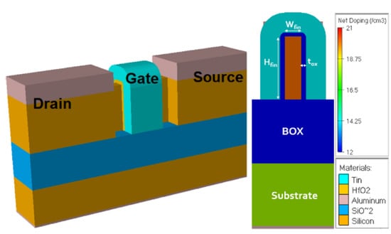
Figure 1.
Structure of 3D 14-nm SOI n-FinFET device with a single fin.

Table 1.
Device parameters for a 14-nm n-FinFET.
3. Simulation Model
For device simulation, CVT, CCSMOB, ANALYTIC, BGN, SRH, and Auger recombination were also included. Fermi–Dirac distribution has been enabled. For quantum confinement, the BQP model was considered [13]. By considering a FinFET device based on using one single fin, the effective channel width can be estimated as follows
where Hfin is the fin height and Wfin is the fin width.
Weff = 2Hfin + Wfin
The electron (n) and hole (p) densities with BQP equation can be expressed by [13]
Nc and Nv are the effective density of states for electrons and holes, respectively. Ec and Ev are the conduction and valence bands, respectively. k is the Boltzmann constant, TL is the local lattice temperature, q is the electric charge, Q is the quantum potential, M−1 is the inverse effective mass tensor, and γ and α are two adjustable parameters.
Device Validation
Initially, the investigated 14-nm SOI n-FinFET model was carefully calibrated according to the experimental data in [1]. In order to match the simulated I–V curves with the experimental data from IBM [1], some physical parameters such as the doping density, thickness, source/drain extension length, and gate work function were carefully adjusted. Figure 2 illustrates simulated I–V characteristics at two different values of Vds: 0.05 V (linear) and 0.8 V (saturation). I–V model curves exactly match with the experimental as is observed at both bias conditions. The device characteristics of the investigated model are compared to the experimental outputs [1] and presented in Table 2. To further validate the developed model, the simulation results were compared also to Sun’s work [2]. Figure 3 presents the output I–V characteristics of the investigated model at different gate-source voltages. Figure 3 shows a non-zero current for Vgs just above Vth and the increase in Ids with increasing input voltage Vgs.
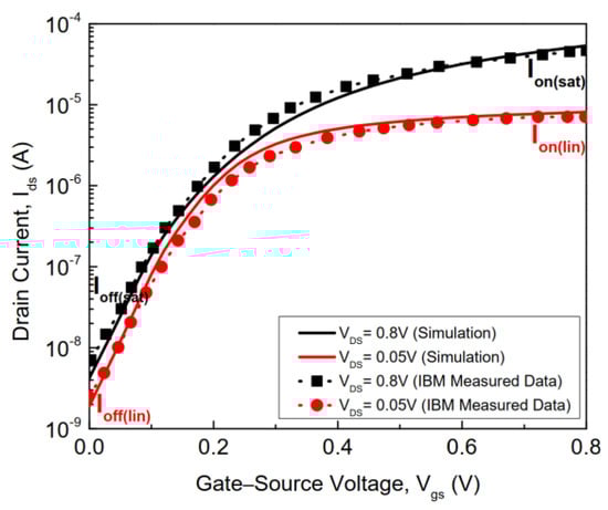
Figure 2.
Simulation and experimental I–V curves of the investigated FinFET model [1].
Table 2.
Characteristics for the investigated FinFET model.
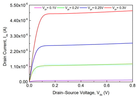
Figure 3.
Output I–V curves of the investigated FinFET model with different gate–source voltages.
To evaluate the SCEs, the subthreshold slope (SS) and drain-induced barrier lowering (DIBL) are extracted as follows [4,11]
where Vgs is the gate-source voltage and Ids,sat is the drain current (under saturated biasing condition). Vth,sat and Vth,lin are the threshold voltages under saturated and linear conditions, respectively. The values of SS and DIBL are, respectively, 61 mV/dec and 43.32 mV/V for the 14-nm n-FinFET. These parameters are approximately maintained the same as the ones reported in papers [1,2,3,4].
The cut-off frequency (fT) is considered as a crucial RF parameter which defines the speed response of the RF circuit design. The fT can be expressed by [14,15,16,17]
where gm is the transconductance, Cgg is the total gate capacitance, Cgs is the gate-source capacitance, and Cgd is the gate-drain capacitance.
4. Results and Discussion
In this section, the effects of changing the fin width, the fin height, the gate dielectric material, and the gate length on the device performance are analyzed and investigated for the SOI FinFET structure under study. The investigated tri-gate FinFET device has a 3D channel as illustrated in Figure 1. The model was calibrated with an agreement to IBM’s model (see Figure 2). The electrical characteristics of the FinFET device are evaluated at a room temperature of 300 K.
4.1. Effects of the Fin Width/Height on Device Performance
In this study, it is important to start by investigating the effect of different fin size ratios on device characteristics. To analyze the impact of the fin width on the device performance, the fin width of the studied structure was varied from 4 nm to 20 nm with the fin height kept fixed at 26 nm. It should be underlined that, although a larger fin width allows enlarging the total gate width (see Equation (1)), when the gate length shrinks, the Wfin width has to shrink as well in order to maintain an efficient suppression of the SCEs [19]. Figure 4 reports the effect of changing the fin width on the transfer I–V characteristics and the corresponding transconductance (Triangle symbols) for the investigated device. As can be clearly observed, the increase in the fin width leads to a reduction of the threshold voltage, in agreement with what is expected from previous studies [18]. In addition, owing to the increase of the total gate width (see Equation (1)), a larger fin width implies an increase in the drain current and transconductance [9,18]. Figure 5 shows the total gate capacitance versus Vgs for the studied device with different values of the fin width. As can be seen, as Vgs increases, Cgg increases until its value becomes roughly constant [4]. The value of Cgg decreases by decreasing the fin width, due to the reduction of the total gate width. Figure 6 shows fT variation as a function of Vgs for the studied device with different values of the fin width. The peak in fT increases as Wfin reduces. The behavior of fT is mainly due to the impact of the fin width on Cgg rather than on gm, as can be observed from Figure 4, Figure 5 and Figure 6. The peak point of fT is 3.9 THz at Vgs = 0.21 V with a Vds = 0.05 V for a device with a fin width of 4 nm.
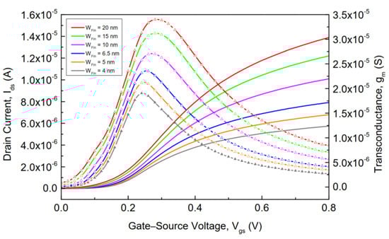
Figure 4.
Behavior of the drain current (left axis) and transconductance (Triangle symbols, right axis) versus the gate–source voltage with different values of the fin width at Vds = 0.05 V. The fin height is kept fixed at 26 nm.
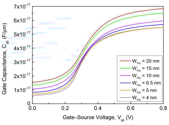
Figure 5.
Gate capacitance as a function of gate–source voltage with different values of the fin width at Vds = 0.05 V. The fin height is kept fixed at 26 nm.
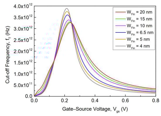
Figure 6.
Cut-off frequency as a function of gate–source voltage with different values of the fin width at Vds = 0.05 V. The fin height is kept fixed at 26 nm.
The variations of the threshold voltage, subthreshold slope, on-current, and off-current with different values of the fin height (Hfin = 10, 15, 20, 25, 30, and 35 nm) and of the fin width (Wfin = 4, 6.5, 15, and 20 nm) are shown in Figure 7, Figure 8, Figure 9 and Figure 10, respectively. Figure 7 shows a reduction in the threshold voltage with increasing Hfin and/or Wfin. Figure 8 shows the impact of Hfin on the subthreshold slope for FinFET devices with different values of Wfin at Vds = 0.05 V. This figure shows a slight impact of changing Hfin on SS when considering the lower values of the fin width (i.e., 6.5 nm and 4 nm), whereas a marked increase in SS is observed with increasing Hfin and/or Wfin when considering higher values of the fin width. It was observed that, for the studied FinFETs, a smaller fin width leads to better device performance in terms of SS. This confirms that studying the impact of varying fin width and fin height is essential for enabling technology development, since they can have a strong impact on the short channel effects. As expected, the increase in the gate width by increasing Hfin and/or Wfin leads to an increase in both on-state current and off-state current, as reported in Figure 9 and Figure 10. Figure 9 shows the impact of Hfin on the switching current (Ion) for FinFET devices with different Wfin at Vgs = Vds = 0.8 V. It is achieved a rapid increase in Ion as Wfin and/or Hfin increase. Figure 10 shows the impact of Hfin on the leakage current (Ioff) for FinFET devices with different Wfin at Vgs = 0 V and Vds = 0.8 V. It is achieved a clear decrease in Ioff as Wfin and/or Hfin decrease. In particular, Figure 10 shows a slighter impact of changing Hfin on Ioff when considering the lower values of the fin width (i.e., 6.5 nm and 4 nm), whereas a more marked decrease in Ioff is observed with decreasing Hfin and/or Wfin when considering higher values of the fin width. The electrostatic can be improved effectively with shorter fin width, which can report better mitigation of the leakage current for the nanoscale devices. This could be a good design strategy to enhance device performance, but it will be quite difficult to fabricate the pattern on the device with a very high aspect ratio (Hfin/Wfin). For a given variation in the fin height, the corresponding change in the device performance of the investigated FinFET model can be linked to what was reported and discussed in detail in Kurniawan’s work [20].
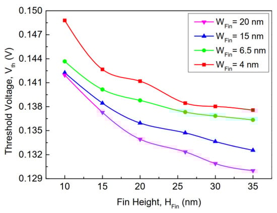
Figure 7.
Behavior of the threshold voltage as a function of fin height for FinFET devices with different values of the fin width at Vds = 0.05 V.
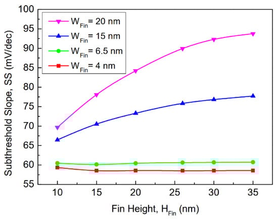
Figure 8.
Behavior of the subthreshold slope as a function of fin height for FinFET devices with different values of the fin width at Vds = 0.05 V.
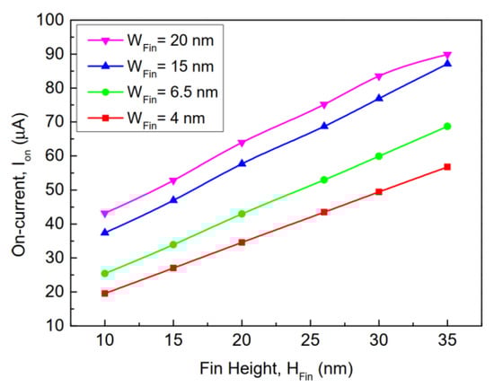
Figure 9.
Behavior of the on-current as a function of fin height for FinFET devices with different values of the fin width at Vgs = Vds = 0.8 V.
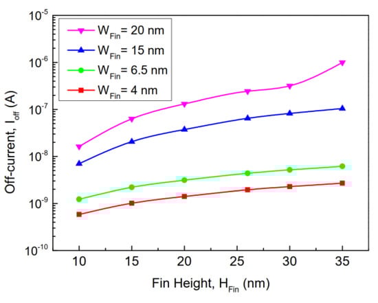
Figure 10.
Behavior of the leakage current as a function of fin height for FinFET devices with different values of the fin width at Vgs = 0 V and Vds = 0.8 V.
As is well-known, a higher Ion is well desired while the leakage current Ioff should be kept low in order to minimize the static power consumption. Figure 11 shows the effect of varying the fin height and the fin width on the Ion/Ioff ratio, which is a crucial figure of merit for digital applications. As shown in Figure 11, the Ion/Ioff ratio decreases with increasing Hfin and/or Wfin. It should be noticed that the highest value of the Ion/Ioff ratio occurs at the lowest height of 10 nm and then decreases approximately exponentially with increasing Hfin.
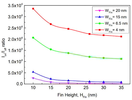
Figure 11.
Behavior of the current ratio Ion/Ioff as a function of fin height for FinFET devices with different values of the fin width at Vds = 0.8 V.
4.2. Impact of High-k Dielectric Materials on Device Performance
To analyze the effect of the gate dielectric materials on the device performance, the fin width, fin height, and gate length of the studied structure were fixed at 6.5, 26, and 20 nm, respectively. Figure 12 shows the total gate capacitance versus Vgs for different high-k dielectric materials. Under all of the studied cases, Cgg starts increasing as Vgs increases until saturation, and then it becomes roughly constant, as expected [4]. The value of Cgg increases with high-k dielectric material.
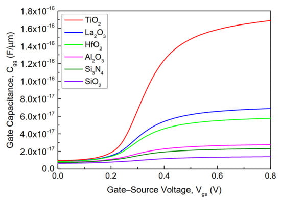
Figure 12.
Gate capacitance as a function of gate–source voltage with different gate dielectric materials at Vds = 0.05 V.
The change in transconductance and cut-off frequency with different gate dielectric materials is shown in Figure 13. The analyzed bias point is: Vgs = 0.2 V and Vds = 0.05 V. As can be observed from the figure, a remarkable improvement of the device performance is achieved using higher-k material [4,21]. The value of gm for TiO2 material is higher compared to the values obtained by using the other dielectric materials, implying a higher amplification capability of the device [4,22]. The resultant behavior of fT is mainly due to the impact of the high-k dielectric material on gm rather than on Cgg, as can be noticed from Figure 12 and Figure 13. The highest fT is obtained at Vgs = 0.2 V with Vds = 0.05 V for a FinFET model with TiO2 material, reflecting the better gate controllability over the channel fin region and hence higher transconductance.
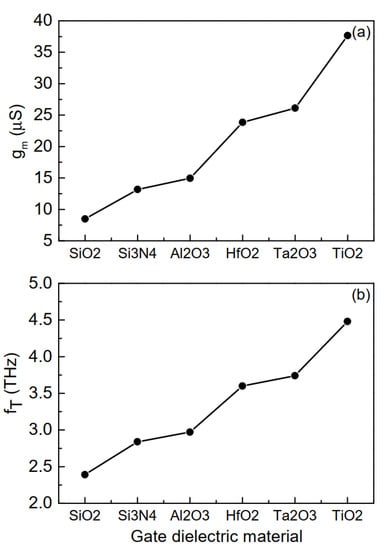
Figure 13.
Behavior of (a) transconductance and (b) cut-off frequency with different high-k gate dielectric materials at Vds = 0.05 V.
In short channel devices, the leakage current can be problematic for switching speed in the circuit by leading to an increase in the Ion/Ioff ratio. The use of a multigate design structure together with high-k dielectric materials proves good mitigation in device issues and demonstrates high switching speed in electric circuits [16,17,18,19,20,21,22]. Figure 14 shows the transfer I–V characteristics in a logarithmic scale of 14-nm SOI n-FinFET under on-state bias conditions (Vds = 0.8 V). It is observed that the off-state current decreases, especially with high-k. As expected, using high-k dielectric such as TiO2 is necessary for short channel devices to mitigate the leakage current. It is also observed that the current flow in the short channel can be improved by using high-k dielectric material. As reported in Figure 15, the highest value of Ion/Ioff occurs at the highest dielectric constant. For many electronic circuit applications, such as amplifiers and digital circuits, the best Ion/Ioff current ratio is at the highest value and therefore it implies better device performance.
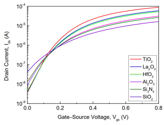
Figure 14.
Transfer I–V characteristics in logarithmic scale for FinFET devices with different gate dielectric materials at Vds = 0.8 V.
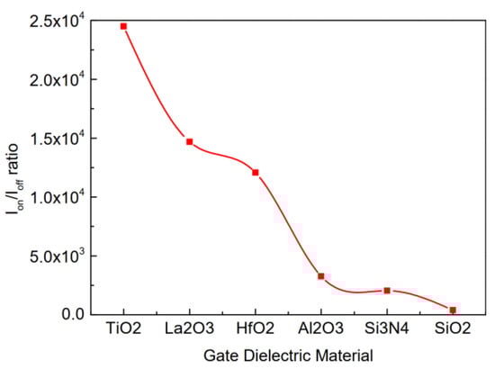
Figure 15.
Behavior of the current ratio Ion/Ioff as a function of gate dielectric materials for FinFET devices at Vds = 0.8 V.
4.3. Impact of the Gate Length on Device Performance
To analyze the effect of the gate length on the device performance, the fin width and fin height of the studied structure were fixed at 6.5 nm and 26 nm, respectively. Furthermore, the hafnium oxide was used as a gate dielectric material. There are full-node processes for FinFET technologies, such as 16, 14, 10, 7, 5, and 3 nm in R&D [1,2]. Thus, is very important to investigate the effect of the gate length on calibrated FinFET device performance. Varying device gate lengths can help in judging the numerical model’s accuracy in predicting the device characteristics. The change in transconductance with different gate lengths (from 5 nm to 20 nm) is shown in Figure 16. It can be observed from the figure that a remarkable limitation is achieved by scaling down the gate length. The gm for 10 nm gate length device reaches higher values compared to other devices with different gate lengths [4,18]. The fT behavior is mainly due to the gate length effect on gm rather than on Cgg, as can be noticed from Figure 16, Figure 17 and Figure 18. The highest fT is obtained at Vgs = 0.25 V with Vds = 0.05 V for a device with 5 nm gate length, as illustrated in Figure 18. To find the effect of the gate length on the device’s I–V characteristics, the gate length was varying from 5 nm to 20 nm. Figure 19 illustrates the effects of the gate length on transfer I–V curves of the device. It is well seen from the figure that reducing the gate length leads to a decrease in the threshold voltage, but it causes an increase in the leakage current (at Vgs = 0 V). The variation of the threshold voltage, subthreshold slope, and Ion/Ioff ratio at two gate lengths with different fin widths is shown in Figure 20, Figure 21 and Figure 22, respectively. As can be observed, Vth and SS are sensitive to Wfin for a small gate length due to the short channel effect as illustrated in Figure 20 and Figure 21, respectively [22,23,24,25,26,27]. As shown in Figure 22, the highest value of Ion/Ioff occurs at the lowest fin width.
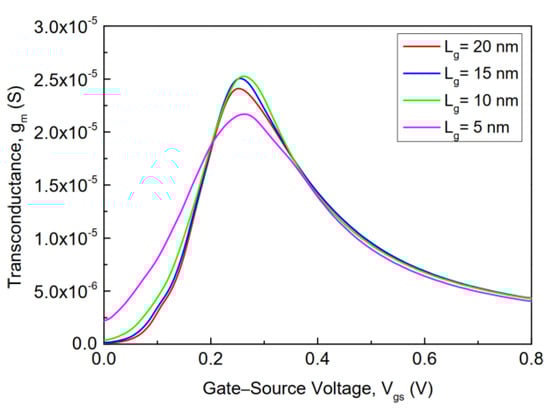
Figure 16.
Transconductance as a function of gate–source voltage with different gate lengths at Vds = 0.05 V.
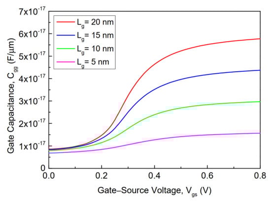
Figure 17.
Gate capacitance as a function of gate–source voltage with different gate lengths at Vds = 0.05 V.
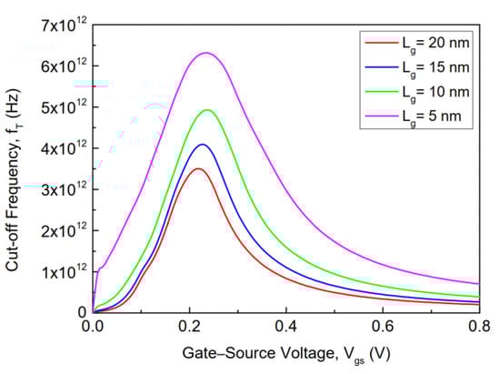
Figure 18.
Cut-off frequency as a function of gate–source voltage with different gate lengths at Vds = 0.05 V.
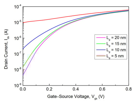
Figure 19.
Transfer characteristics logarithmic scale for FinFET devices with different gate lengths at Vds = 0.8 V.
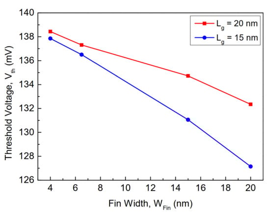
Figure 20.
Behavior of the threshold voltage as a function of fin width for FinFET devices with two different gate lengths at Vds = 0.05 V.
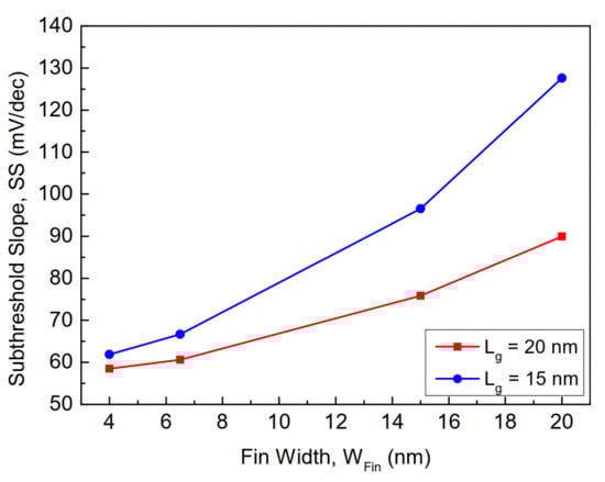
Figure 21.
Behavior of the subthreshold slope as a function of fin width for FinFET devices with two different gate lengths at Vds = 0.05 V.
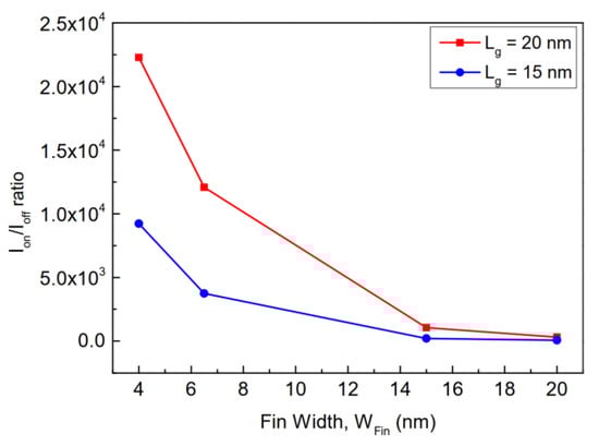
Figure 22.
Behavior of Ion/Ioff ratio as a function of fin width for FinFET devices with two different gate lengths at Vds = 0.8 V.
4.4. Device Optimization
Silicon material is used for the fabrication of an optimized FinFET device with a physical gate length of 15 nm. TiO2 is used as gate dielectric material to replace HfO2 for better controllability of the gate over the channel. As it is well-known, the electrostatic integrity can be improved by reducing the thickness of the gate oxide [26]. The high-k dielectric thickness is chosen to be 2 nm. Based on the previous investigation, the fin width and fin height are chosen to be equal to 4 nm and 35 nm, respectively. Fin width was scaled down in order to improve FinFET electrostatics. The source/drain spacers are fixed to 7 nm and covered by Si3N4. The contact resistivity at the S/D contact/silicon interface is fixed to 10−9 Ω.cm2. The proposed device with the above characteristics shows a good improvement in electrical parameters such as Ion, SS, and DIBL compared to calibrated FinFET [1]. This proves that the improvement of SCEs in the FinFET device reduces sensitivity to the leakage current. It is also interesting to note that Ion/Ioff ratio is approximatively two times greater than the calibrated FinFET. Better device switching (on/off) can result from steeping SS and a larger Ion/Ioff ratio. Table 3 illustrates a comparison of the optimized and calibrated device parameters with different 14-nm FinFET device technologies [28,29,30].
Table 3.
Comparison of different 14-nm SOI n-FinFET device technologies.
Finally, it should be highlighted that nowadays the interest for the FinFET technology is spreading more and more in many fields of application—such as single-molecule detection [31], pH sensing [32,33], biomedicine [34], label-free biosensing [35], 5G power amplifiers [36], energy harvesting [37], and space application [38], just to mention a few. This wide and ever-expanding range of applications makes evident the increasing need for an accurate optimization of the FinFET structure to satisfy the specific constraints and requirements.
5. Conclusions
In this study, the 3D 14-nm SOI n-FinFET was successfully simulated, performed, and calibrated to experimental data by using Silvaco tools. The effects of varying the fin width, fin height, gate dielectric material, and gate length on device performance were analyzed in terms of both DC and RF parameters. The results indicated that low leakage current and high Ion/Ioff ratio can be obtained with small Wfin and Hfin. A cut-off frequency on the order of 1 THz was simulated and reported for the investigated FinFET model. The results indicated that this frequency is increased for smaller fin width and a subsequent reduction of gate transconductance. For the optimized device, a transconductance of 69.33 µS and a cut-off frequency of 4.22 THz were achieved at Vds = 0.05 V with Vgs = 0.23 V and Vgs = 0.22 V, respectively, by using the TiO2 as the gate dielectric at 15-nm gate length. The developed study provided some useful insights outlining the great potential of the FinFET technology nodes for RF applications with high performance and low power consumption.
Author Contributions
Conceptualization, N.E.I.B.; Methodology, N.E.I.B.; Software, N.E.I.B.; Validation, N.E.I.B., T.R.L. and S.P.; Investigation, N.E.I.B.; Writing—original draft preparation, N.E.I.B.; Writing—review and editing, S.P. and G.C.; Supervision, S.P. and G.C. All authors have read and agreed to the published version of the manuscript.
Funding
This research received no external funding.
Acknowledgments
This work was partially supported by Semiconductor Laboratory (GE01/08), Kuwait University.
Conflicts of Interest
The authors declare no conflict of interest. The funders had no role in the design of the study; in the collection, analyses, or interpretation of data; in the writing of the manuscript, or in the decision to publish the results.
References
- Lin, C.H.; Greene, B.; Narasimha, S.; Cai, J.; Bryant, A.; Radens, C.; Narayanan, V.; Linder, B.; Ho, H.; Aiyar, A.; et al. High performance 14nm SOI FinFET CMOS technology with 0.0174 µm 2 embedded DRAM and 15 levels of Cu metallization. In Proceedings of the 2014 IEEE International Electron Devices Meeting, San Francisco, CA, USA, 15–17 December 2014; pp. 3–8. [Google Scholar]
- Sun, J.; Li, X.; Sun, Y.; Shi, Y. Impact of geometry, doping, temperature, and boundary conductivity on thermal characteristics of 14-nm bulk and SOI FinFETs. IEEE Trans. Device Mater. Reliab. 2020, 20, 119–127. [Google Scholar] [CrossRef]
- Kumar, U.S.; Rao, V.R. A thermal-aware device design considerations for nanoscale SOI and bulk FinFETs. IEEE Trans. Electron Devices 2015, 63, 280–287. [Google Scholar] [CrossRef]
- Jena, K.; Swain, R.; Lenka, T.R. Effect of thin gate dielectrics on DC, radio frequency and linearity characteristics of lattice-matched AlInN/AlN/GaN metal–oxide–semiconductor high electron mobility transistor. IET Circuits Devices Syst. 2016, 10, 423–432. [Google Scholar] [CrossRef]
- Mishra, S.; Parihar, N.; Anandkrishnan, R.; Dabhi, C.K.; Chauhan, Y.S.; Mahapatra, S. NBTI-related variability impact on 14-nm node FinFET SRAM performance and static power: Correlation to time zero fluctuations. IEEE Trans. Electron Devices 2018, 65, 4846–4853. [Google Scholar] [CrossRef]
- Boukortt, N.; Patanè, S.; Crupi, G. 3D investigation of 8-nm tapered n-FinFET model. Silicon 2020, 12, 1585–1591. [Google Scholar] [CrossRef]
- Boukortt, N.; Hadri, B.; Patanè, S.; Caddemi, A.; Crupi, G. Investigation on TG n-FinFET parameters by varying channel doping concentration and gate length. Silicon 2017, 9, 885–893. [Google Scholar] [CrossRef]
- Yoon, J.-S.; Baek, R.-H. Device Design Guideline of 5-nm-Node FinFETs and Nanosheet FETs for Analog/RF Applications. IEEE Access. 2020, 8, 189395–189403. [Google Scholar] [CrossRef]
- Boukortt, N.; Hadri, B.; Patanè, S.; Caddemi, A.; Crupi, G. Electrical Characteristics of 8-nm SOI n-FinFETs. Silicon 2016, 8, 497–503. [Google Scholar] [CrossRef]
- Boukortt, N.E.I.; Hadri, B.; Caddemi, A.; Crupi, G.; Patane, S. 3-D Simulation of Nanoscale SOI n-FinFET at a Gate Length of 8 nm Using ATLAS SILVACO. Trans. Electr. Electron. Mater. 2015, 16, 156–161. [Google Scholar] [CrossRef]
- Boukortt, N.E.I.; Hadri, B.; Caddemi, A.; Crupi, G.; Patane, S. Temperature Dependence of Electrical Parameters of Silicon-on-Insulator Triple Gate n-Channel Fin Field Effect Transistor. Trans. Electr. Electron. Mater. 2016, 17, 329–334. [Google Scholar] [CrossRef]
- Natarajan, S.; Agostinelli, M.; Akbar, S.; Bost, M.; Bowonder, A.; Chikarmane, V.; Chouksey, S.; Dasgupta, A.; Fischer, K.; Fu, Q.; et al. A 14 nm logic technology featuring 2 nd-generation finfet, air-gapped interconnects, self-aligned double patterning and a 0.0588 µm 2 sram cell size. In Proceedings of the 2014 IEEE International Electron Devices Meeting, San Francisco, CA, USA, 15–17 December 2014; pp. 3–7. [Google Scholar]
- User Guide Manual, ATLAS, Version 5.28.1.R USA; Silvaco Inc.: San Francisco, CA, USA, 2019.
- Subramanian, V.; Parvais, B.; Borremans, J.; Mercha, A.; Linten, D.; Wambacq, P.; Loo, J.; Dehan, M.; Gustin, C.; Collaert, N.; et al. Planar Bulk MOSFETs Versus FinFETs: An Analog/RF Perspective. IEEE Trans. Electron. Devices 2006, 53, 3071–3079. [Google Scholar] [CrossRef]
- Martinez-Lopez, A.G.; Cerdeira, A.; Tinoco, J.C.; Alvarado, J.; Padron, W.Y.; Mendoza, C.; Raskin, J.-P. RF modeling of 40-nm SOI triple-gate FinFET. Int. J. Numer. Model. 2015, 28, 465–478. [Google Scholar] [CrossRef]
- Crupi, G.; Schreurs, D.M.P.; Caddemi, A. Effects of gate-length scaling on microwave MOSFET performance. Electronics 2017, 6, 62. [Google Scholar] [CrossRef]
- Sreenivasulu, V.B.; Narendar, V. A comprehensive analysis of junctionless tri-gate (TG) FinFET towards low-power and high-frequency applications at 5-nm gate length. Silicon 2021, 1–13. [Google Scholar] [CrossRef]
- Huang, S.E.; Yu, C.L.; Su, P. Investigation of fin-width sensitivity of threshold voltage for InGaAs and Si negative-capacitance FinFETs considering quantum-confinement effect. IEEE Trans. Electron Devices 2019, 66, 2538–2543. [Google Scholar] [CrossRef]
- Colinge, J.P. Multiple-gate soi mosfets. Solid-State Electron. 2004, 48, 897–905. [Google Scholar] [CrossRef]
- Kurniawan, E.D.; Yang, H.; Lin, C.C.; Wu, Y.C. Effect of fin shape of tapered FinFETs on the device performance in 5-nm node CMOS technology. Microelectron. Reliab. 2018, 83, 254–259. [Google Scholar] [CrossRef]
- Thorp, J.S.; Evans, D.; Al-Naief, M.; Akhtaruzzaman, M. The dielectric properties of aluminium nitride substrates for microelectronics packaging. J. Mater. Sci. 1990, 25, 4965–4971. [Google Scholar] [CrossRef]
- Gorchichko, M.; Cao, Y.; Zhang, E.X.; Yan, D.; Gong, H.; Zhao, S.E.; Wang, P.; Jiang, R.; Liang, C.; Fleetwood, D.M.; et al. Total-ionizing-dose effects and low-frequency noise in 30-nm gate-length bulk and SOI FinFETs with SiO2/HfO2 gate dielectrics. IEEE Trans. Nucl. Sci. 2019, 67, 245–252. [Google Scholar] [CrossRef]
- Crupi, G.; Caddemi, A.; Schreurs, D.M.M.-P.; Wiatr, W.; Mercha, A. Microwave noise modeling of FinFETs. Solid-State Electron. 2011, 56, 18–22. [Google Scholar] [CrossRef]
- Crupi, G.; Schreurs, D.M.M.-P.; Caddemi, A.; Angelov, I.; Homayouni, M.; Raffo, A.; Vannini, G.; Parvais, B. Purely analytical extraction of an improved nonlinear FinFET model including non-quasi-static effects. Microelectron. Eng. 2009, 86, 2283–2289. [Google Scholar] [CrossRef]
- Jin, X.; Ou, J.J.; Chen, C.H.; Liu, W.; Deen, M.J.; Gray, P.R.; Hu, C. An effective gate resistance model for CMOS RF and noise modeling. In Proceedings of the International Electron Devices Meeting 1998. Technical Digest (Cat. No.98CH36217), San Francisco, CA, USA, 6–9 December 1998; pp. 961–964. [Google Scholar]
- Park, J.; Kim, J.; Showdhury, S.; Shin, C.; Rhee, H.; Yeo, M.S.; Cho, E.C.; Yi, J. Electrical Characteristics of Bulk FinFET According to Spacer Length. Electronics 2020, 9, 1283. [Google Scholar] [CrossRef]
- Lee, K.L.; He, R.Y.; Huang, H.W.; Yeh, C.C.; Li, I.H.; Cheng, O. A study of fin width effect on the performance of FinFET. In Proceedings of the 2015 IEEE 22nd International Symposium on the Physical and Failure Analysis of Integrated Circuits, Hsinchu, Taiwan, 29 June–2 July 2015; pp. 503–504. [Google Scholar]
- Zhang, J.; Niu, G.; Cai, W.; Imura, K. Comparison of PMOS and NMOS in a 14-nm RF FinFET technology: RF Characteristics and Compact Modeling. In Proceedings of the 2020 IEEE 20th Topical Meeting on Silicon Monolithic Integrated Circuits in RF Systems (SiRF), San Antonio, TX, USA, 26–29 January 2020; pp. 47–49. [Google Scholar]
- Wang, G.; Qin, C.; Yin, H.; Luo, J.; Duan, N.; Yang, P.; Gao, X.; Yang, T.; Li, J.; Yan, J.; et al. Study of SiGe selective epitaxial process integration with high-k and metal gate for 16/14nm nodes FinFET technology. Microelectron. Eng. 2016, 163, 49–54. [Google Scholar] [CrossRef]
- Mah, S.K.; Ker, P.J.; Ahmad, I.; Zainul Abidin, N.F.; Ali Gamel, M.M. A Feasible Alternative to FDSOI and FinFET: Optimization of W/La2O3/Si Planar PMOS with 14 nm Gate-Length. Materials 2021, 14, 5721. [Google Scholar] [CrossRef]
- Santermans, S.; Barge, D.; Hellings, G.; Mori, C.B.; Migacz, K.J.; Rip, J.; Spampinato, V.; Vos, R.; Du Bois, B.; Chaudhuri, A.R.; et al. 50 nm Gate Length FinFET Biosensor & the Outlook for Single-Molecule Detection. In Proceedings of the 2020 IEEE International Electron Devices Meeting (IEEE-IEDM), San Francisco, CA, USA, 12–18 December 2020; pp. 35.4.1–35.4.4. [Google Scholar]
- Rani, D.; Rollo, S.; Olthuis, W.; Krishnamoorthy, S.; Pascual García, C. Combining Chemical Functionalization and FinFET Geometry for Field Effect Sensors as Accessible Technology to Optimize pH Sensing. Chemosensors 2021, 9, 20. [Google Scholar] [CrossRef]
- Medina-Bailon, C.; Kumar, N.; Dhar, R.P.S.; Todorova, I.; Lenoble, D.; Georgiev, V.P.; García, C.P. Comprehensive Analytical Modelling of an Absolute pH Sensor. Sensors 2021, 21, 5190. [Google Scholar] [CrossRef]
- Coluccio, M.L.; Pullano, S.A.; Vismara, M.F.M.; Coppedè, N.; Perozziello, G.; Candeloro, P.; Gentile, F.; Malara, N. Emerging Designs of Electronic Devices in Biomedicine. Micromachines 2020, 11, 123. [Google Scholar] [CrossRef] [PubMed]
- Dixit, A.; Samajdar, D.P.; Chauhan, V. Sensitivity Analysis of a Novel Negative Capacitance FinFET for Label-Free Biosensing. IEEE Trans. Electron Devices 2021, 68, 5204–5210. [Google Scholar] [CrossRef]
- Daneshgar, S.; Dasgupta, K.; Thakkar, C.; Chakrabarti, A.; Levy, C.S.; Jaussi, J.E.; Casper, B. High-Power Generation for mm-Wave 5G Power Amplifiers in Deep Submicrometer Planar and FinFET Bulk CMOS. IEEE Trans. Microw. Theory Tech. 2020, 68, 2041–2056. [Google Scholar] [CrossRef]
- Whittaker, K.; Rizkalla, M.; Ytterdal, T. A Low Power FinFET Charge Pump for Energy Harvesting Applications. In Proceedings of the 2020 IEEE 63rd International Midwest Symposium on Circuits and Systems (MWSCAS), Springfield, MA, USA, 9–12 August 2020; pp. 1048–1051. [Google Scholar] [CrossRef]
- Cai, C.; Gao, S.; Zhao, P.; Yu, J.; Zhao, K.; Xu, L.; Li, D.; He, Z.; Yang, G.; Liu, T.; et al. SEE Sensitivity Evaluation for Commercial 16 nm SRAM-FPGA. Electronics 2019, 8, 1531. [Google Scholar] [CrossRef]


Publisher’s Note: MDPI stays neutral with regard to jurisdictional claims in published maps and institutional affiliations. |
© 2021 by the authors. Licensee MDPI, Basel, Switzerland. This article is an open access article distributed under the terms and conditions of the Creative Commons Attribution (CC BY) license (https://creativecommons.org/licenses/by/4.0/).