Article

Gain Expressions for Capacitive Wireless Power Transfer with One Electric Field Repeater

1
Department of Industrial Science and Technology, Odisee University College of Applied Sciences, 9000 Ghent, Belgium
2
Department of Engineering for Innovation, University of Salento, 73100 Lecce, Italy
3
Department of Electrical, Electronic and Information Engineering Guglielmo Marconi, University of Bologna, 40126 Bologna, Italy
4
Department of Engineering, University of Perugia, 06123 Perugia, Italy
*
Author to whom correspondence should be addressed.
Electronics 2021, 10(6), 723; https://doi.org/10.3390/electronics10060723
Submission received: 15 February 2021 / Revised: 14 March 2021 / Accepted: 16 March 2021 / Published: 18 March 2021

Abstract

:
In this paper, the use of a repeater element between the transmitter and the receiver of a capacitive wireless power transfer system for achieving larger transfer distances is analyzed. A network formalism is adopted and the performance described by using the three power gains usually adopted in the context of two-port active networks. The analytical expressions of the gains as function of the network elements are derived. Assuming that the parameters of the link are given and fixed, including the coupling factors between transmitter, repeater and receiver, the conditions for maximizing the different gains by acting on the network terminating impedances (i.e., load and internal source conductance) are determined. The analytical formulas are verified through circuital simulations.

1. Introduction

Wireless power transfer (WPT) allows the charging of electrical devices without the need to plug in a physical cable. This has several advantages, among others [1,2,3,4]:
  • The main advantage, especially for portable equipment, is the practicality and user experience. Wireless energy transfer eliminates the hassle of connecting cables to charge the device. This applies to consumers as well as in an industrial setting.
  • Wirelessly charged devices lead to higher durability and robustness because no open connections are required. There is no more wear and tear on the charging connector; the appliance is completely lockable, making it water and dust proof. This is often a requirement in industrial environments. Indeed, during wired charging, sparks can occur when connecting or disconnecting the charging cable from the device. Wireless charging increases safety in hazardous industrial environments where flammable or combustible atmospheres are present.
  • Wireless charging facilitates device miniaturization by omitting a large charger connector or reducing the size of the battery. In addition, for certain applications, it is expensive, dangerous or unfeasible to replace the batteries of the device or to connect charging cables (e.g., charging Internet of Things sensor networks or medical implants).
  • Smart devices are able to detect their low battery voltage and can automatically report to a charging station for recharging (automated guided vehicles, robots, drones, ) Wireless charging of these smart devices without any human intervention leads to more automated, reliable and energy-efficient operation.
Different methods exist to realize WPT, for example, microwave [5,6] and optical WPT [7] allow for power transfer of several kilometers. In this work, focus will lie on capacitive wireless power transfer (CPT) which utilizes the electric field as medium to transfer energy from a transmitter to a receiver. Applications include the charging of electric vehicles [8], automatic guided vehicles [9], biomedical implants [10], integrated circuits [11] and low-power consumer applications [12].
Compared to inductive wireless power transfer (IPT), which exploits the magnetic field, it has several advantages such as the absence of eddy-current losses, lower heat dissipation, a larger tolerance to misalignment and a lower system cost and weight [13,14]. However, an important limitation of CPT compared to IPT are the unfavourable attributes that arise for long distance applications in the tens of range and more, in particular for higher power applications. These drawbacks include large transmitter/receiver plates, high operating voltages, high switching frequencies and high electric fields which can cause safety concerns [15]. The main cause is the lower power density compared to IPT for long range applications because of the low coupling capacitance, usually in the picofarad (pF) range [13].
By applying an electric field repeater, the power transfer distance can be increased without the aforementioned drawbacks [13,16]. It is located between the transmitter and receiver, to further extend the electric field towards the receiver (Figure 1). It is not galvanically connected to transmitter or receiver. The repeater is comparable to the concept of relay resonators for IPT to increase the transfer distance [17,18,19,20,21].
Figure 1 depicts a schematic overview: energy is transferred wirelessly from a transmitter source I S to a load Y l o a d via an intermediate repeater. Compensation circuits are present in transmitter, repeater and receiver to create resonance at an operating angular frequency ω 0 .
Standard gain expressions are often employed to describe an energy system behavior, in particular in the context of two-port active networks such as amplifiers [22]. Three gain definitions are most commonly used:
  • The power gain G P is defined as the ratio between the active power P L delivered to the load and the active input power P i n to the system.
  • The available gain G A equals the ratio between the maximum available active load power P A and the available active input power P A G .
  • The transducer gain G T is given by the ratio between the power P L delivered to the load and the available input power P A G .
The use of these three power gains as figures of merit for describing the performance of a WPT link has already been suggested in previous works in which the gain expressions for the IPT case have been derived and discussed [21,23]. In fact, the use of the three power gains instead of various efficiency definitions has the following advantages:
  • Different definitions of the efficiency are sometimes used in context of WPT. The use of the power gains eliminates possible ambiguity to the efficiency definition. In fact, the three gain definitions are well established and their expressions in terms of the possible matrix descriptions of the network (e.g., impedance, admittance, scattering matrix) are available.
  • The gain expressions are often available in common microwave circuital simulators thus simplifying calculations and optimizations of the network parameters.
It is worth observing that depending on the specific application of interest, the three gains can all be equally useful. In fact, although, all WPT links have a common general goal which is to transfer power from a generator to a load, each application imposes specific requirements which can be translated into maximizing one gain rather than another. Consider the following examples.
  • Transducer Gain Maximization. For certain applications, the goal is to maximize the amount of power available from the source that is delivered to the load. Consider for instance high power applications (e.g., the charging of electric vehicles), for which it is important not to waste power in each section of the circuit, i.e., power reflections at both the input and the output ports have to be minimized. This goal can be achieved by maximizing the transducer gain.
  • Power/Available Gain Maximization. In other applications, the focus is on one of the two ports and the goal is to minimize power reflections at either the output or the input port. For example, in the case where the load is a medical implant, attention is focused on the output port of the WPT link: it is essential to be able to transfer to the load all the power available at the output port of the link while any reflections at the input port play a less important role and can be compensated for by increasing the power available from the generator. A such goal can be obtained by maximizing the power gain. While the gain to be maximized is the available gain when the goal is to minimize power reflections at the input port.
According to the aforementioned advantages of using the three power gains for describing the performance of the CPT system, in this work their expressions as function of the network elements are derived for the first time in the literature. Moreover, the terminating load and internal source conductance that maximize the gains are analytically determined for the resonant CPT system with one electric field repeater. More specifically, the contributions of this work are as follows:
  • First, the different gain expressions are described for a general two-port system, characterized by its admittance matrix (Section 2).
  • Next, it is discussed how, for a given two-port network, the different gains can be maximized by optimizing the load and/or source conductance (Section 3).
  • These results are applied to the CPT system with one repeater in Section 4: an equivalent circuit is proposed for which the different gain expressions are derived.
  • In the same section, the conditions for maximizing the different gains (i.e., the optimal terminating load and/or internal source conductance) are determined. Furthermore, the expressions for the maximum attainable gain is solved for the CPT system with one repeater.
  • Finally, the analytical derivation is verified by numerical circuit simulation for an example CPT system with one repeater (Section 5).
The main novelty of this work is that, for the first time, a detailed analysis of a CPT system with one repeater is performed, focused on the power gains which describe the overall performance of the system.

2. Gain Definitions

2.1. A General Loaded Two-Port Network

In this section, the different gain definitions will be recalled. An admittance representation will be chosen, since it simplifies the results for a CPT system and is still fully equivalent to the more common impedance representation. In this and the following section, a general (reciprocal or non-reciprocal) circuit is considered. The CPT configuration with one repeater is only studied from Section 4.
Consider a two-port network (Figure 2a), fully characterized by its admittance matrix Y with elements y i j = g i j + j b i j ( i , j = 1 , 2 ). The input of the network is connected to a generator, represented by a current source I S with internal admittance Y S . The output is connected to a load admittance Y L = G L + j B L , with G L the load conductance and B L the load susceptance. At the ports, peak voltage phasors V i and peak current phasors I i are present ( i = 1 , 2 ), as defined in the figure, and related by:
I 1 I 2 = y 11 y 12 y 21 y 22 · V 1 V 2 .
The input admittance of the network is called Y i n = G i n + j B i n , with G i n the input conductance and B i n the input susceptance. From I 2 = Y L · V 2 and (1), it follows that:
Y i n = I 1 V 1 = y 11 y 12 y 21 y 22 + Y L .
To determine the gain functions, it is useful to derive the Norton equivalent circuit of the two-port loaded with Y L (Figure 2b) [24]. The output admittance when I S is open-circuited is given by Y o u t = G o u t + j B o u t and can be derived from I 1 = Y S · V 1 and (1):
Y o u t = I 2 V 2 | I S = 0 = y 22 y 12 y 21 y 11 + Y S .
From Kirchhoff’s current law and (1), the Norton current I n o can be determined:
I n o = I 2 | V 2 = 0 = y 21 y 11 + Y S I S .
The power gain definitions are expressed as a ratio of output power to input power. However, different ways exist to define input and output power. Depending on which power definitions are used, different gains are obtained. The three commonly used gains are explained in the following parts of this section.

2.2. Power Gain

The power gain G P is defined as
G P = P L P i n .
P L is the power dissipated in the load conductance G L (Figure 2a):
P L = 1 2 G L | V 2 | 2 .
P i n is the active power entering the two-port network (Figure 2a):
P i n = 1 2 G i n | V 1 | 2 .
Since both P L and P i n are independent on the generator’s internal admittance Y S , the power gain G P is also independent on Y S .
By combining (6) and (7), it is found that:
G P = G L G i n | V 2 V 1 | 2 = G L G i n | y 21 y 22 + Y L | 2 .
Note that G P of a two-port system can only be defined if a value for the load Y L is specified.
In the context of WPT systems, G P coincides with the definition that is sometimes used for the efficiency.

2.3. Available Gain

The available gain G A is defined as
G A = P A P A G .
P A is the maximum available load power, i.e., the maximum power that can be dissipated into a load. This occurs at a specific value of the load, i.e., if the load value is chosen so that the the complex conjugate matching is realized at the output port of the link: Y L = Y o u t * , with * indicating the complex conjugate (see Figure 2b). Accordingly, P A is given by:
P A = | I n o | 2 8 G o u t .
P A G is the input power available from the generator, i.e., the maximum power that can be put into the two-port network by a generator. This is achieved when the complex conjugate matching is realized at the input port, i.e., for Y i n = Y S * (Figure 2c). Accordingly, P A G is given by:
P A G = | I S | 2 8 G S .
Since both P A and P A G are independent on the load admittance Y L , the available gain G A is also independent on Y L .
The ratio of (10) and (11) results as:
G A = G S G o u t | I n o I S | 2 = G S G o u t | y 21 y 11 + Y S | 2 .
Note that G A of a two-port system can only be defined if a value for Y S is specified.

2.4. Transducer Gain

The transducer gain G T is defined as
G T = P L P A G ,
and is dependent on both the internal admittance Y S and the load admittance Y L . Both have to be specified in order to be able to define G T .
With (6) and (11), it follows that
G T = 4 G L G S | V 2 I S | .
From Kirchhoff’s current law, it is obtained that I S = V 1 ( Y i n + Y S ) . Combining with (1) and I 2 = Y L · V 2 , the transducer gain G T can finally be expressed as:
G T = 4 G L G S | y 21 ( y 11 + Y S ) ( y 22 + Y L ) y 12 y 21 | 2 .
Maximizing G T corresponds to maximizing the amount of power delivered to the load for a fixed available input power of the generator. In order to maximize G T the complex conjugate matching has to be realized at both the input and the output port: Y i n = Y S * and Y o u t = Y L * .
Table 1 shows an overview of the general expressions of the different gains.

3. Maximizing the Gains

In this section, it will be discussed how each gain can be maximized by changing Y S and/or Y L . The two-port network Y is considered fixed. In the previous section, it was discussed that:
  • The available gain G A is independent of Y L while it depends on Y S . The value of the source admittance Y S that maximizes G A is called Y c 1 .
  • The power gain G P is independent of Y S while it depends on Y L . The value of the load Y S that maximizes G P is called Y c 2 .
The values of Y c 1 and Y c 2 will now be determined. From the gain definitions, it follows that
G P = G T if Y S = Y i n *
G A = G T if Y L = Y o u t *
Moreover,
G T G P
G T G A
since
P L P A
P i n P A G .
Combining the above statements, it follows that G T achieves its maximum value if
Y S = Y c 1 = Y i n *
and
Y L = Y c 2 = Y o u t * .
Notice that under these conditions, G P = G A = G T = G M , with G M the ultimate gain. In other words, if the source and load admittances meet (22) and (23), the three gains are maximized and equal each other. These conditions are visually represented in Figure 3.
Solving the system of Equations (22) and (23), taken into account (2) and (3), the admittances Y c 1 and Y c 2 are found:
Y c 1 = G c 1 + j B c 1 = g 11 ( θ g + j θ b ) j b 11
Y c 2 = G c 2 + j B c 2 = g 22 ( θ g + j θ b ) j b 22
with the following definitions:
θ g = 1 g c 2 g 11 g 22 1 + b c 2 g 11 g 22
θ b = g c b c g 11 g 22
g c + j b c = y 12 y 21 .
The admittances Y c 1 and Y c 2 are called the conjugate image admittances, analogous to [25].

4. Capacitive Wireless Power System with One Repeater

4.1. Equivalent Circuit

Figure 4 depicts the equivalent circuit of the CPT system with one electric field repeater as given in Figure 1. The subscripts 1, 2 and 3 are used for the transmitter, receiver and repeater, respectively.
The supply of the transmitter is represented by the current source I S with angular frequency ω 0 . It is assumed that the internal admittance Y S of the source is purely real ( Y S = G S ), as well as the load ( Y L = G L ). The losses in the circuit are represented by the conductances G i ( i = 1 , 2 , 3 ). The electric coupling between the transmitter and the repeater is represented by coupled capacitances C 1 and C 3 with mutual capacitance C 13 . The corresponding coupling factor k 13 is defined as:
k 13 = C 13 C 1 C 3 .
Note that this does not represent the physical structure of the coupled CPT plates, but an equivalent representation thereof [26,27]. Analogously, the electric coupling between the receiver and the field repeater is symbolized by C 2 , C 3 and mutual capacitance C 23 . The corresponding coupling factor k 23 is given by:
k 23 = C 23 C 2 C 3 .
It is assumed that there is no electric coupling between the transmitter and the receiver, i.e., the coupling factor k 13 = 0 . In practical applications, the distance between transmitter and receiver is sufficiently large to neglect this coupling.
Resonance at transmitter, repeater and receiver is realized by adding a shunt inductor L i ( i = 1 , 2 , 3 ) with value
L i = 1 ω 0 2 C i .
In the rest of this work, it is assumed that the parameters of the wireless link are given and fixed, including the coupling factors between transmitter, repeater and receiver.

4.2. Admittance Matrix

From Kirchhoff’s current law, the relation between the currents and voltages at angular resonance frequency ω 0 is obtained:
I 1 = G 1 V 1 + j ω 0 C 13 V 3
I 2 = G 2 V 2 + j ω 0 C 23 V 3
0 = G 3 V 3 + j ω 0 C 13 V 1 + j ω 0 C 23 V 2 .
The equivalent circuit of Figure 4 can be modelled as a two-port network with admittance matrix Y . From (1), (32)–(34), the admittance matrix Y can be determined:
Y = 1 G 3 G 1 G 3 + ω 0 2 C 13 2 ω 0 2 C 13 C 23 ω 0 2 C 13 C 23 G 2 G 3 + ω 0 2 C 23 2 .
Note that all matrix elements are real.
The symbols in Table 2 are defined. The unloaded quality factors Q i of each resonator are introduced. The external quality factors of the transmitter and receiver are called Q S and Q L , respectively, while the corresponding loaded quality factors are Q 1 T and Q 2 T . The susceptance B 0 of the capacitance at the receiver is applied as normalization factor. The transformation ratios are given by n i j . Finally, the parameters χ i j , χ 1 T 3 and χ 32 T are introduced in order to alleviate the notation.
With these definitions, the admittance matrix elements are expressed by:
y 11 = g 11 = B 0 n 12 2 Q 1 ( 1 + χ 13 2 )
y 12 = y 21 = g 12 = B 0 n 12 Q 1 Q 2 χ 13 χ 23
y 22 = g 22 = B 0 Q 2 ( 1 + χ 23 2 ) .

4.3. Input and Output Admittance

Combining the admittance matrix elements (36)–(38) with (2) and (3) results in the input and output conductance of the set-up:
G i n = B 0 n 12 2 Q 1 · 1 + χ 13 2 + χ 32 T 2 1 + χ 32 T 2
G o u t = B 0 Q 2 · 1 + χ 23 2 + χ 1 T 3 2 1 + χ 1 T 3 2 .

4.4. Conjugate Image Admittances

Since the admittance matrix Y of the CPT-system is real, the conjugate image admittances are also real and can be referred to as conjugate image conductances. Combining the admittance matrix elements (36)–(38) with (24) and (25) results into:
Y c 1 = G c 1 = B 0 n 12 2 Q 1 · ( 1 + χ 13 2 ) ( 1 + χ 13 2 + χ 23 2 ) 1 + χ 23 2
Y c 2 = G c 2 = B 0 Q 2 · ( 1 + χ 23 2 ) ( 1 + χ 13 2 + χ 23 2 ) 1 + χ 13 2 .

4.5. Gains

Finally, the gains for the CPT-system with one repeater can be derived by combining the admittance matrix elements (36)–(38) with the general expressions for the gains. An overview can be found in Table 3.
From (8), the power gain G P is derived:
G P = χ 13 2 χ 32 T 2 ( 1 + χ 32 T 2 ) ( 1 + χ 13 2 + χ 32 T 2 ) · Q 2 T Q L .
Note that G P is dependent on the two-port network elements and the load, but not on the source admittance.
The expression for the available gain G A follows from (12):
G A = Q 1 T Q S · χ 1 T 3 2 χ 23 2 ( 1 + χ 1 T 3 2 ) ( 1 + χ 23 2 + χ 1 T 3 2 ) ,
and is independent on the load.
By applying (15), the transducer gain G T is found:
G T = Q 1 T Q S · 4 χ 1 T 3 2 χ 32 T 2 ( 1 + χ 1 T 3 2 + χ 32 T 2 ) 2 · Q 2 T Q L .
If Y S = Y c 1 and Y L = Y c 2 , the gains are maximized and equal the ultimate gain G M . Inserting (41) and (42) into the gain expressions results into:
G M = 1 + χ 13 2 + χ 23 2 ( 1 + χ 13 2 ) ( 1 + χ 23 2 ) 2 χ 13 2 χ 23 2 .

5. Numerical Verification

The previous analytical derivation is validated by a numerical example that has been analyzed by using the AWR Design Environment circuit simulator.
In more detail, a CPT system with one repeater is considered. The analyzed parameters are summarized in Table 4. The operating frequency is f 0 equal to 10 M Hz . The shunt lumped inductors L i have to be set so to make the capacitors C i resonating at f 0 .
From (29), (30), (31), (41), (42) and (46), the coupling factors, shunt inductances, conjugate image conductances and ultimate gain are calculated (Table 5).
Circuital simulations have been performed by analyzing the equivalent circuit illustrated in Figure 4 with the values of the parameters summarized in Table 4 and Table 5. First of all simulations have been performed by varying the load resistance R L = 1 / G L and the source internal resistance R S = 1 / G S . The results obtained for the three power gains are illustrated in Figure 5 and Figure 6. It is worth mentioning that the three power gains are figures of merit directly available in the simulation environment. As it can be seen, circuital simulations confirm the values calculated from theoretical formulas for the optimal values of R L and R S , i.e., R L = 171.21 Ω and R S = 77.34 Ω . Furthermore, the value of G M = 56.05% is confirmed. This is an increase compared to a default source and load impedance of 50 Ω for which the following values are obtained: G P = 43.31%, G A = 54.25% and G T = 42.88%. By inserting an impedance matching circuit, the source and load impedances can be adapted to the optimal values.
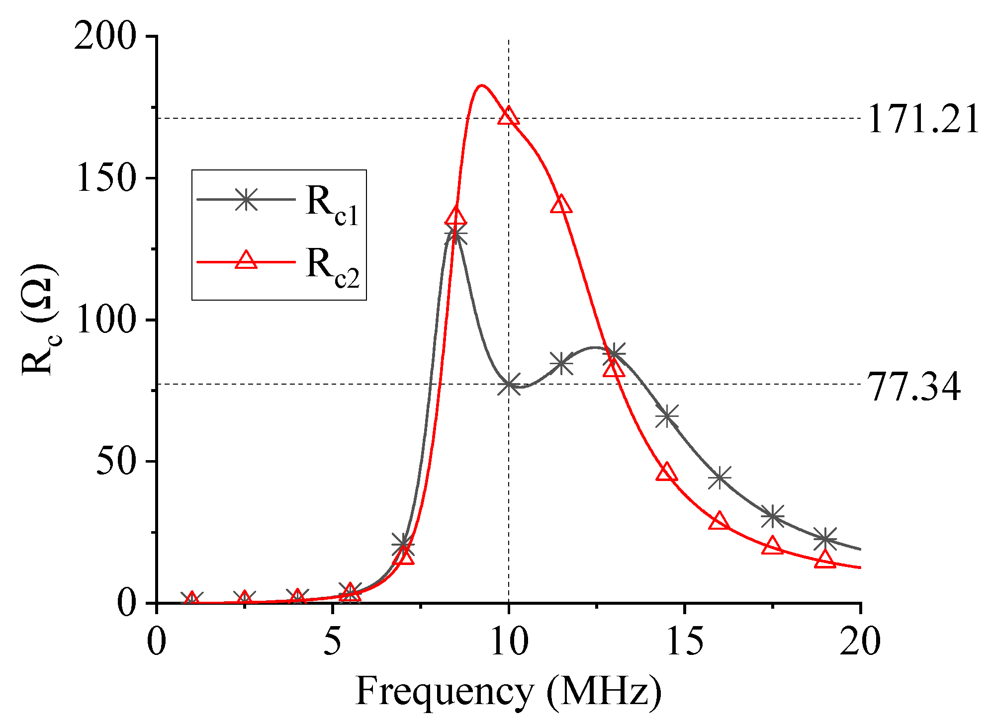
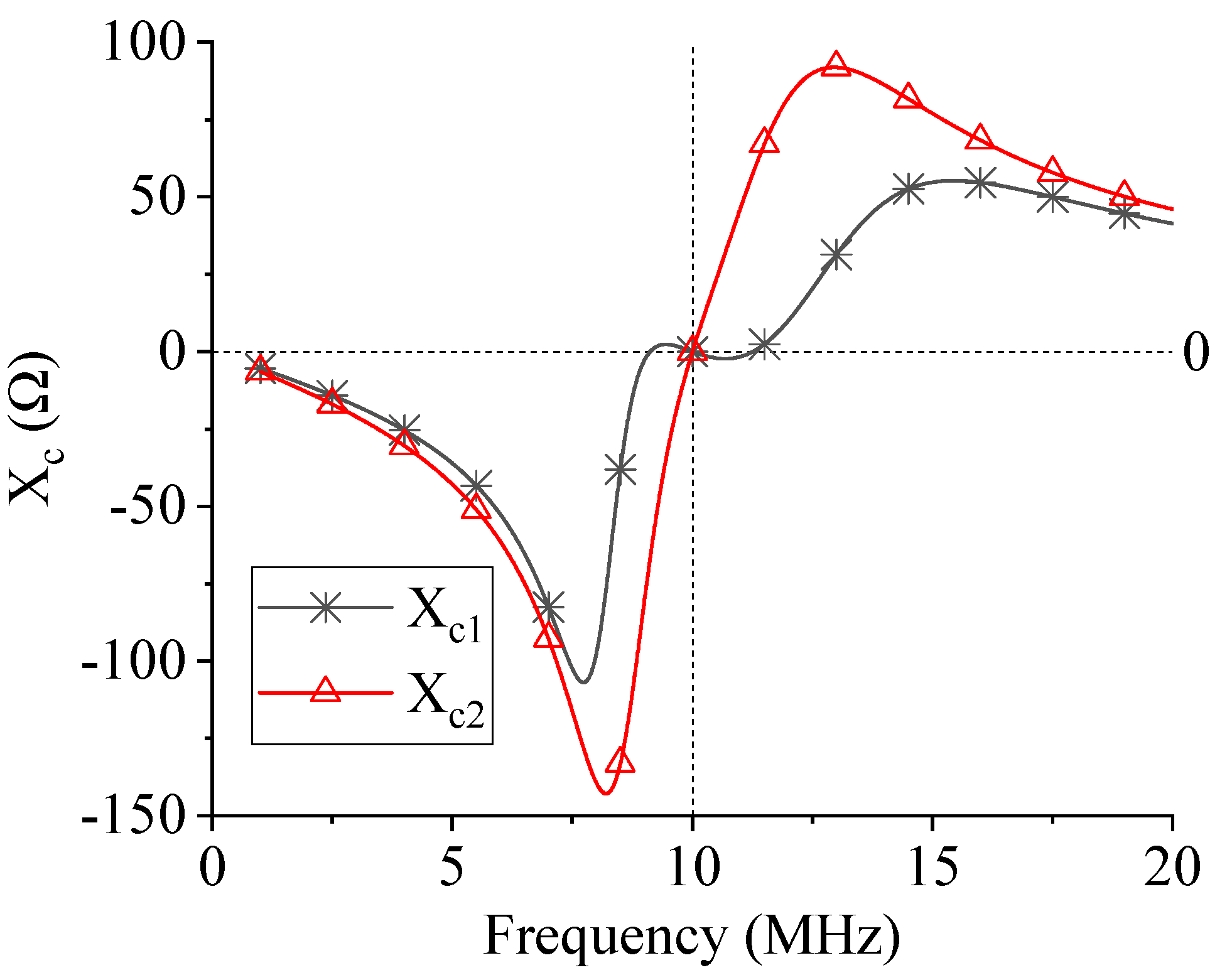
Finally, frequency simulations with a step of 5 k Hz have been performed for calculating the frequency behaviour of the conjugate image impedances of the link Z c i = R c i + j X c i = 1 / Y c i . Furthermore, in this case the figures of merit directly available in the simulator have been used. The obtained simulated data are given in Figure 7 and Figure 8. As expected, at f 0 = 10 M Hz the conjugate image impedances of the link are two simple resistors having the values provided by the analytical formulas.
In order to confirm the accuracy of the analytical results, measurements on a capacitive wireless power transfer setup with one electric field repeater are required and are part of future research. For these measurements, the dual methodology as in [18] can be applied.

6. Conclusions

A capacitive wireless power transfer system with a repeater element allows for larger power transfer distances. No cross-coupling between transmitter and receiver was assumed. First, the power gain, the available gain and the transducer gain were analytically determined as function of the network elements (Table 3). Next, the optimal load and source admittance were calculated to maximize each gain. It was found that the load should equal (42) in order to maximize the power gain G P . This corresponds to optimizing the efficiency of the WPT system. In order to maximize the available gain G A , the internal source conductance should equal (41). If both the internal source conductance and load equal (41) and (42), respectively, the transducer gain G T is maximized, resulting in a maximum power transfer to the load for a fixed source. In that case, the maximum attainable gain, called the ultimate gain G M , is achieved and is, for the CPT system with one repeater, given by (46). Finally, the analytical solution was verified by numerical simulation.

Author Contributions

Conceptualization, methodology, B.M., M.M.; validation, B.M., G.M.; writing—original draft preparation, B.M., G.M.; writing—review and editing, A.C., G.M., M.M. All authors have read and agreed to the published version of the manuscript.

Funding

This research received no external funding.

Conflicts of Interest

The authors declare no conflict of interest.

References

  1. Lu, X.; Wang, P.; Niyato, D.; Kim, D.I.; Han, Z. Wireless Charging Technologies: Fundamentals, Standards, and Network Applications. IEEE Commun. Surveys Tutor. 2015, 18, 1413–1452. [Google Scholar] [CrossRef] [Green Version]
  2. Jawad, A.M.; Nordin, R.; Gharghan, S.K.; Jawad, H.M.; Ismail, M. Opportunities and Challenges for Near-field Wireless Power Transfer: A Review. Energies 2017, 10, 1022. [Google Scholar] [CrossRef]
  3. Barman, S.D.; Reza, A.W.; Kumar, N.; Karim, M.E.; Munir, A.B. Wireless Powering by Magnetic Resonant Coupling: Recent Trends in Wireless Power Transfer System and its Applications. Renew. Sustain. Energy Rev. 2015, 51, 1525–1552. [Google Scholar] [CrossRef]
  4. Rodenbeck, C.T.; Jaffe, P.I.; Strassner, B.H., II; Hausgen, P.E.; McSpadden, J.O.; Kazemi, H.; Shinohara, N.; Tierney, B.B.; DePuma, C.B.; Self, A.P. Microwave and Millimeter Wave Power Beaming. IEEE J. Microw. 2020, 1, 229–259. [Google Scholar] [CrossRef]
  5. Chen, Q.; Chen, X.; Duan, X. Investigation on beam collection efficiency in microwave wireless power transmission. J. Electromagn. Waves Appl. 2018, 32, 1136–1151. [Google Scholar] [CrossRef]
  6. Dickinson, R.M. Wireless power transmission technology state of the art the first Bill Brown lecture. Acta Astron. 2003, 53, 561–570. [Google Scholar] [CrossRef]
  7. Summerer, L.; Purcell, O. Concepts for wireless energy transmission via laser. In Proceedings of the Europeans Space Agency (ESA)-Advanced Concepts Team, International Conference on Space Optical Systems and Applications (ICSOS), Tokyo, Japan, 4–6 February 2009. [Google Scholar]
  8. Dai, J.; Ludois, D.C. Wireless electric vehicle charging via capacitive power transfer through a conformal bumper. In Proceedings of the IEEE Applied Power Electronics Conf. and Exposition (APEC), Charlotte, NC, USA, 15–19 March 2015; pp. 3307–3313. [Google Scholar]
  9. Miyazaki, M.; Abe, S.; Suzuki, Y.; Sakai, N.; Ohira, T.; Sugino, M. Sandwiched parallel plate capacitive coupler for wireless power transfer tolerant of electrode displacement. In Proceedings of the IEEE MTT-S International Conference on Microwaves for Intelligent Mobility (ICMIM), Nagoya, Japan, 19–21 March 2017; pp. 29–32. [Google Scholar]
  10. Sodagar, A.M.; Amiri, P. Capacitive coupling for power and data telemetry to implantable biomedical microsystems. In Proceedings of the 4th International IEEE/EMBS Conf. on Neural Engineering, Antalya, Turkey, 29 April–2 May 2009; pp. 411–414. [Google Scholar]
  11. Culurciello, E.; Andreou, A.G. Capacitive inter-chip data and power transfer for 3-D VLSI. IEEE Trans. Circuits Syst. II Express Briefs 2006, 53, 1348–1352. [Google Scholar] [CrossRef]
  12. Theodoridis, M.P. Effective capacitive power transfer. IEEE Trans. Power Electron. 2012, 27, 4906–4913. [Google Scholar] [CrossRef]
  13. Lu, F.; Zhang, H.; Mi, C. A Review on the Recent Development of Capacitive Wireless Power Transfer Technology. Energies 2017, 10, 1752. [Google Scholar] [CrossRef] [Green Version]
  14. Minnaert, B.; Stevens, N. Conjugate Image Theory Applied on Capacitive Wireless Power Transfer. Energies 2017, 10, 46. [Google Scholar] [CrossRef] [Green Version]
  15. Kumar, A.; Pervaiz, S.; Chang, C.K.; Korhummel, S.; Popovic, Z.; Afridi, K.K. Investigation of Power Transfer Density Enhancement in Large Air-gap Capacitive Wireless Power Transfer Systems. In Proceedings of the IEEE Wireless Power Transfer Conference, Boulder, CO, USA, 13–15 May 2015; pp. 1–4. [Google Scholar]
  16. Zhang, H.; Lu, F.; Hofmann, H.; Liu, W.; Mi, C.C. An LC-compensated Electric Field Repeater for Long-distance Capacitive Power Transfer. IEEE Trans. Ind. Appl. 2017, 53, 4914–4922. [Google Scholar] [CrossRef]
  17. Ahn, D.; Hong, S. A Study on Magnetic Field Repeater in Wireless Power Transfer. IEEE Trans. Ind. Electron. 2012, 60, 360–371. [Google Scholar] [CrossRef]
  18. Zhang, Y.; Lu, T.; Zhao, Z.; Chen, K.; He, F.; Yuan, L. Wireless Power Transfer to Multiple Loads over Various Distances using Relay Resonators. IEEE Microw. Wireless Compon. Lett. 2015, 25, 337–339. [Google Scholar] [CrossRef]
  19. Kim, J.; Son, H.C.; Kim, K.H.; Park, Y.J. Efficiency Analysis of Magnetic Resonance Wireless Power Transfer with Intermediate Resonant Coil. IEEE Antennas Wirel. Propag. Lett. 2011, 10, 389–392. [Google Scholar] [CrossRef]
  20. Monti, G.; Corchia, L.; Tarricone, L.; Mongiardo, M. A Network Approach for Wireless Resonant Energy Links using Relay Resonators. IEEE Trans. Microw. Theory Tech. 2016, 64, 3271–3279. [Google Scholar] [CrossRef]
  21. Mastri, F.; Mongiardo, M.; Monti, G.; Dionigi, M.; Tarricone, L. Gain Expressions for Resonant Inductive Wireless Power Transfer Links with One Relay Element. Wireless Power Transfer 2018, 5, 27–41. [Google Scholar] [CrossRef]
  22. Egan, W.F. Practical RF System Design; John Wiley & Sons: Hoboken, NJ, USA, 2003; pp. 313–315. [Google Scholar]
  23. Wang, Q.; Che, W.; Dionigi, M.; Mastri, F.; Mongiardo, M.; Monti, G. Gains Maximization via Impedance Matching Networks for Wireless Power Transfer. Prog. Electromagn. Res. 2019, 164, 135–153. [Google Scholar] [CrossRef] [Green Version]
  24. Maddock, R.J. Fundamentals of Network Analysis. In Intermediate Electronics; Springer: Boston, MA, USA, 1969; p. 66. [Google Scholar]
  25. Roberts, S. Conjugate-image Impedances. Proc. IRE 1946, 34, 198–204. [Google Scholar] [CrossRef]
  26. Hong, J.S.G.; Lancaster, M.J. Microstrip Filters for RF/Microwave Applications; John Wiley & Sons: Hoboken, NJ, USA, 2004; Volume 167. [Google Scholar]
  27. Minnaert, B.; Stevens, N. Optimal analytical solution for a capacitive wireless power transfer system with one transmitter and two receivers. Energies 2017, 10, 1444. [Google Scholar] [CrossRef] [Green Version]
Figure 1. A capacitive wireless power transfer system with one electric field repeater, consisting of capacitor plates, a compensation network, and resistive losses.
Electronics 10 00723 g001
Figure 2. (a) The capacitive link connected to a source and a load. The input power P i n and load power P L are defined in the figure. (b) The Norton equivalent circuit of the system at the load port and definition of the maximum available load power P A (c) Definition of the available input power P A G of the generator.
Electronics 10 00723 g002
Figure 3. Definition of the conjugate image admittances Y c 1 and Y c 2 .
Electronics 10 00723 g003
Figure 4. Equivalent circuit of the capacitive wireless power transfer system with one electric field repeater. Energy is wirelessly transferred from the transmitter (on the left) via the electric field repeater (in the middle) to the receiver (at the right).
Electronics 10 00723 g004
Figure 5. Results obtained for the analyzed numerical example by varying R L . The figure shows the simulated gains.
Electronics 10 00723 g005
Figure 6. Results obtained for the analyzed numerical example by varying the internal source impedance R S . The figure shows the simulated gains.
Electronics 10 00723 g006
Figure 7. Results obtained for the frequency behaviour of R c i .
Electronics 10 00723 g007
Figure 8. Results obtained for the frequency behaviour of X c i .
Electronics 10 00723 g008
Table 1. Definition and expressions for the different types of gain for a general loaded two-port network. Y c 1 and Y c 2 are given by (24) and (25).
GainDefinitionGeneral Two-PortMaximum If
G P P L P i n G L G i n | y 21 y 22 + Y L | 2 Y L = Y c 2
G A P A P A G G S G o u t | y 21 y 11 + Y S | 2 Y S = Y c 1
G T P L P A G 4 G L G S | y 21 ( y 11 + Y S ) ( y 22 + Y L ) y 12 y 21 | 2 Y S = Y c 1 and Y L = Y c 2
Table 2. Overview of the different parameters.
k i j = C i j C i C j B 0 = ω 0 C 2 χ i j = Q i Q j k i j
Q i = ω 0 C i G i n i j = C i C j χ 1 T 3 = Q 1 T Q 3 k 13
Q S = ω 0 C 1 G S Q 1 T = Q 1 Q S Q 1 + Q S χ 32 T = Q 3 Q 2 T k 32
Q L = ω 0 C 2 G L Q 2 T = Q 2 Q L Q 2 + Q L
Table 3. Expressions for the different gains for a capacitive wireless power transfer system with one repeater.
GainDefinitionCPT System with One Repeater
G P P L P i n χ 13 2 χ 32 T 2 ( 1 + χ 32 T 2 ) ( 1 + χ 13 2 + χ 32 T 2 ) · Q 2 T Q L
G A P A P A G Q 1 T Q S · χ 1 T 3 2 χ 23 2 ( 1 + χ 1 T 3 2 ) ( 1 + χ 23 2 + χ 1 T 3 2 )
G T P L P A G Q 1 T Q S · 4 χ 1 T 3 2 χ 32 T 2 ( 1 + χ 1 T 3 2 + χ 32 T 2 ) 2 · Q 2 T Q L
Table 4. Given parameters for the example CPT system with one repeater.
QuantityValueQuantityValue
G 1 1.50 mS C 1 300 pF
G 2 1.00 mS C 2 250 pF
G 3 2.00 mS C 3 350 pF
C 13 150 pF f 0 10.0 MHz
C 23 100 pF
Table 5. Calculated parameter values for the simulated CPT system with one repeater.
QuantityValueQuantityValue
L 1 0.844  μ H G c 1 ( R c 1 ) 12.93 mS (77.34 Ω )
L 2 1.013  μ H G c 2 ( R c 2 ) 5.841 mS (171.21 Ω )
L 3 0.724  μ H G M 56.05%
k 13 46.3%
k 23 33.8%
Publisher’s Note: MDPI stays neutral with regard to jurisdictional claims in published maps and institutional affiliations.