
Light-Load Efficiency Improvement for Ultrahigh Step-Down Converter Based on Skip Mode


Abstract
:1. Introduction
1.1. Motivation and Incitement
1.2. Literature Review
1.3. Contribution and Paper Organization
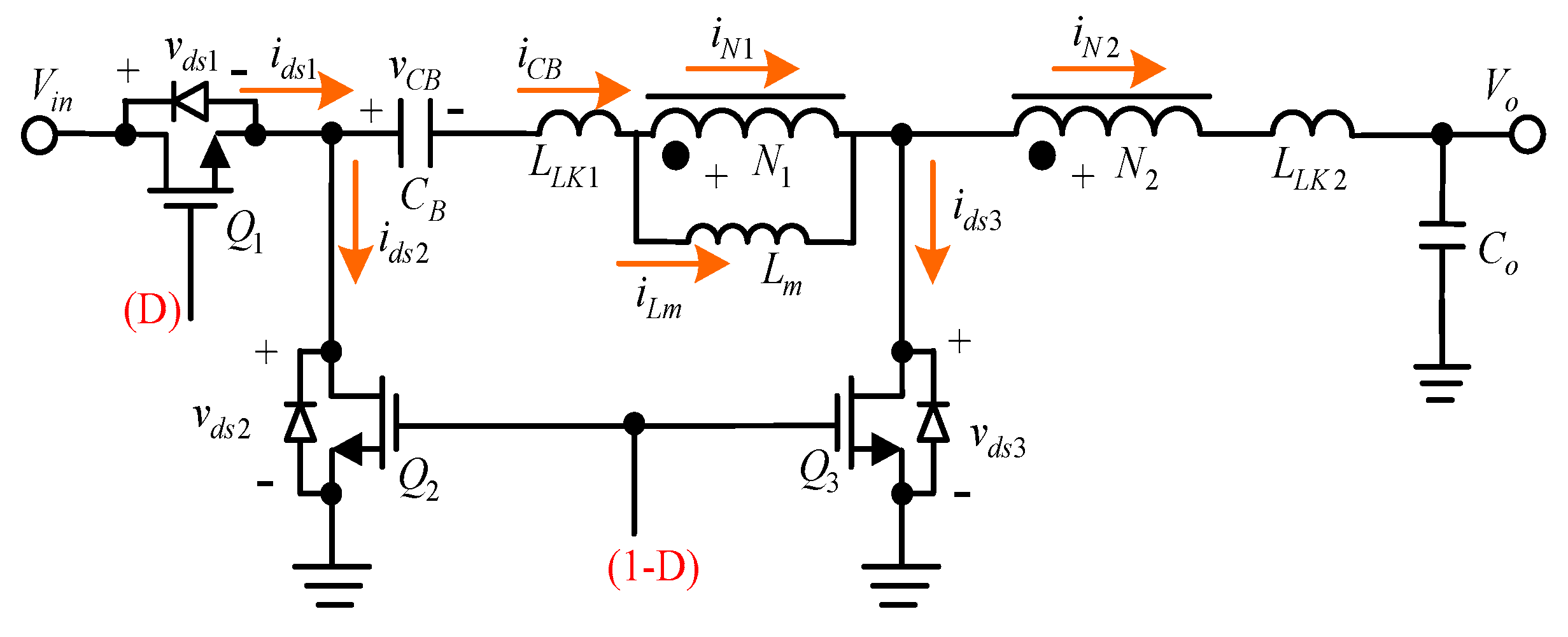
2. Used Circuit
3. Basic Circuit Operating Principles
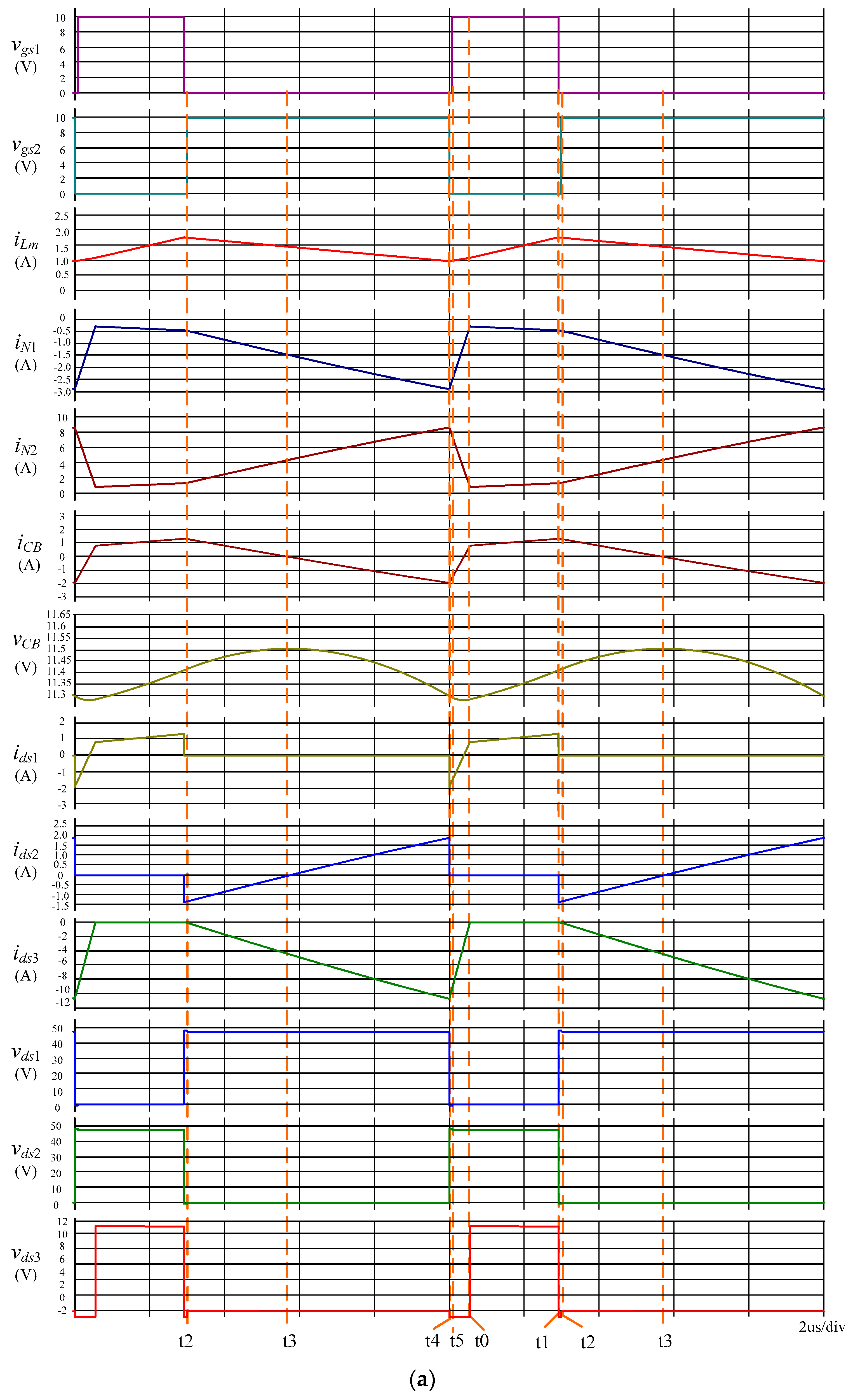
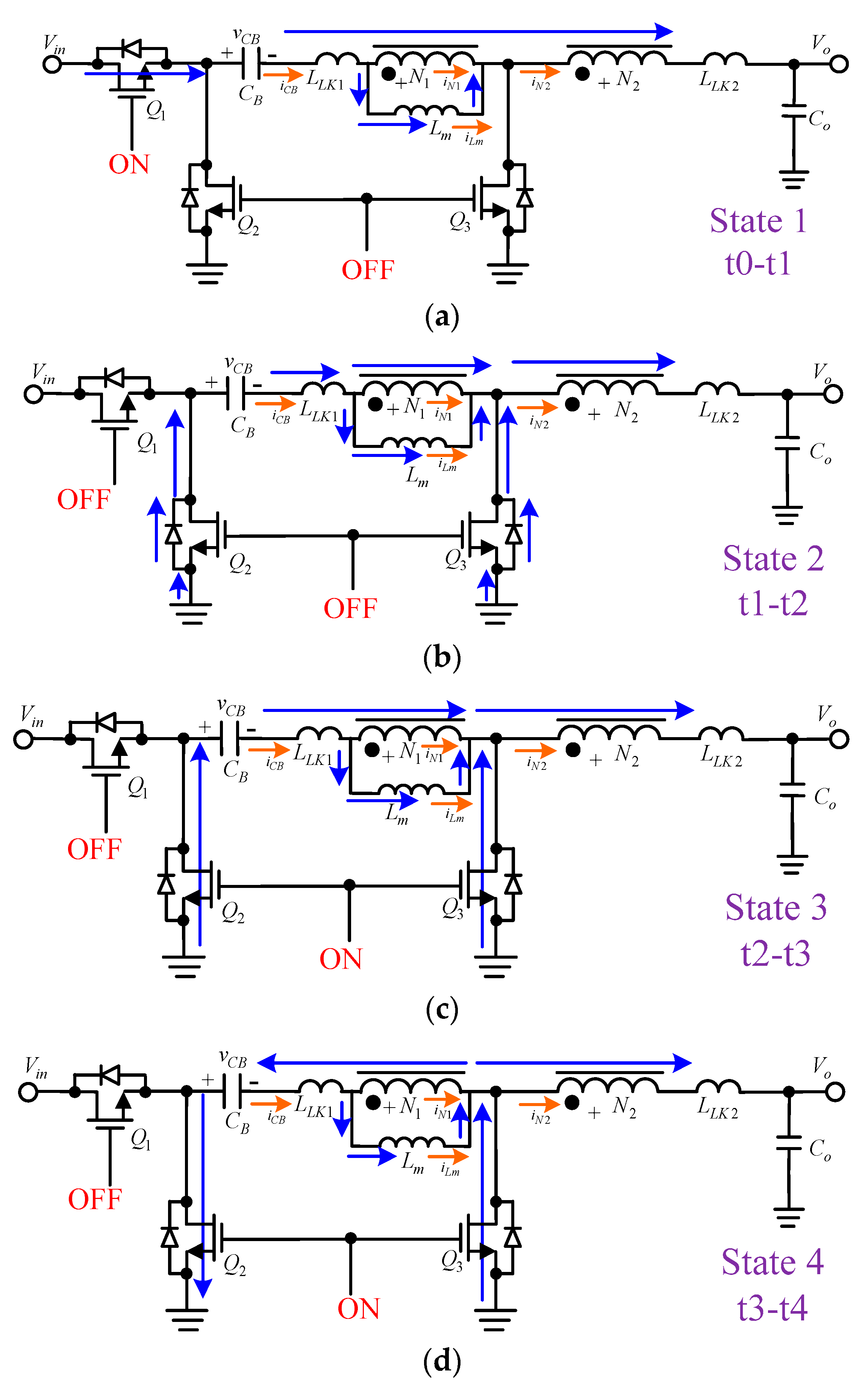
3.1. Normal Mode
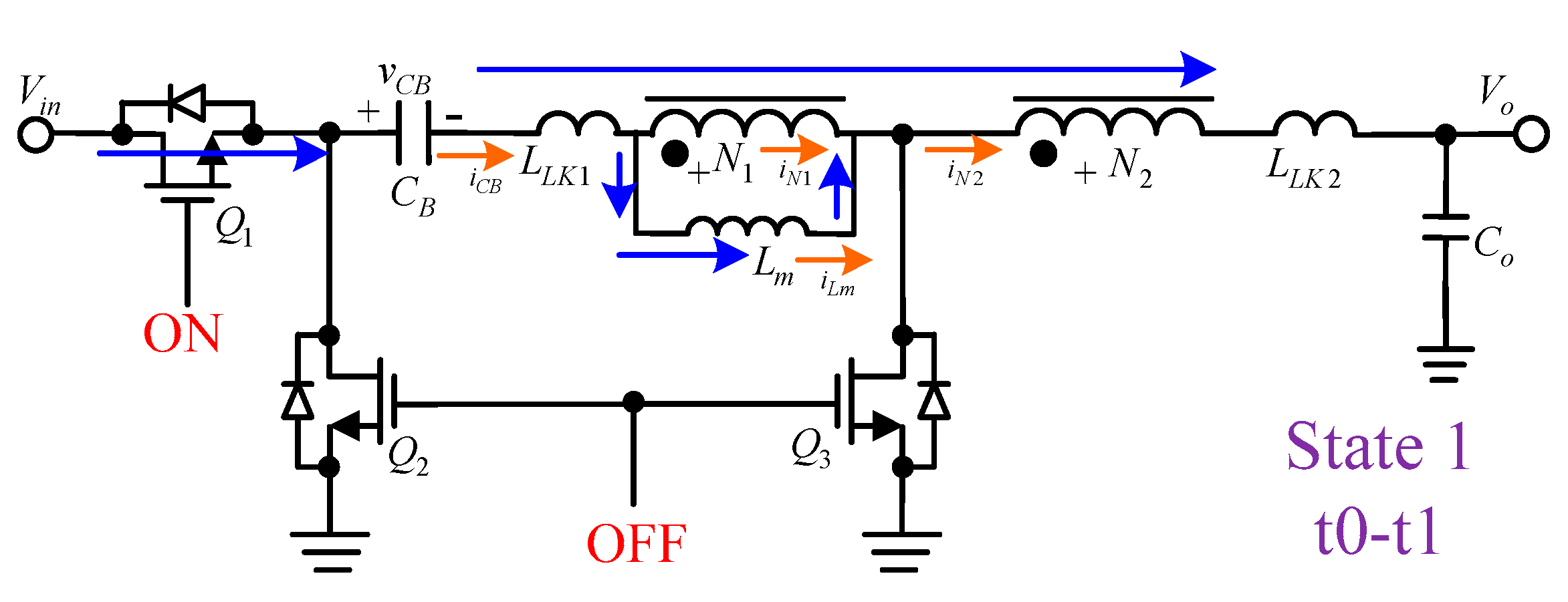
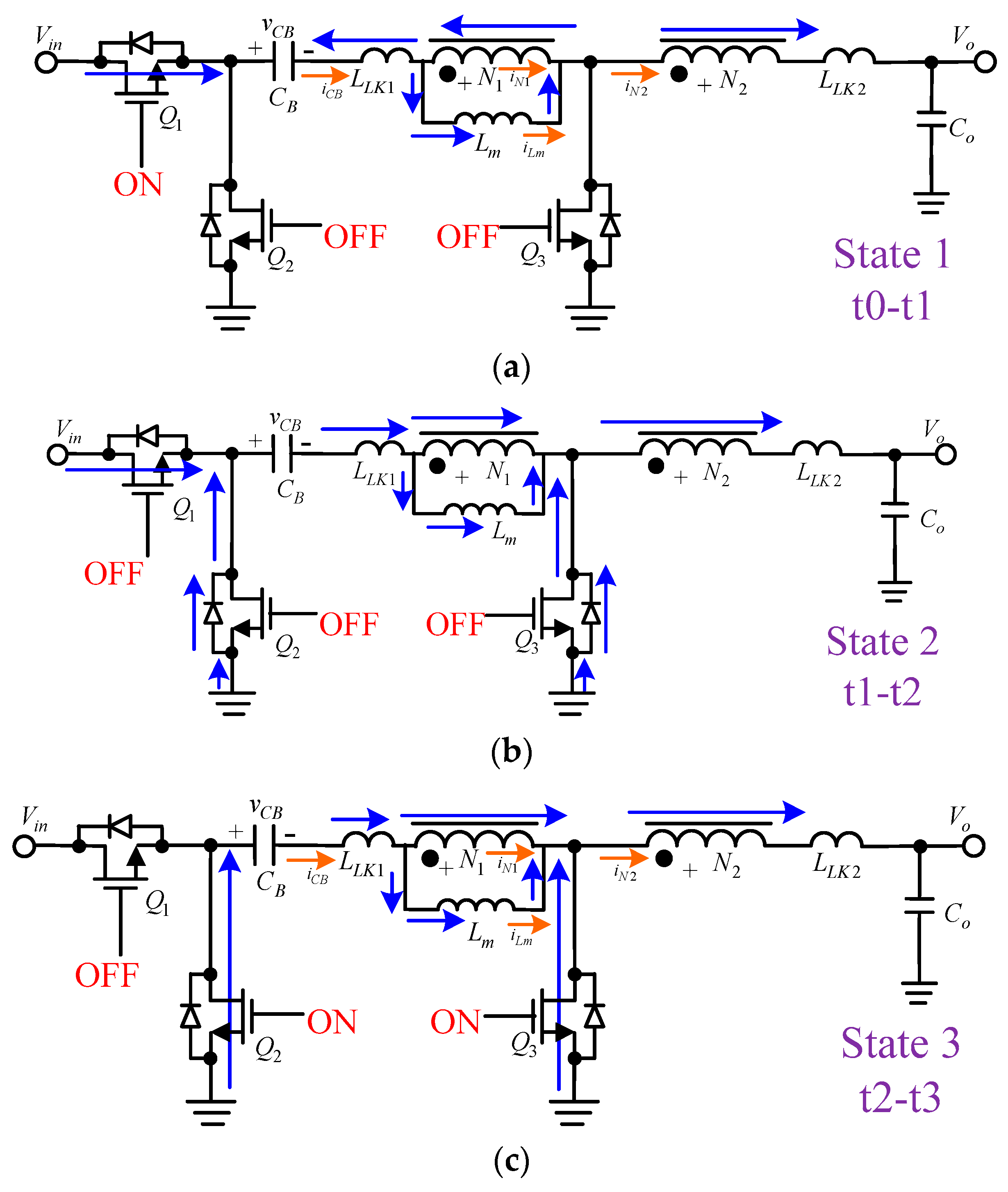
3.1.1. State 1
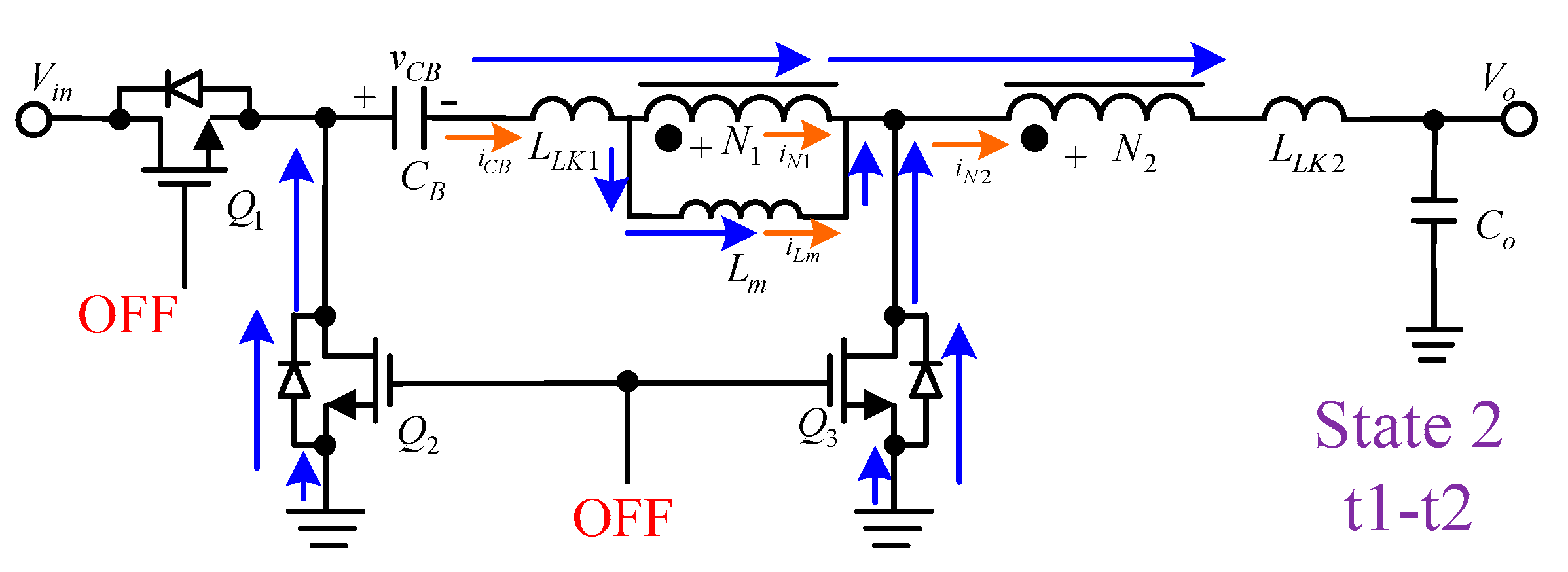
3.1.2. State 2
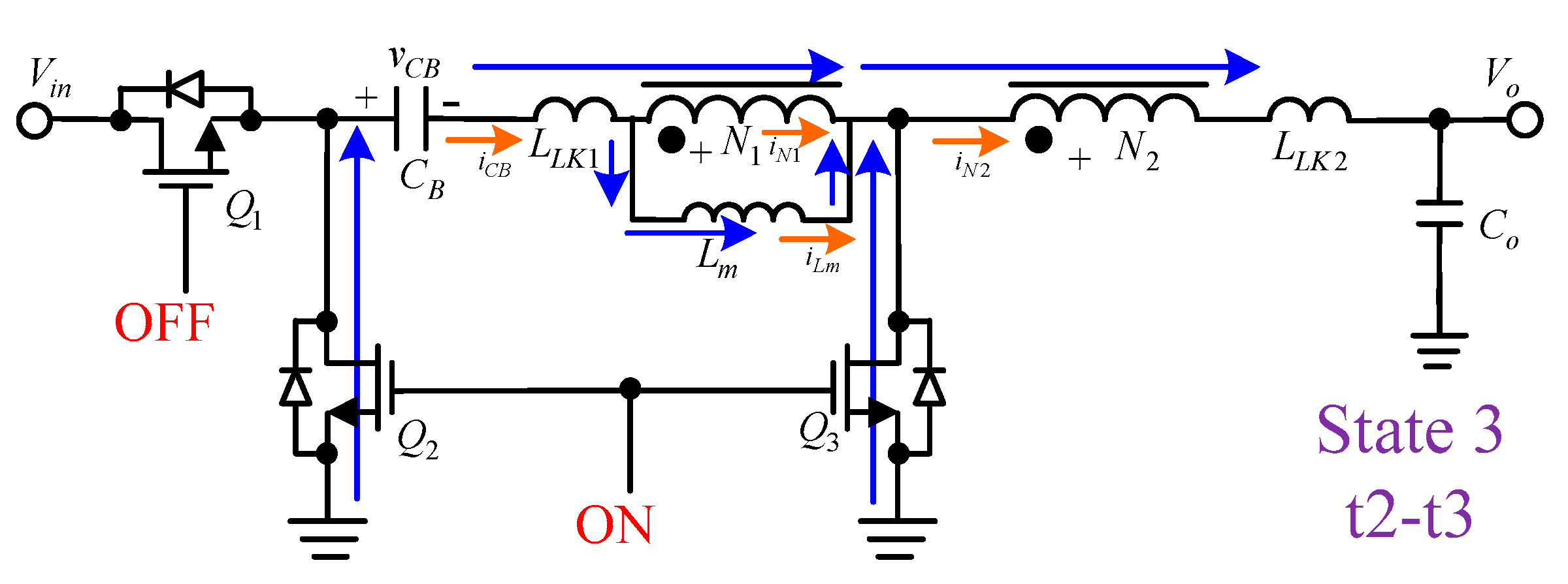
3.1.3. State 3
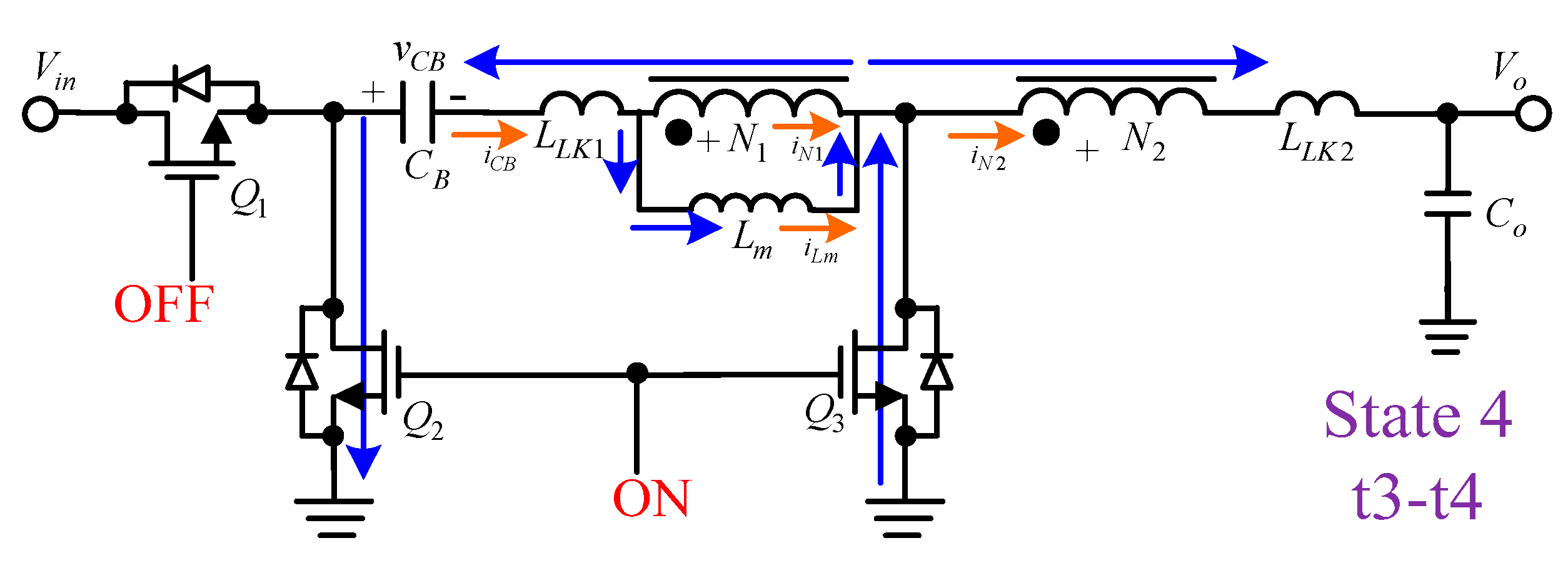
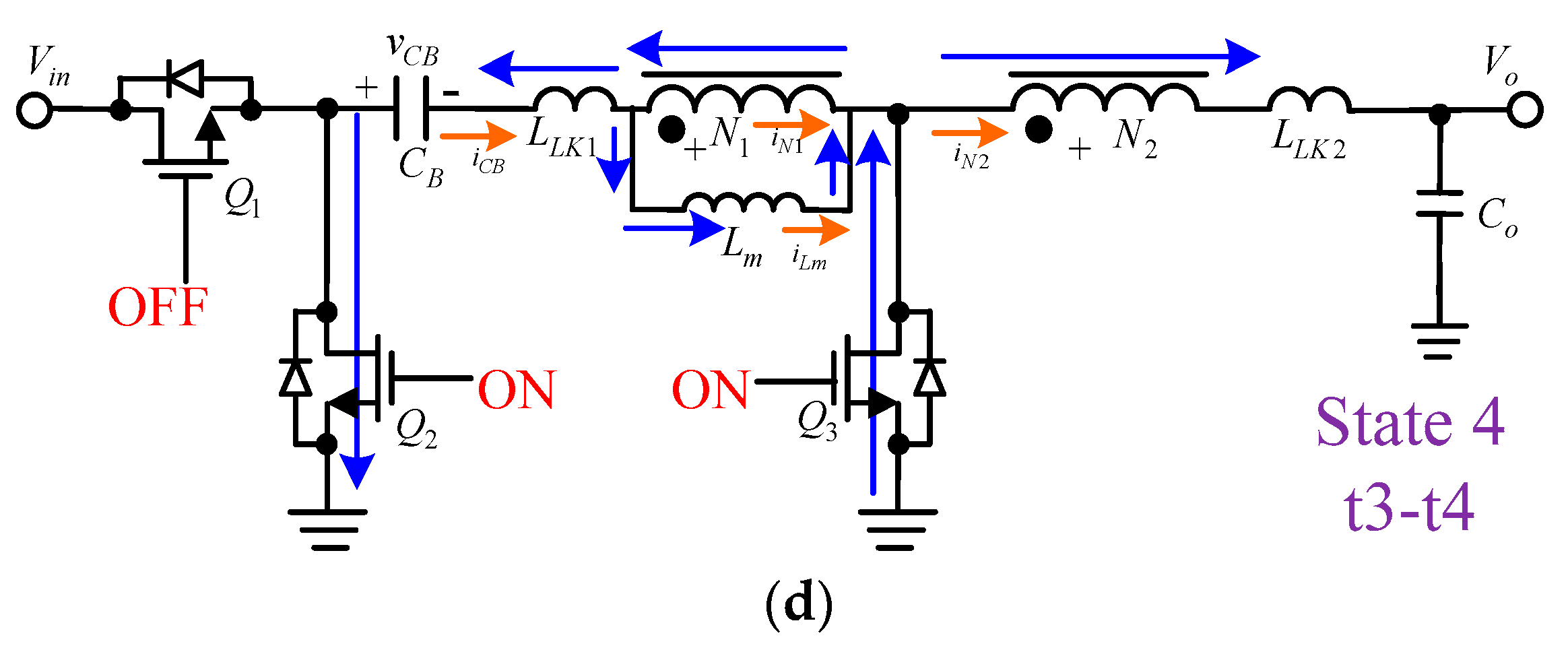
3.1.4. State 4
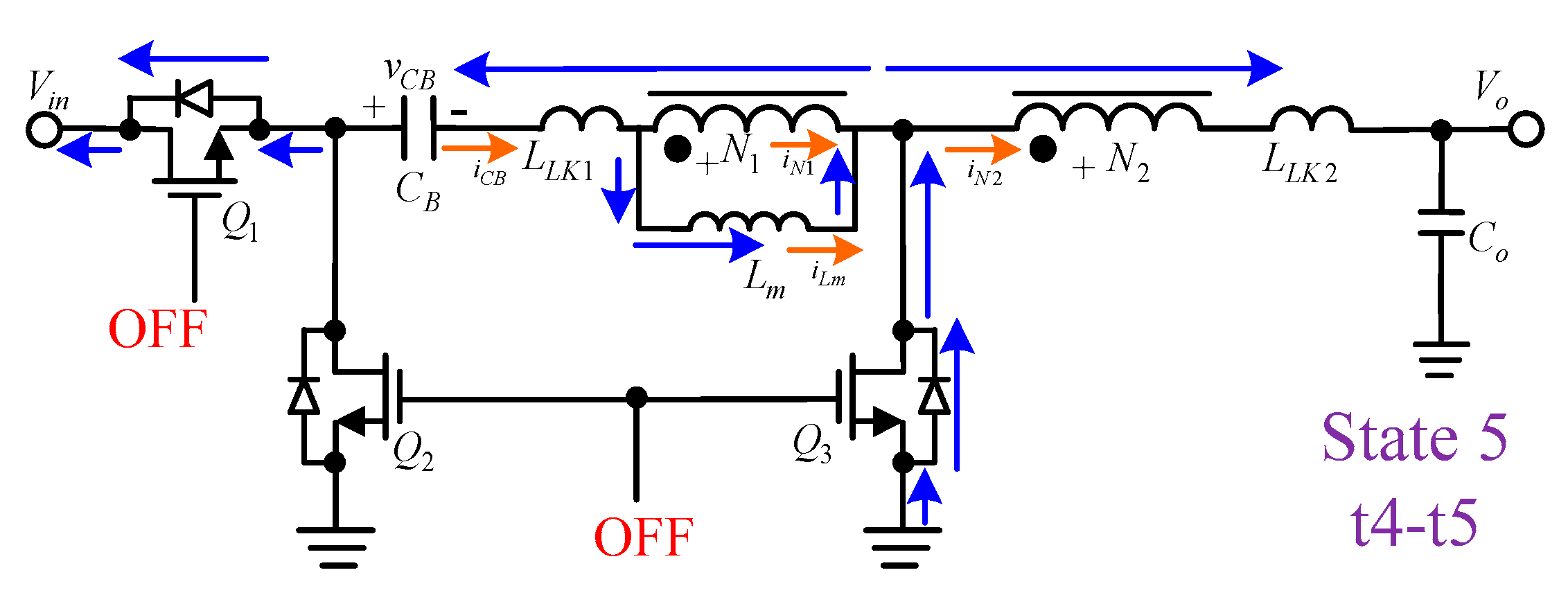
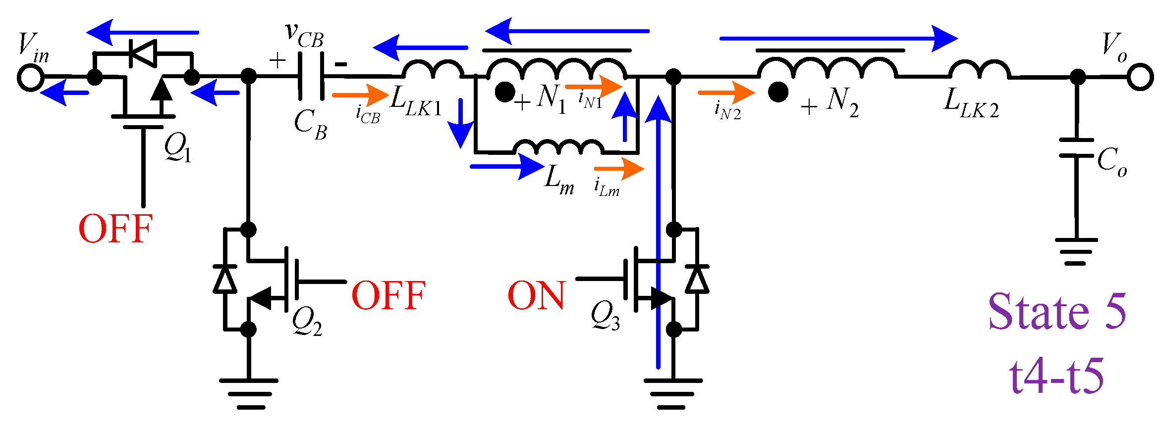
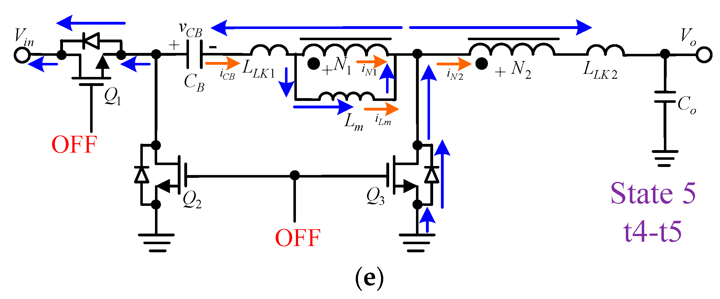
3.1.5. State 5
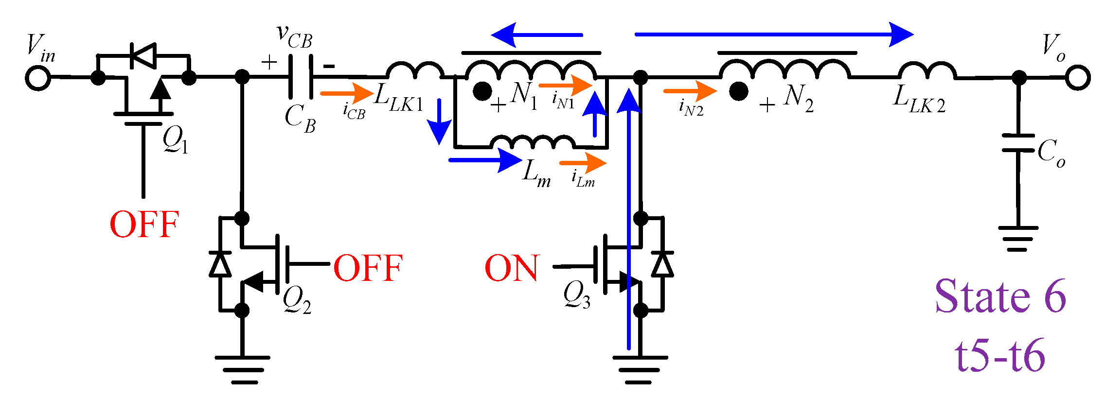
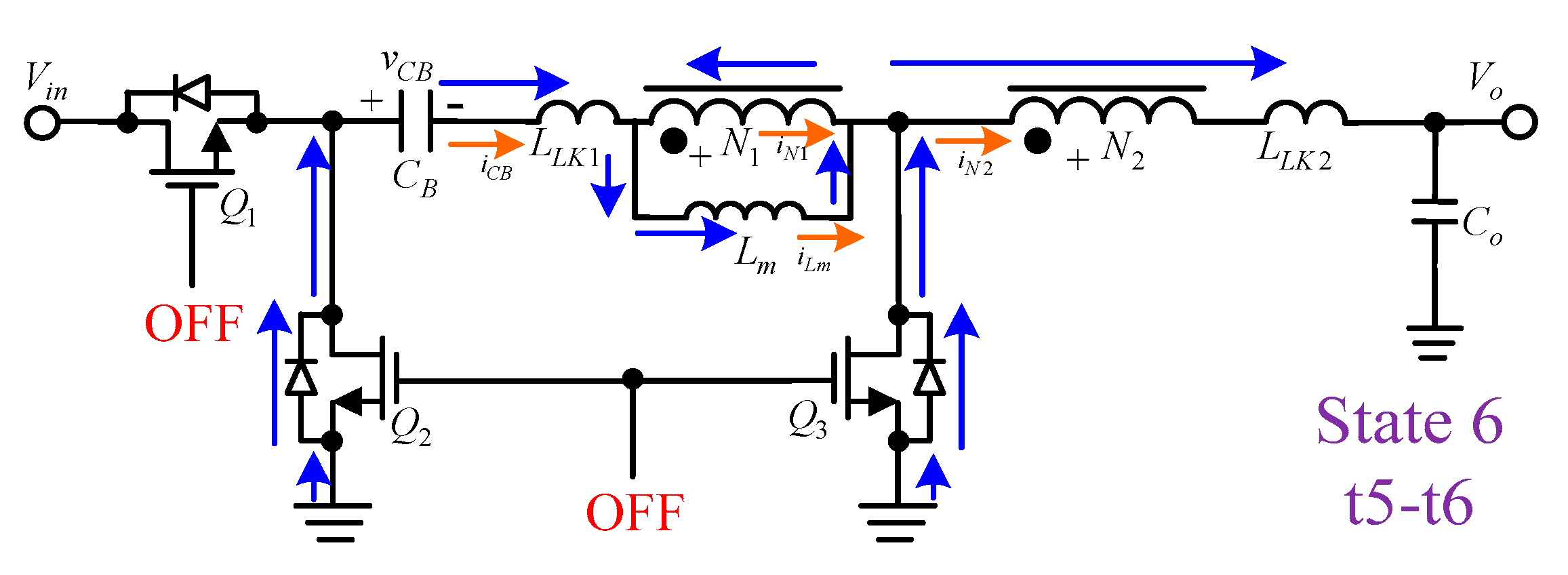
3.1.6. State 6
3.2. Skip Mode 1
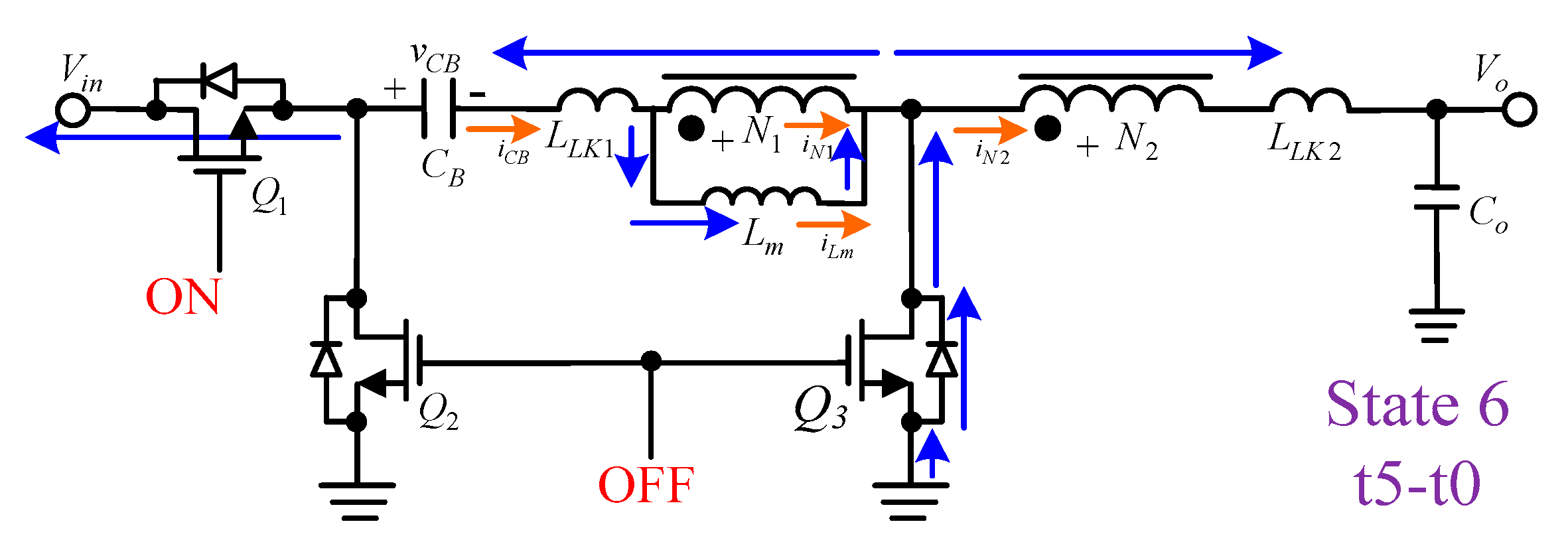
3.2.1. State 6
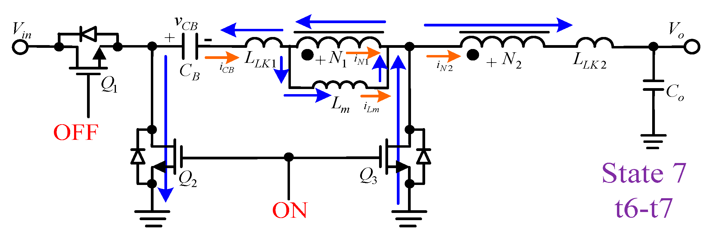
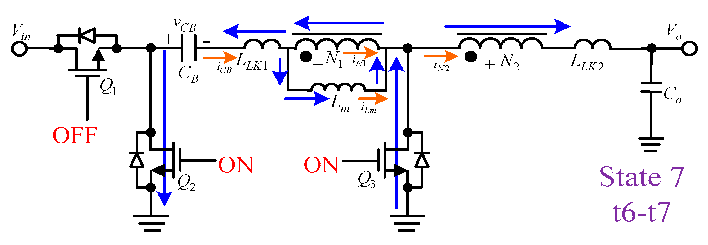
3.2.2. State 7
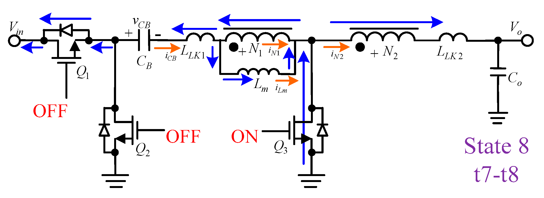
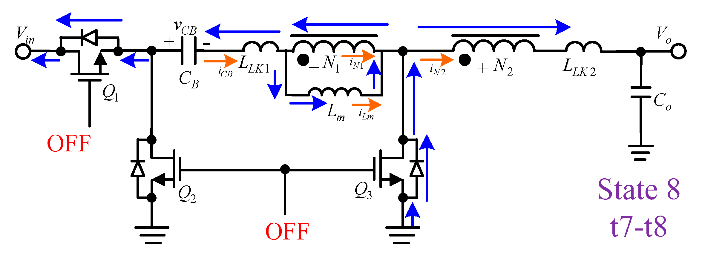
3.2.3. State 8
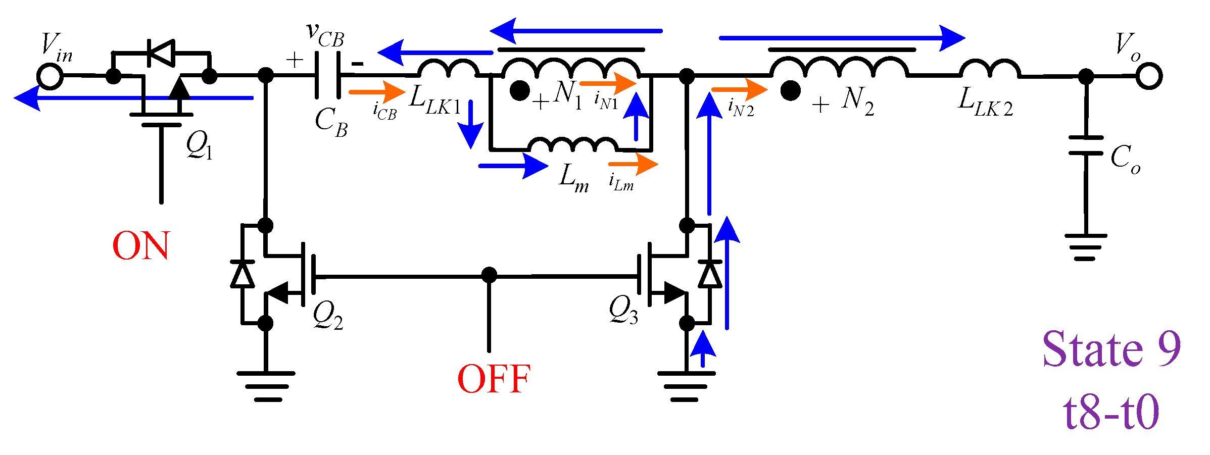
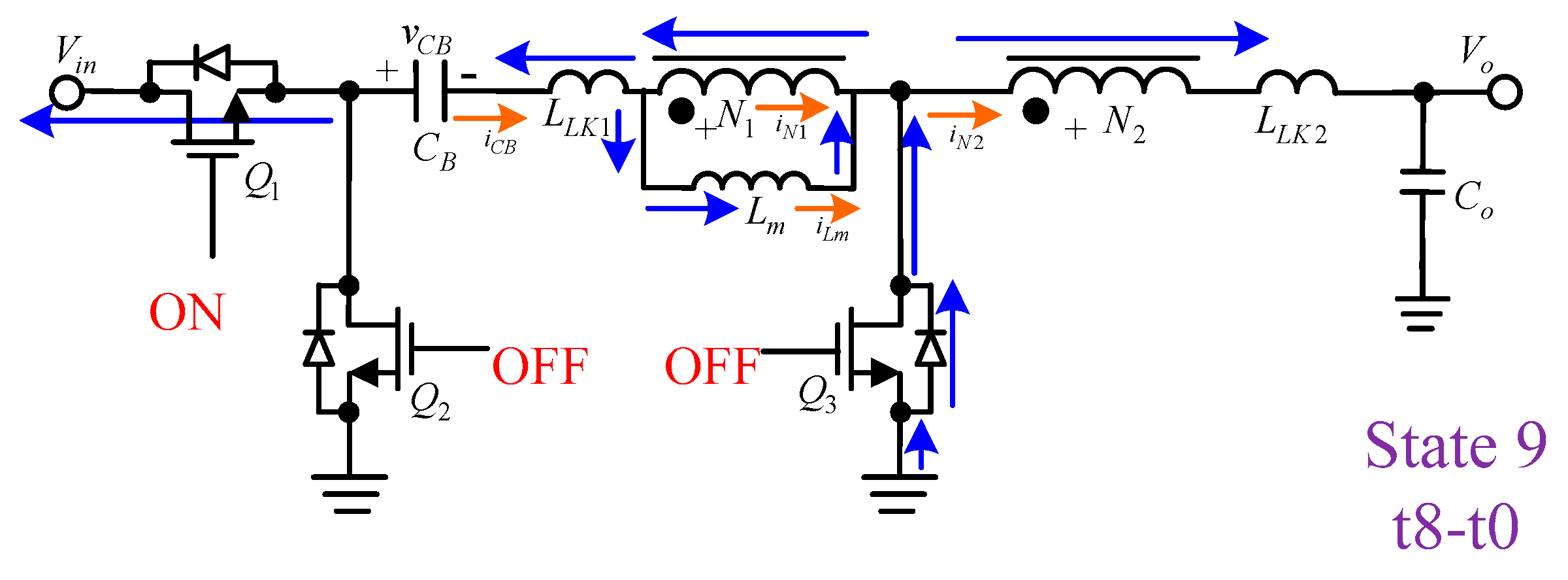
3.2.4. State 9
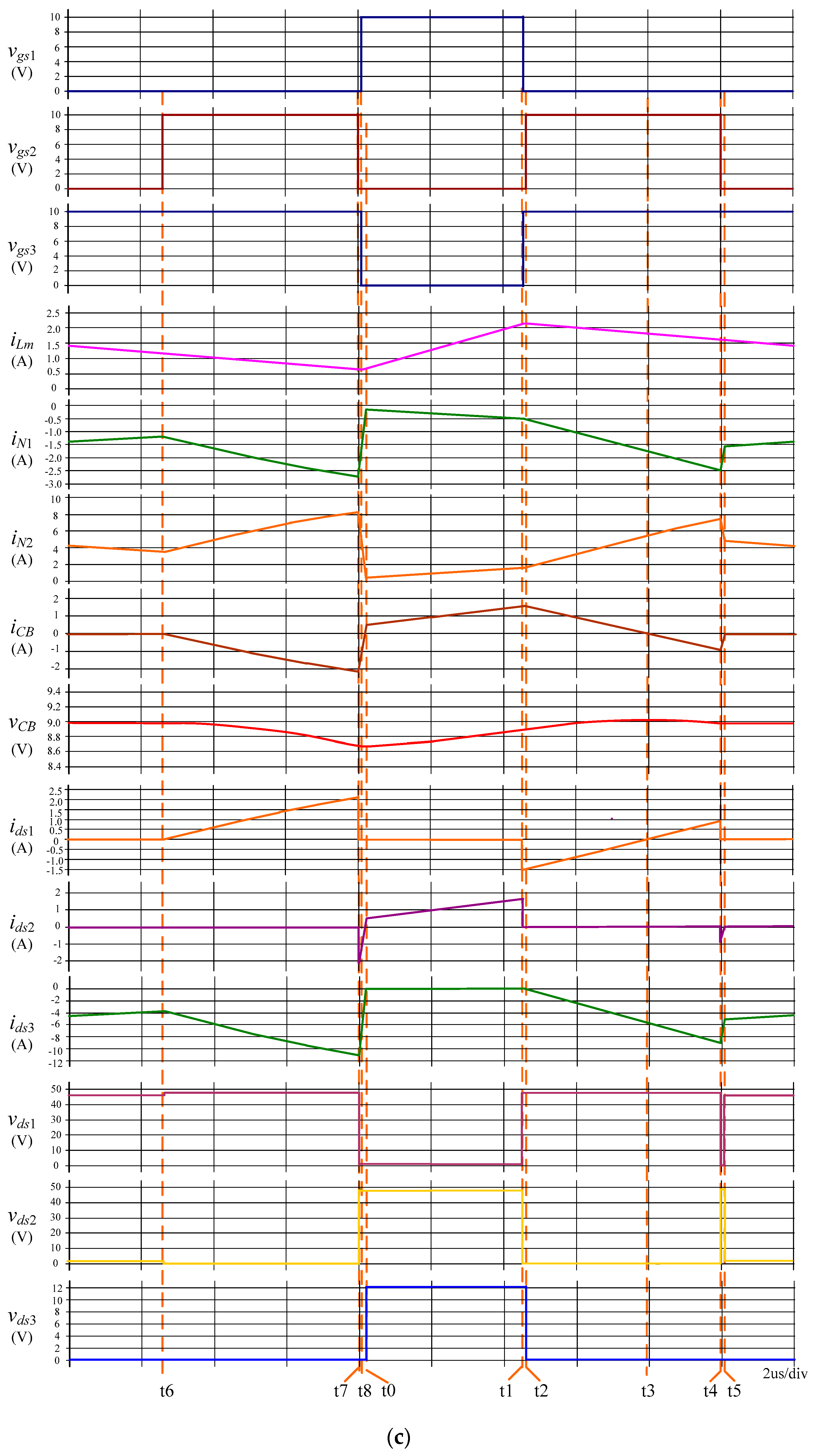
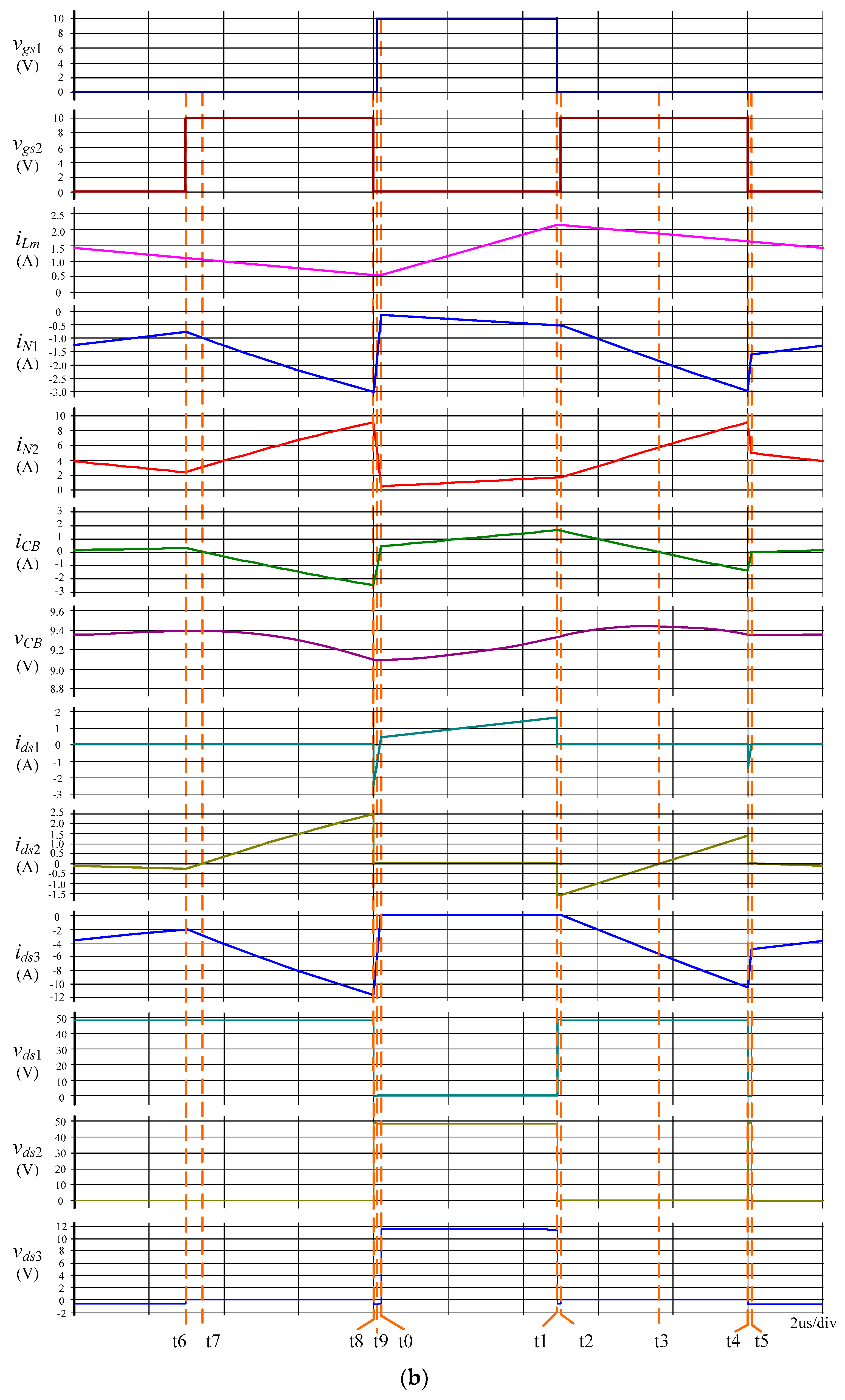
3.3. Skip Mode 2
3.3.1. State 5
3.3.2. State 6
3.3.3. State 7
3.3.4. State 8
3.3.5. State 9
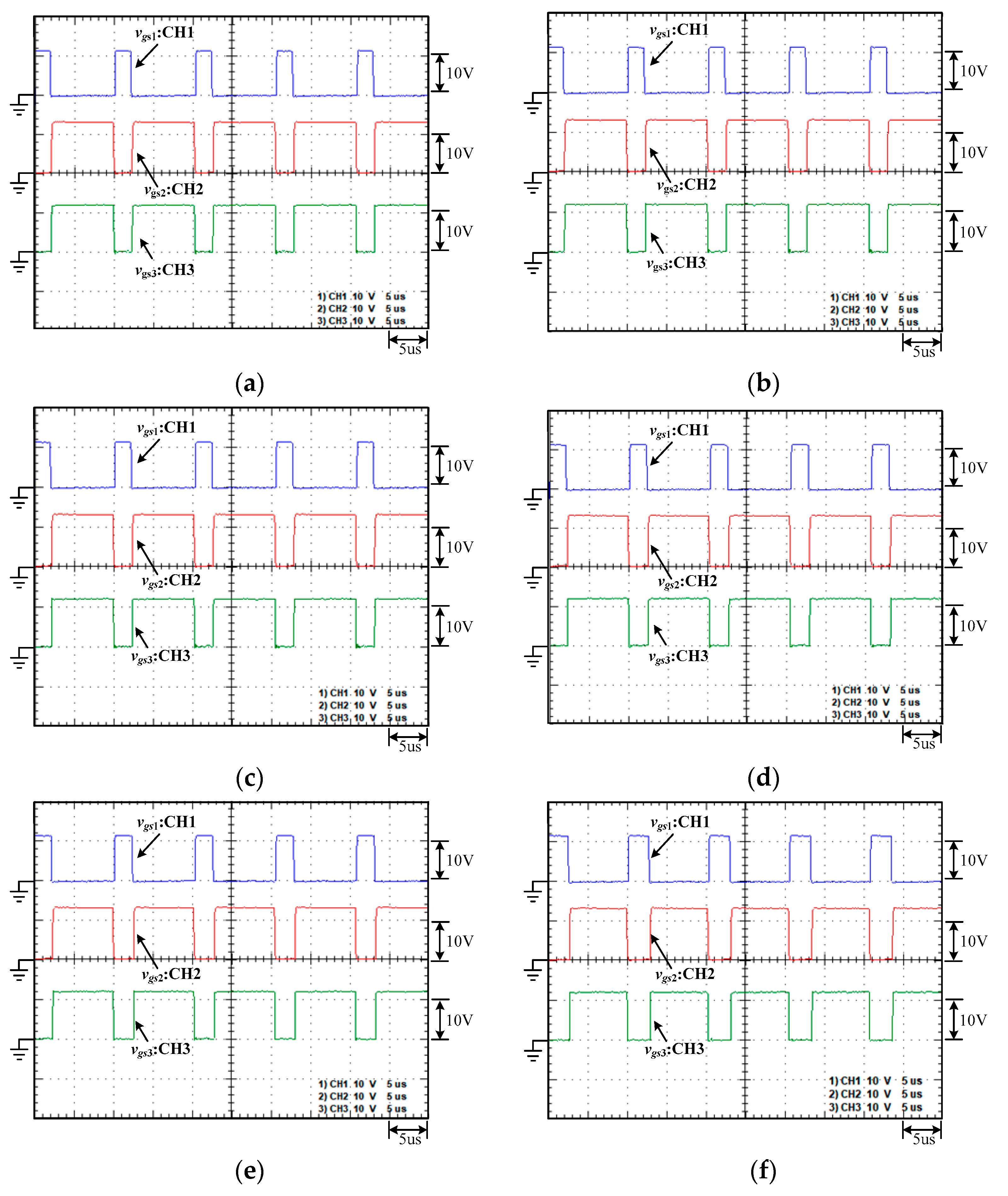
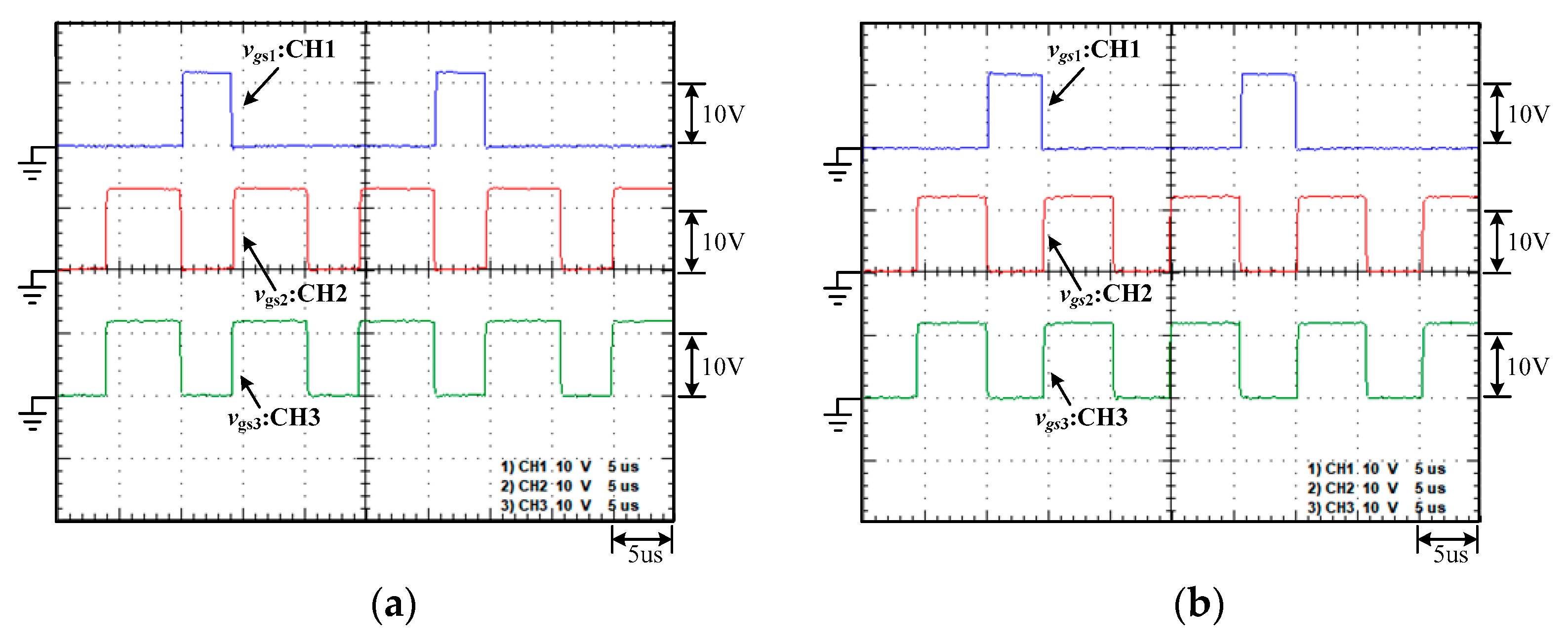
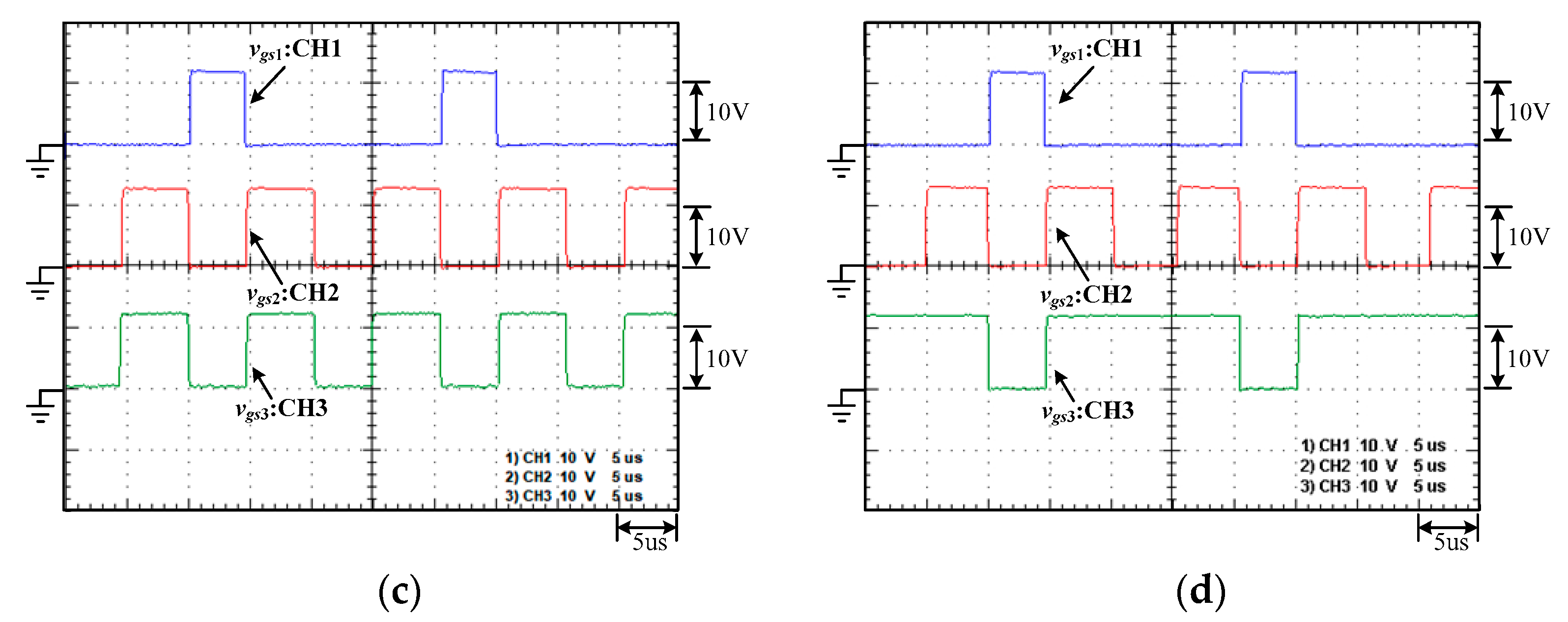
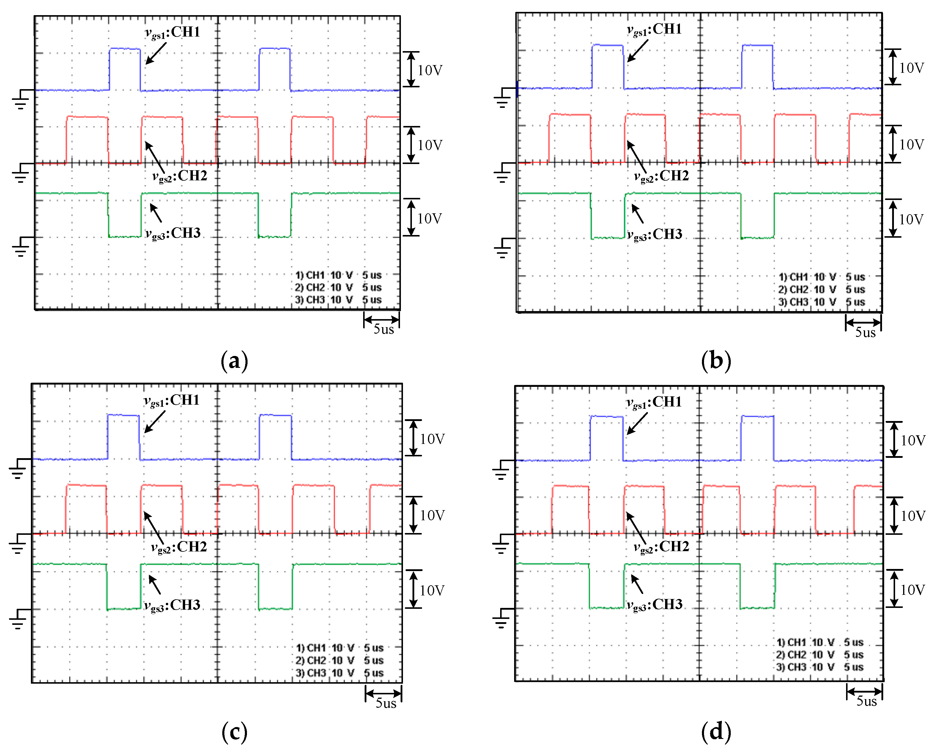
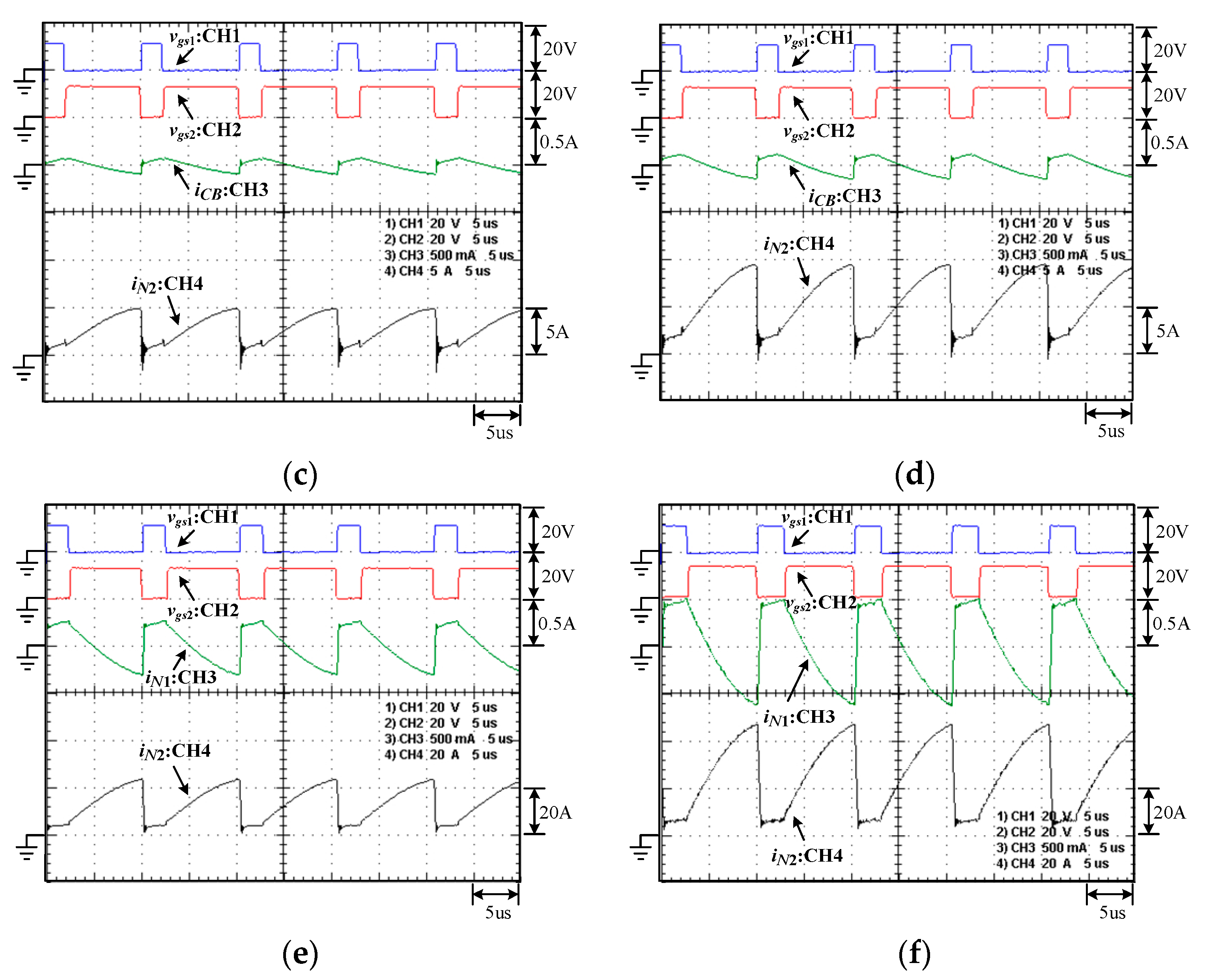
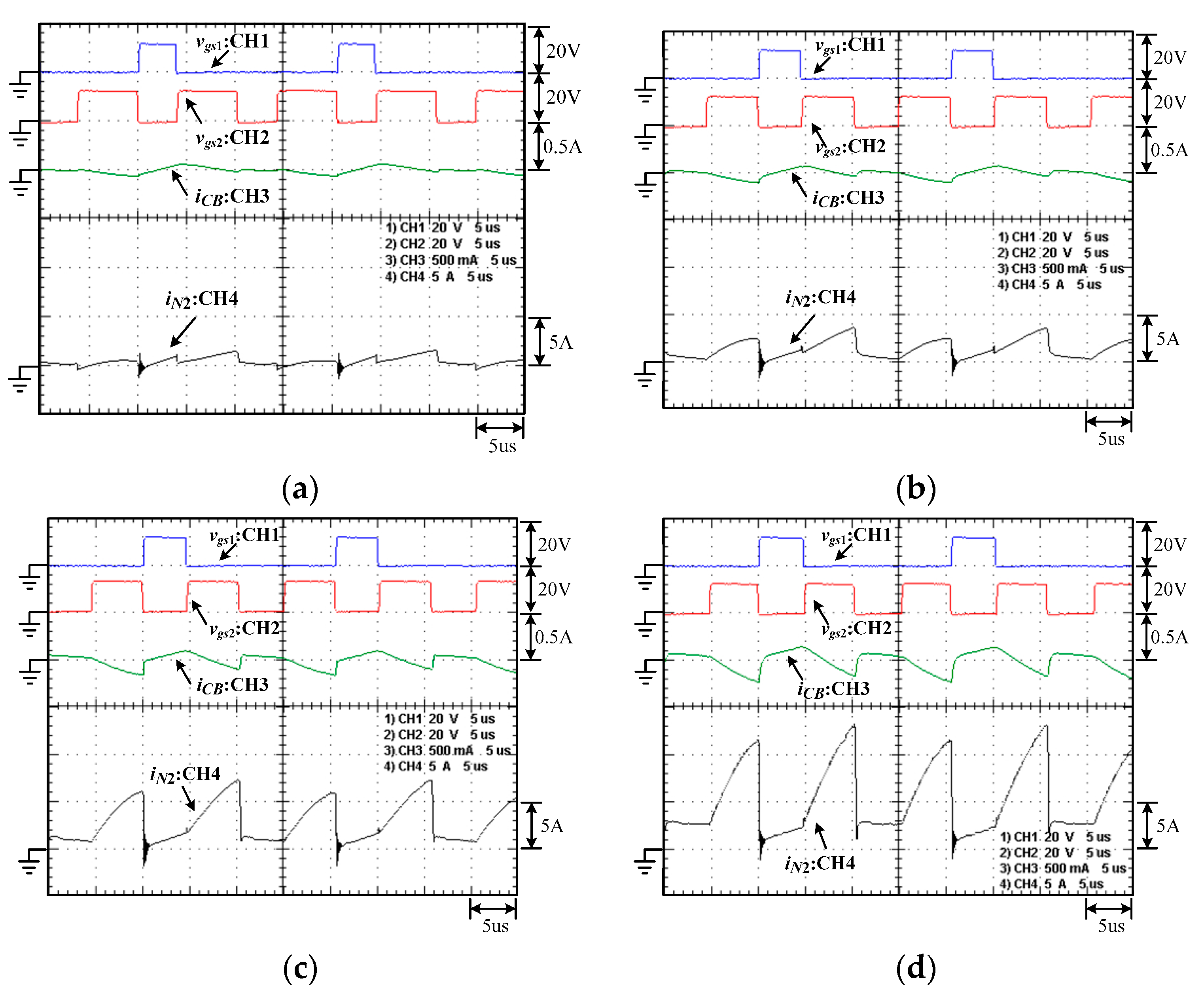
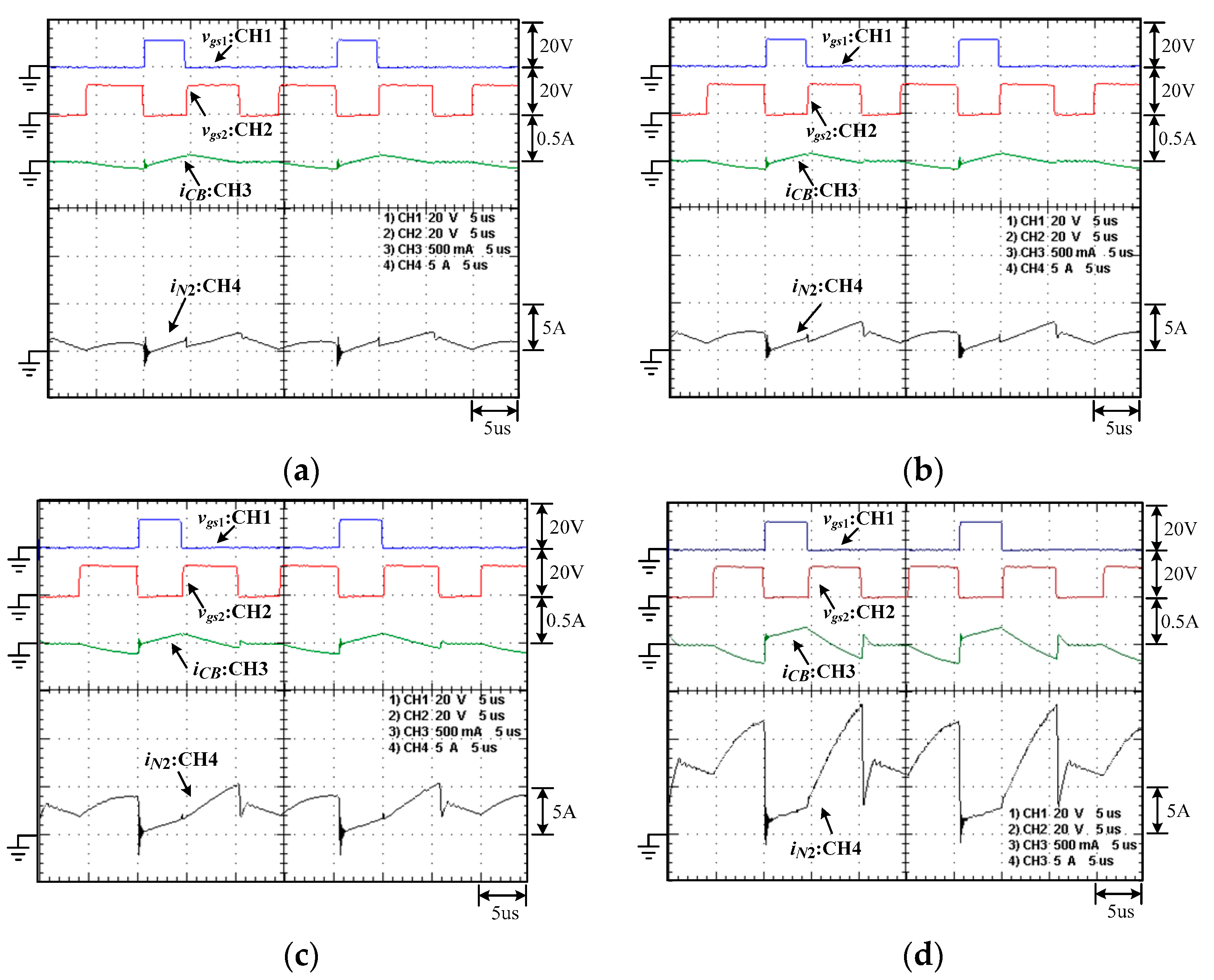
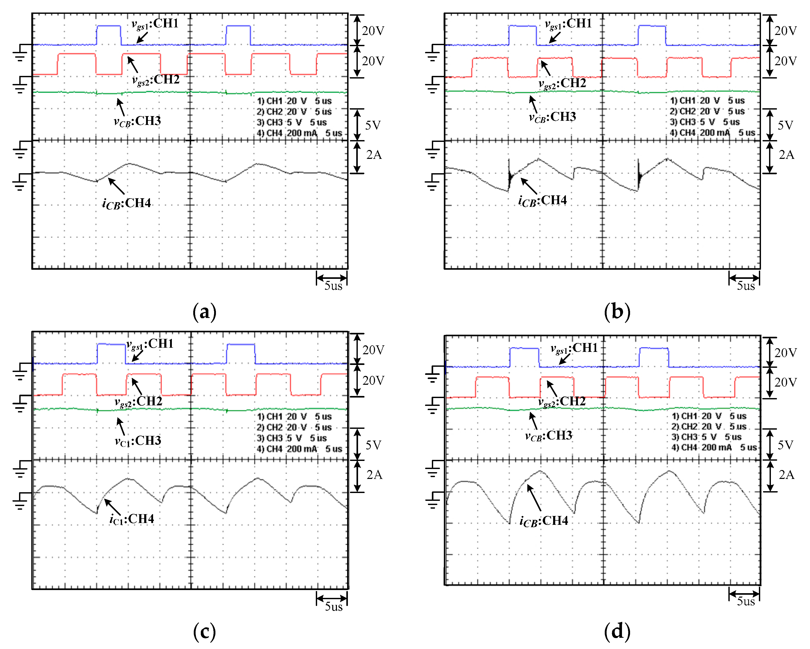
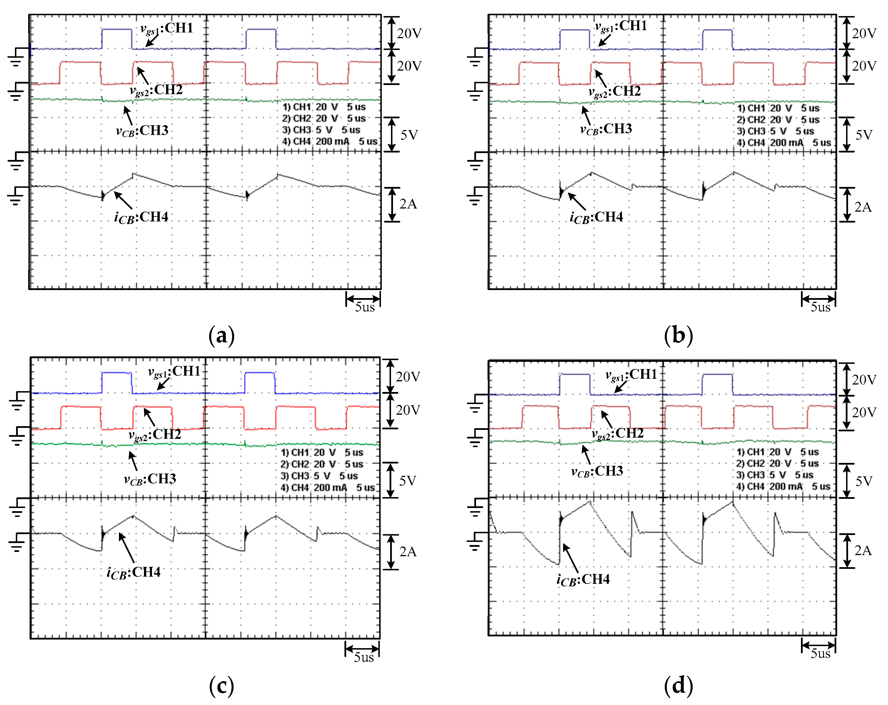
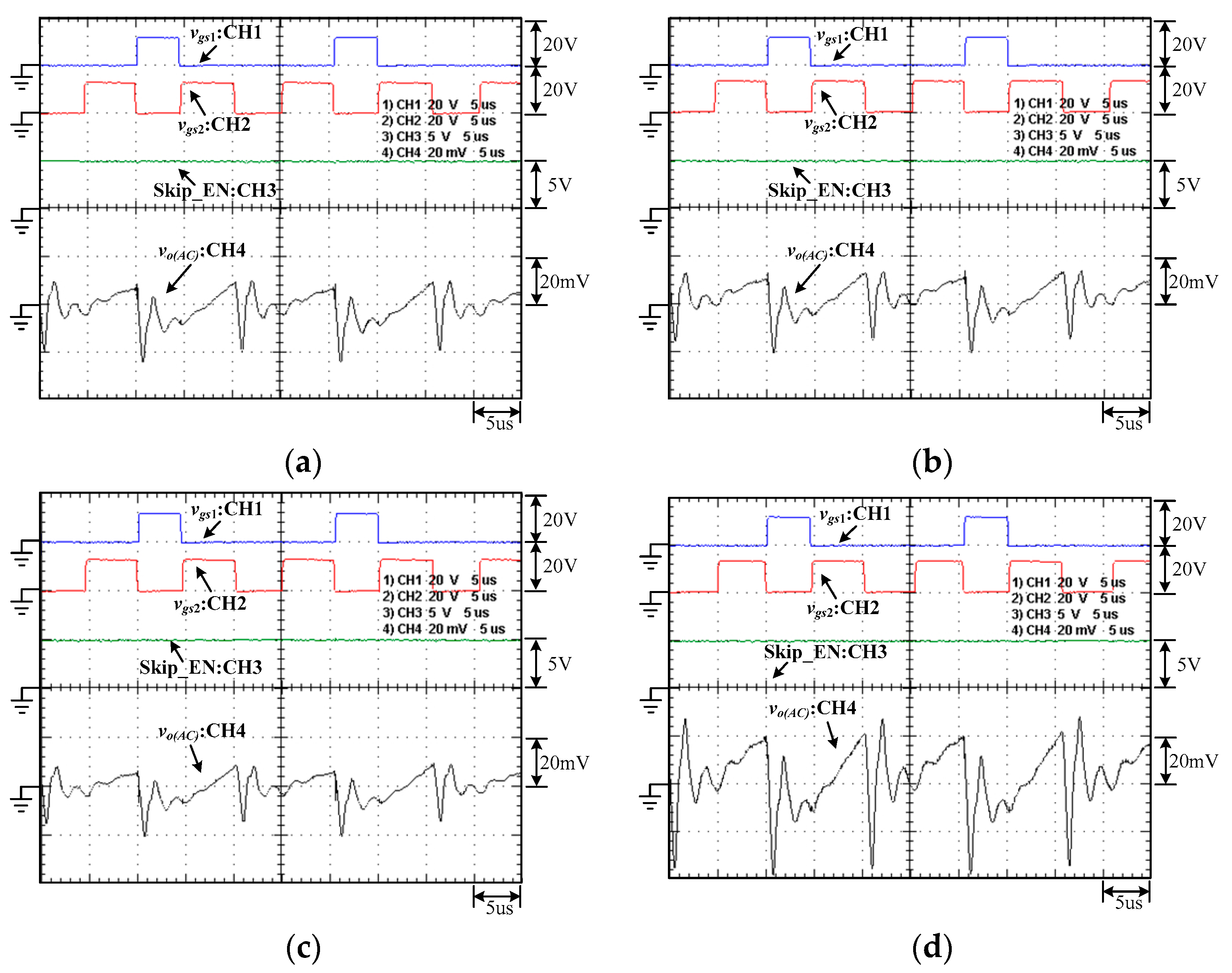
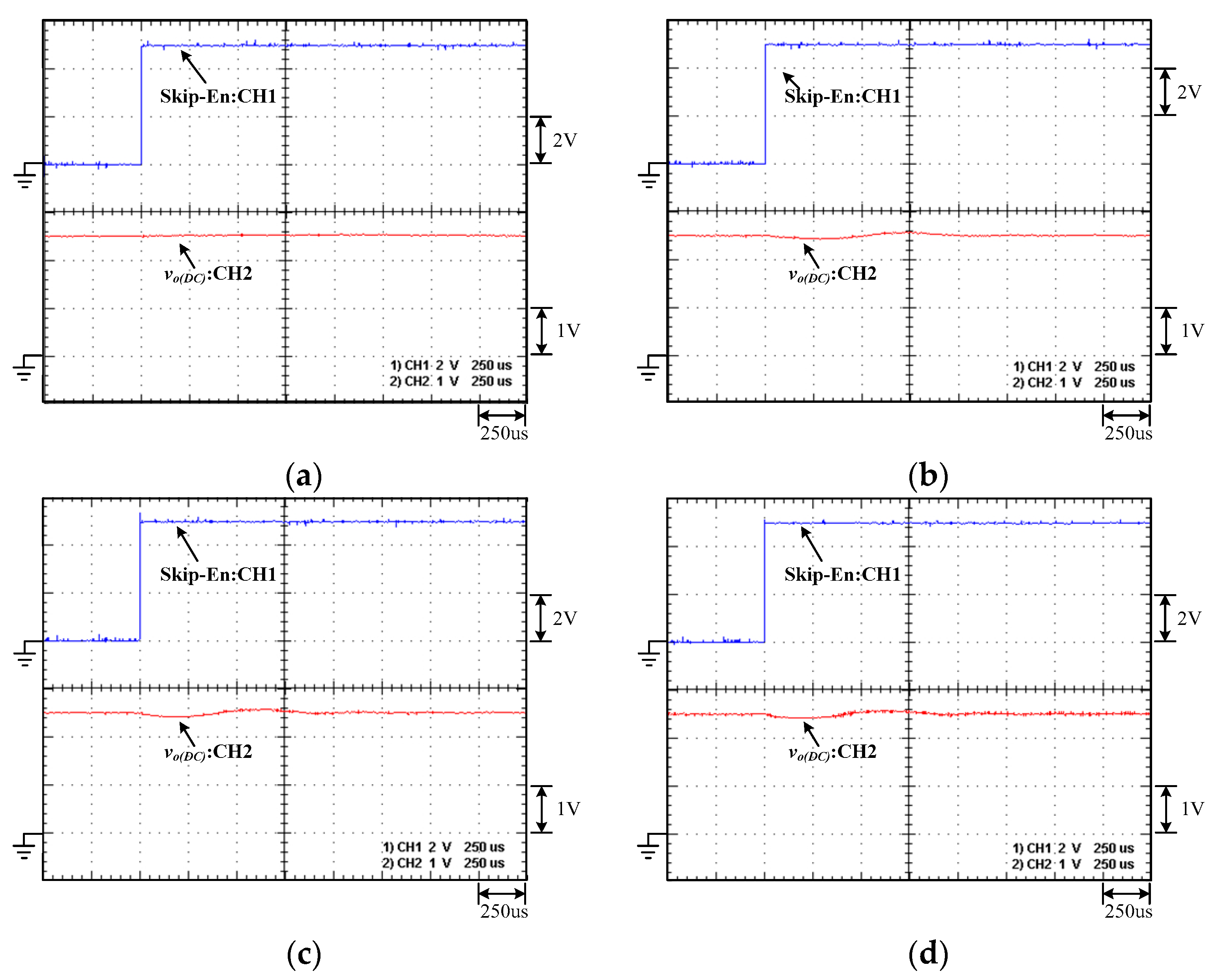
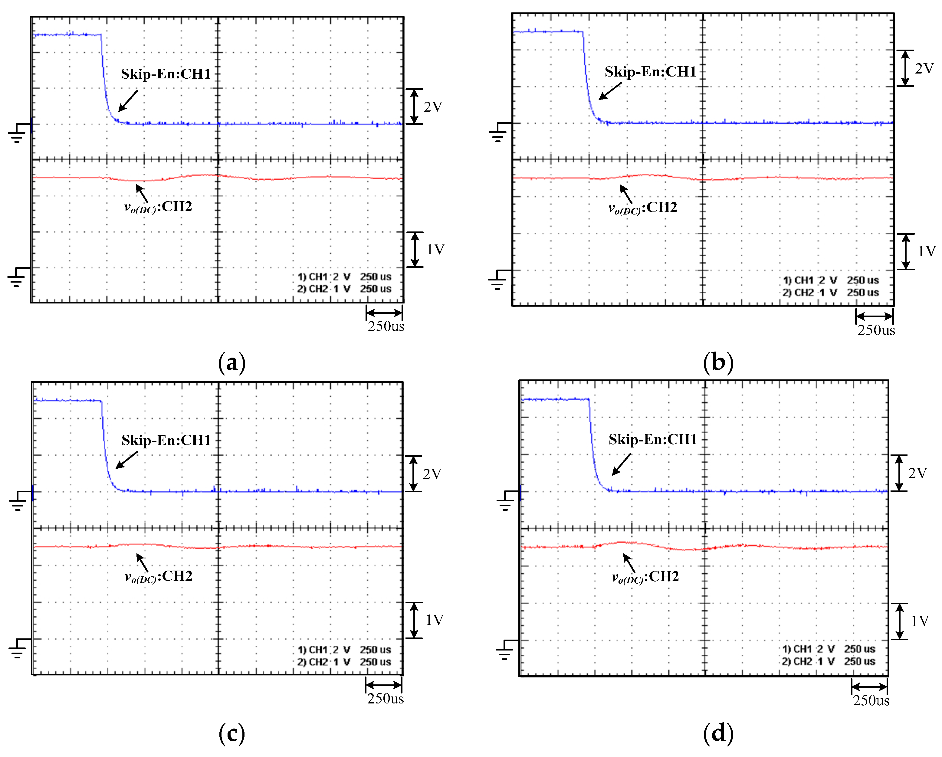
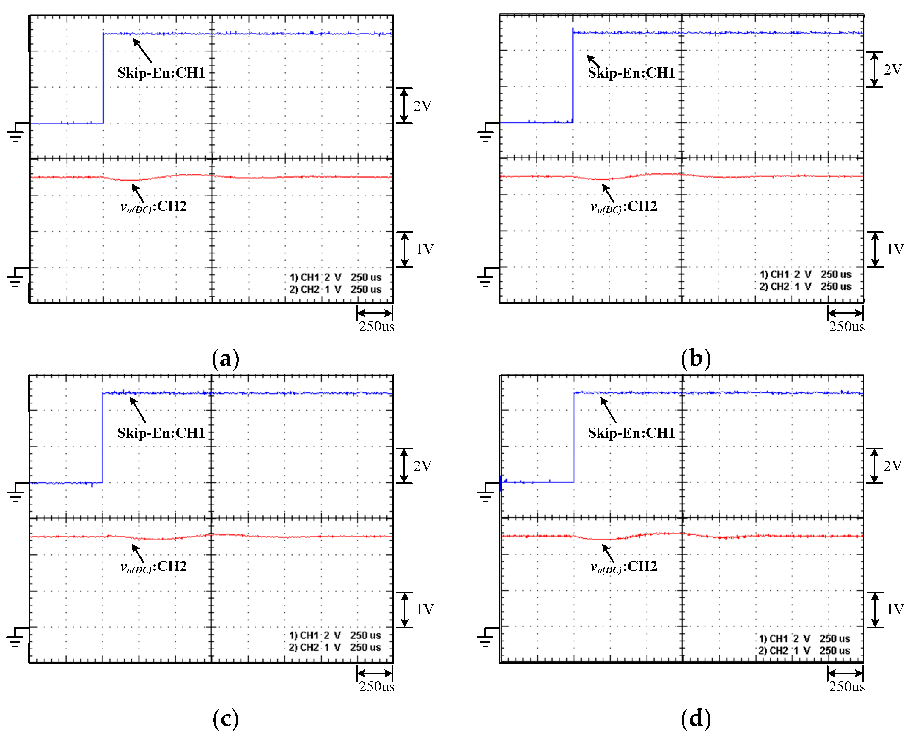
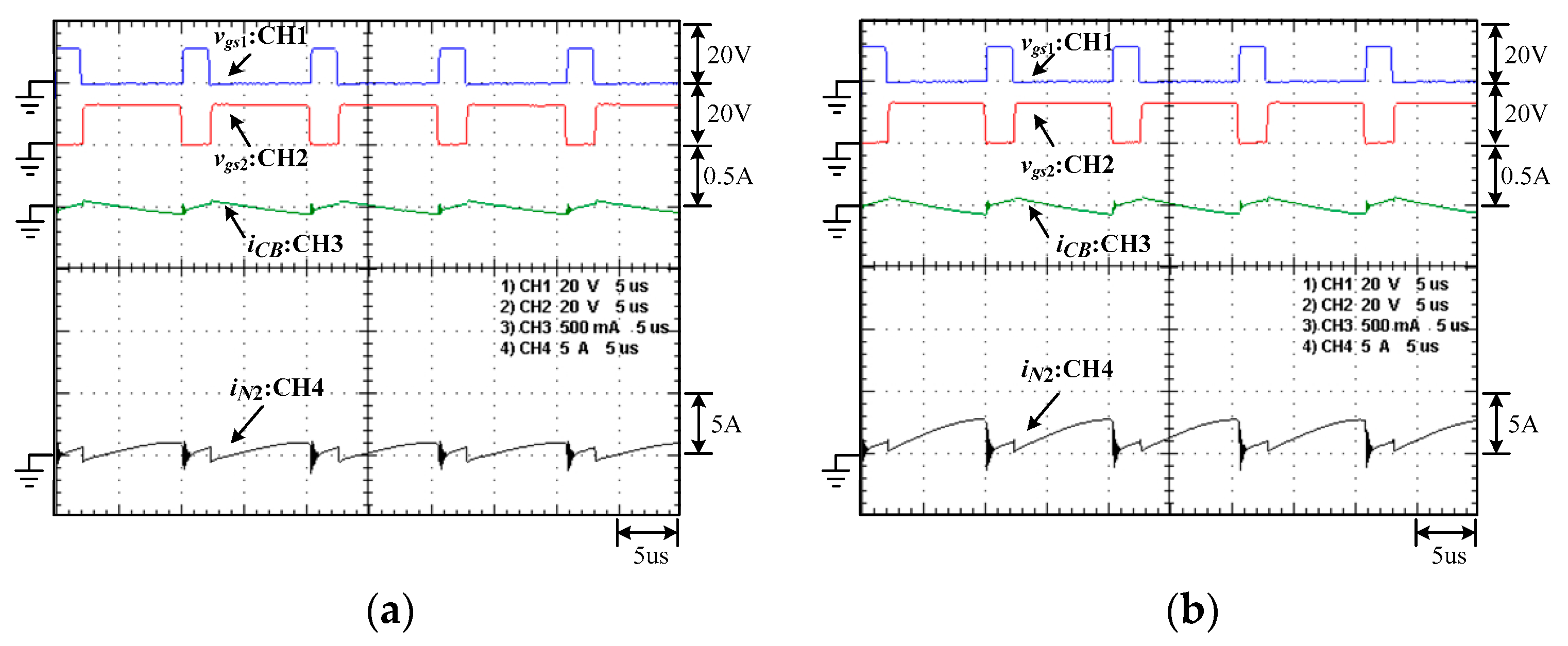
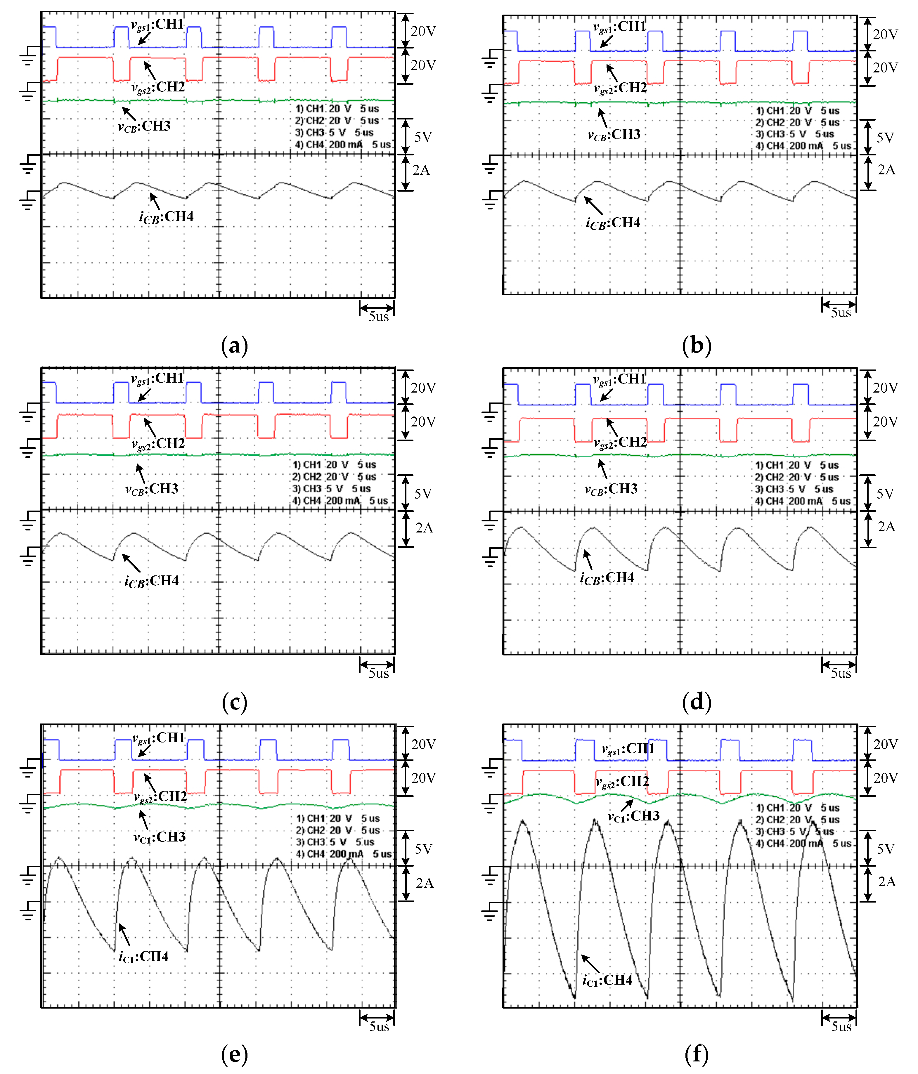
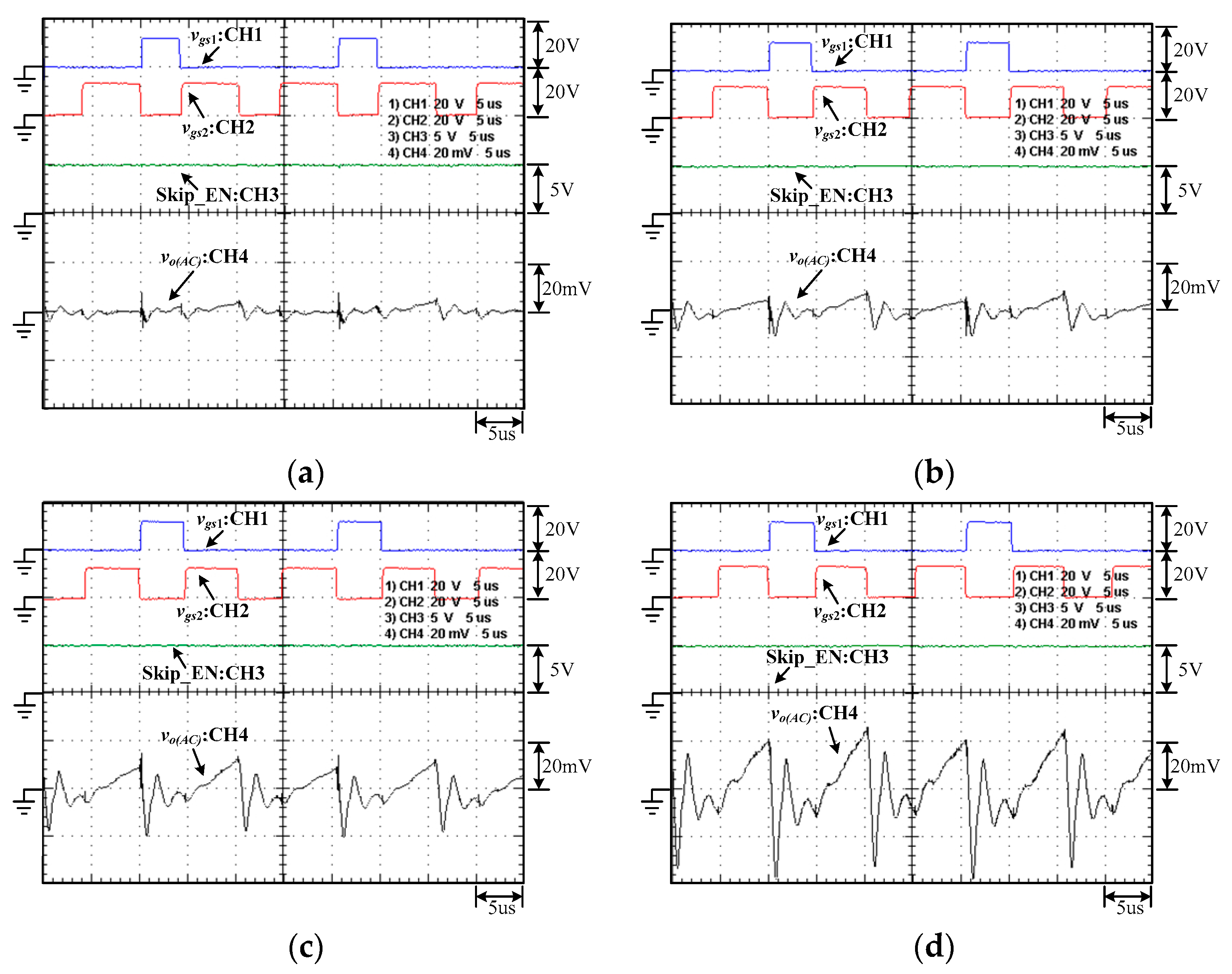
4. Experimental Results
5. Discussion
6. Conclusions
Author Contributions
Funding
Data Availability Statement
Conflicts of Interest
Abbreviations
| AC | Alternating Current |
| CCM | Continuous Current Mode |
| DC | Direct Current |
| IC | Integrated Circuit |
| POL | Power on Load |
| PWM | Pulse-Width-Modulated |
| ZVS | Zero Voltage Switching |
References
- Ren, Y.; Xu, M.; Yao, K.; Meng, Y.; Lee, F.C.; Guo, J. Two-stage approach for 12 V VR. In Proceedings of the Nineteenth Annual IEEE Applied Power Electronics Conference and Exposition (APEC '04), Anaheim, CA, USA, 22–26 February 2004; pp. 1306–1312. [Google Scholar]
- Ren, Y.; Xu, M.; Yao, K.; Lee, F.C. Two-stage 48V power pod exploration for 64-bit microprocessor. In Proceedings of the Eighteenth Annual IEEE Applied Power Electronics Conference and Exposition (APEC '03), Miami Beach, FL, USA, 9–13 February 2003; pp. 426–431. [Google Scholar]
- Ren, Y.; Xu, M.; Yao, K.; Lee, F.C. 12V VR efficiency improvement based on two-stage approach and a novel gate driver. In Proceedings of the 2005 IEEE 36th Power Electronics Specialists Conference, Recife, Brazil, 16 June 2005; pp. 2635–2641. [Google Scholar]
- Mao, H.; Abu-Qahouq, J.A.; Luo, S.; Batarseh, I. Zero-voltage-switching (ZVS) two-stage approaches with output current sharing for 48 V input DC-DC converter. In Proceedings of the Nineteenth Annual IEEE Applied Power Electronics Conference and Exposition (APEC '04), Anaheim, CA, USA, 22–26 February 2004; Volume 2, pp. 1078–1082. [Google Scholar]
- Hwu, K.I.; Yau, Y.T. Resonant voltage divider with bidirectional operation and startup considered. IEEE Trans. Power Electron. 2012, 27, 1996–2006. [Google Scholar] [CrossRef]
- Li, W.; Xiao, J.; Wu, J.; Liu, J.; He, X. Application summarization of coupled Inductors in DC-DC converters. In Proceedings of the 2009 Twenty-Fourth Annual IEEE Applied Power Electronics Conference and Exposition, Washington, DC, USA, 15–19 February 2009; pp. 1487–1492. [Google Scholar]
- Li, W.; He, X. A family of interleaved DC-DC converters deduced from a basic cell with winding-cross-coupled inductors (WCCIs) for high step-up or step-down conversions. IEEE Trans. Power Electron. 2008, 23, 1791–1801. [Google Scholar] [CrossRef]
- Lee, I.; Cho, S.; Moon, G. Interleaved buck converter having low switching losses and improved step-down conversion ratio. IEEE Trans. Power Electron. 2012, 27, 3664–3675. [Google Scholar] [CrossRef]
- Tsai, C.; Shen, C. Interleaved soft-switching buck converter with coupled inductors. In Proceedings of the 2008 IEEE International Conference on Sustainable Energy Technologies, Singapore, 24–27 November 2008; pp. 877–882. [Google Scholar]
- Zhang, Z.; Meyer, E.; Liu, Y.; Sen, P.C. A non-isolated ZVS self-driven current tripler topology for low voltage and high current applications. In Proceedings of the 2009 IEEE Energy Conversion Congress and Exposition, San Jose, CA, USA, 20–24 September 2009; pp. 1983–1990. [Google Scholar]
- Jang, Y.; Jovanovic, M.M.; Panov, Y. Multiphase buck converters with extended duty cycle. In Proceedings of the Twenty-First Annual IEEE Applied Power Electronics Conference and Exposition (APEC '06), Dallas, TX, USA, 19–23 March 2006; pp. 8–44. [Google Scholar]
- Grant, D.A.; Darroman, Y.; Suter, J. Synthesis of tapped-inductor switched-mode converters. IEEE Trans. Power Electron. 2007, 22, 1964–1969. [Google Scholar] [CrossRef]
- Ye, S.; Eberle, W.; Liu, Y. A novel non-isolated full bridge topology for VRM applications. IEEE Trans. Power Electron. 2008, 23, 427–437. [Google Scholar] [CrossRef]
- Cheng, H.; Smedley, K.M.; Abramovitz, A. A wide-input–wide-output (WIWO) DC–DC converter. IEEE Trans. Power Electron. 2010, 25, 280–289. [Google Scholar] [CrossRef]
- Batarseh, M.; Wang, X.; Batarseh, I. Non-isolated half bridge buck based converter for VRM application. In Proceedings of the 2007 IEEE Power Electronics Specialists Conference, Orlando, FL, USA, 17–21 June 2007; pp. 2393–2398. [Google Scholar]
- Nishijima, K.; Ishida, D.; Harada, K.; Nabeshima, T.; Sato, T.; Nakano, T. A novel two-phase buck converter with two cores and four windings. In Proceedings of the INTELEC 07 - 29th International Telecommunications Energy Conference, 30 September–4 October 2007; pp. 861–866. [Google Scholar]
- Yao, K.; Ren, Y.; Wei, J.; Xu, M.; Lee, F.C. A family of buck-type DC-DC converters with autotransformers. In Proceedings of the Eighteenth Annual IEEE Applied Power Electronics Conference and Exposition (APEC '03), Miami Beach, FL, USA, 9–13 February 2003; pp. 114–120. [Google Scholar]
- Yang, Z.; Ye, S.; Liu, Y. A new transformer-based non-isolated topology optimized for VRM application. In Proceedings of the 2005 IEEE 36th Power Electronics Specialists Conference, Recife, Brazil, 16 June 2005; pp. 447–453. [Google Scholar]
- Vafaie, M.H.; Adib, E.; Farzanehfard, H. A self powered gate drive circuit for tapped inductor buck converter. In Proceedings of the 2012 3rd Power Electronics and Drive Systems Technology (PEDSTC), Tehran, Iran, 15–16 February 2012; pp. 379–384. [Google Scholar]
- Hwu, K.I.; Jiang, W.; Yau, Y.T. Ultra high step-down converter. IEEE Trans. Power Electron. 2015, 30, 3262–3274. [Google Scholar] [CrossRef]
- Yau, Y.T.; Jiang, W.Z.; Hwu, K.I. Analysis and design of a high-step-down ratio resonant converter. Power Electron. 2016, 9, 864–873. [Google Scholar] [CrossRef]


| Input voltage Vin | 48 V |
| Output voltage Vo | 2.5 V |
| Output rated current Io | 20 A |
| Switching frequency fs | 100 kHz |
| Capacitor CB | 20 uF/50 V TDK MLCC |
| Coupled inductor | N1:N2 = 24:8 with Lm = 87.1 uH, LLK1 = 3.94 uH, and LLK2 = 0.69 uH MPP core of Micrometals Co. (Colorado Springs, CO, USA), model T106-M125 |
| Capacitor Co | 2 × 1000 uF solid electrolytic capacitor |
| , | AON6244, withstand voltage 60 V, 4.7 mΩ, Alpha and Omega Co. (Sunnyvale, CA, USA) |
| AON6512, withstand voltage 30 V, 1.7 mΩ, Alpha and Omega Co. |
Publisher’s Note: MDPI stays neutral with regard to jurisdictional claims in published maps and institutional affiliations. |
© 2021 by the authors. Licensee MDPI, Basel, Switzerland. This article is an open access article distributed under the terms and conditions of the Creative Commons Attribution (CC BY) license (http://creativecommons.org/licenses/by/4.0/).
Share and Cite
Yau, Y.-T.; Wang, C.-W.; Hwu, K.-I. Light-Load Efficiency Improvement for Ultrahigh Step-Down Converter Based on Skip Mode. Electronics 2021, 10, 355. https://doi.org/10.3390/electronics10030355
Yau Y-T, Wang C-W, Hwu K-I. Light-Load Efficiency Improvement for Ultrahigh Step-Down Converter Based on Skip Mode. Electronics. 2021; 10(3):355. https://doi.org/10.3390/electronics10030355
Chicago/Turabian StyleYau, Yeu-Torng, Chao-Wei Wang, and Kuo-Ing Hwu. 2021. "Light-Load Efficiency Improvement for Ultrahigh Step-Down Converter Based on Skip Mode" Electronics 10, no. 3: 355. https://doi.org/10.3390/electronics10030355
APA StyleYau, Y.-T., Wang, C.-W., & Hwu, K.-I. (2021). Light-Load Efficiency Improvement for Ultrahigh Step-Down Converter Based on Skip Mode. Electronics, 10(3), 355. https://doi.org/10.3390/electronics10030355