Abstract
The significant rise in the cost of manufacturing nanoscale integrated circuits (ICs) has led the majority of IC design companies to outsource the fabrication of their products to other companies, often located in different countries. The multinational nature of the hardware supply chain has led to a host of security threats, including IP piracy, IC overproduction, and Trojan insertion. To combat these, researchers have proposed logic locking techniques to protect the intellectual properties of the design and increase the difficulty of malicious modification of its functionality. However, the adoption of logic locking approaches has been rather slow due to the lack of integration with the IC production process and the lack of efficacy of existing algorithms. This work automates the logic locking process by developing software using Python that performs the locking on a gate-level netlist, which can be integrated with the existing digital synthesis tools. Analysis of the latest logic locking algorithms has demonstrated that the SFLL-HD algorithm is one of the most secure and versatile when trading-off levels of protection against different types of attacks and was thus selected for implementation. The presented tool can also be expanded to incorporate the latest locking mechanisms to keep up with the fast-paced development in this field. The paper also presents a case study to demonstrate the functionality of the tool and how it could be used to explore the design space and compare different locking solutions.
1. Introduction
The production of nanoscale integrated circuits (ICs) has become a multinational distributed process; a trend driven by the increase in the level of outsourcing to reduce costs. This has led to a significant increase in security risks. This is because of the larger number of entities and organizations that have become part of this process, which has made it easier for adversaries to infiltrate the hardware supply chain, steal design secrets, or maliciously modify its functionality.
Typical countermeasures include passive hardware metering and IP watermarking that are capable of detecting IP piracy and overproduction. Other emerging approaches include active hardware metering and logic locking, which are capable of preventing these risks. Logic locking techniques insert a locking mechanism and new key inputs to the design, such that when a circuit is locked it manifests incorrect behavior until the right key combination is applied. There are two categories of logic locking: combinational and sequential. Combinational [1] logic locking corrupts the outputs of the circuit unless the correct key is applied, while sequential [2] logic locking inserts additional states, meaning that the state of the circuit will only become functional upon application of the correct sequence, otherwise it remains in a non-functional state, i.e., “locked”.
All ICs locked with a combinational logic locking algorithm can have the same key (global key) or every IC can be locked by a unique key (individual key). In the latter case, the key which is applied to the IC (chip key) is fed to the key preprocessor to derive the internal key that unlocks the circuit. The uniqueness of the chip key is achieved with physically unclonable function (PUF) technology. In a logic locking scheme that uses a global key, the chip key is equal to the internal key and is the same for every IC. [3]. Random logic locking [1] was the first logic locking technique introduced. It randomly inserts XOR/XNOR gates in the gate-level netlist to obfuscate the outputs. It is broken by sensitization attacks [4] along with fault-based logic locking [5], which is a technique that improves the obfuscation of the outputs. Strong logic locking [4] is designed to be resilient to sensitization attacks but can be broken by an SAT attack [6], which uses SAT solvers to break the logic locking algorithms. Cyclic logic locking [7] thwarts an SAT attack by creating logical loops in the circuit but it can be broken by a modified SAT attack—CycSAT [8]. Anti-SAT [9] and SARLock [10] are algorithms designed to thwart SAT attacks by adding external logic, which makes SAT attacks exponentially dependent on the number of possible key combinations. However, those two algorithms both have low corruptibility and are broken by removal attacks [11,12]. Tenacious and traceless logic locking (TTL) [13] and its enhancement, stripped functionality logic locking—Hamming distance (SFLL-HD) [14], are resilient to both SAT and removal attacks and SFLL-HD provides a solid level of corruptibility. Along with these algorithms, which lock a design on a gate-level, some algorithms lock a design on the RTL level such as SFLL-HLS [15] and ASSURE [16].
These concerted efforts to develop more secure logic locking mechanisms have so far not led to the wide adoption of this approach. This is partly due to the lack of integration of these techniques with the IC design process. There have been few investigations that aimed at addressing this issue. For example, the authors of [17] present an approach to scale up a logic locking scheme to a multi-module design, however, the authors have not presented an automation tool for their proposed framework that allows the reproducibility of the work.
Therefore, this work aims to develop a framework to incorporate logic locking in the standard digital design flow. To achieve this, this paper first systematically reviews existing algorithms to identify the best candidate to adopt and subsequently develops a software tool to automate the locking process and allow integration with the current IC design flow. The proposed tool can be used by IP developers to protect their designs from piracy. The software can also be easily extended to include other logic locking algorithms. The main contributions of this work are as follows:
- (1)
- It provides a comprehensive comparison of the state-of-the-art logic locking methods.
- (2)
- It develops a proof-of-concept logic locking automation tool compatible with the standard IC design process. The software is demonstrated to successfully obfuscate a gate-level netlist by locking one of its input cones using the SFLL-HD algorithm. The correct functionality of the tool was demonstrated in simulation and the tool succeeds in providing the same obfuscation level as in the algorithm specification.
- (3)
- It provides rigorous analysis of the tool’s performance and the overheads of the resulting netlist in terms of area, power usage, and critical path delay.
The remainder of this paper is structured as follows. Section 2 discusses the threat model and reviews the state-of-the-art logic locking algorithms and related attacks. Section 3 presents the design and implementation of the logic locking tool. Section 4 provides experimental verification of the functionality of the developed tool, and demonstrates, through several case studies, how it can be used to explore the design space. Conclusions and future work are presented in Section 5.
2. A Review of Logic Locking Algorithms and Related Attacks
Logic locking algorithms have been developed in response to emerging threats against the hardware supply chain, in particular, these techniques can be used to mitigate the risks of IP piracy through reverse engineering, IC overproduction, and Trojan insertion. The essence of this approach is to modify the design by adding a locking mechanism, making it harder for an adversary to steal design secrets, create unauthorized copies of fabricated chips, or perform a meaningful modification for the netlist to insert a Trojan. This section reviews existing logic locking algorithms and related attacks.
It is worth pointing out that this work only considers techniques associated with oracle-guided attacks. However, algorithms associated with the oracle-less attacks [18,19] can also be incorporated into the proposed framework.
2.1. Principles of Random Logic Locking
This approach is based on the insertion of XOR and XNOR key gates at signal lines chosen randomly [1]. The key values of these gates are “0” and “1” respectively. An inverter can be added at the same signal line which flips the key value. The idea of this approach is to prevent the adversary from guessing the key value based on the gate type since the adversary does not know whether the aforementioned inverter is part of the original circuit or is added in the process of logic locking. Upon application of the wrong key bit, the appropriate signal is flipped and propagated to the output. This makes the output obfuscated. Random logic locking is susceptible to sensitization attacks [4] as shown below.
2.2. Sensitization Attacks on Random Logic Locking
The sensitization attack [4] aims to obtain the key bits by applying specific input patterns to sensitize the key inputs to output without it being masked. To successfully perform this attack, the attacker has to have the obfuscated netlist as well as an unlocked IC, which can be obtained from the market. The adversary can then distinguish several types of key gates based on their locations and interference with other key gates, as listed below.
- Isolated key gates—a key gate without a path to and from any other key gate. A key value of an isolated key gate can be propagated to the output by applying an appropriate input pattern on the unlocked IC.
- Runs of key gates—a set of key gates connected one to another (in a run). A run of key gates can be replaced by only one key gate.
- Dominating key gates—a dominating key gate lies on every path between another key gate and outputs. To determine the value of the dominating key gate, the attacker has to find an input pattern that sensitizes its value to the output and prevents the key value of a dominated key gate from being propagated.
- Concurrently mutable convergent key gates—two gates without a path between one another that converge at the third gate. Key values of both gates can be sensitized to output by muting the effect of the other key gate and the attacker has to find an input pattern that enables this situation.
- Sequentially mutable convergent key gates—two gates without a path between one another that converge at the third gate. The only key value of one gate can be sensitized to output by muting the effect of the other gate, while the reciprocal situation is not possible. The attacker finds the input pattern that unveils the key value of the first gate and replaces it with an inverter or a buffer depending on the determined key value before targeting the other key gate.
- Non-mutable convergent key gates—two gates without a path between one another that converge at the third gate and none of them can be muted to sensitize the other one’s value to the output. In this case, the attacker has to perform a brute force attack.
2.3. Principles of Fault Analysis-Based Logic Locking
The goal of fault-based logic locking [5] is to achieve a 50% Hamming distance between correct and obfuscated outputs. This is realized by inserting key gates at locations with the highest fault impact, i.e., the ability to affect most of the outputs if a fault occurs at that location. Fault impact is calculated for every possible key gate location based on the number of patterns that detect the stuck-at-0 (NoP0) or stuck-at-1 (NoP1) fault and the number of outputs that are affected by that fault (NoO0 and NoO1).
The XOR/XNOR key gate is inserted at the location with the highest fault impact, the netlist is updated and the process repeats as many times as the size of the key. The circuit can be additionally obfuscated by replacing the key gate type and inserting an inverter at its output. While fault-based logic locking provides better obfuscation than random logic locking, it is still susceptible to sensitization attacks.
2.4. Principles of Strong Logic Locking
Strong logic locking [4] is an algorithm designed to be resilient to sensitization attacks. This is achieved by inserting key gates in such a manner that there is interference between multiple key gates, i.e., sensitization of most of the key inputs is possible only with knowledge of another key input. After the initial 10% of the key gates are inserted randomly, every other key gate is being inserted such that the interference with previously inserted key gates is maximized. Metric for this is calculated by assigning every type of interference a unique weight and summing all weights for the previously inserted key gates (isolated gates have the lowest weight, mutable gates with existing golden pattern have higher weight, while mutable gates without a golden pattern and non-mutable gates have the highest weight). This is performed for each possible key gate location, after which the location with the highest cumulative weight is selected and the netlist is updated. However, strong logic locking can be broken by an SAT attack [6].
2.5. SAT Attacks on Random Logic Locking
An SAT attack [6] uses SAT solvers to derive Boolean expressions from a locked circuit and successively eliminate incorrect keys for distinguishing input patterns until the correct key is found. The attacker has to have an obfuscated netlist and an unlocked IC which can be used as a black box. An SAT solver forms an expression that will be satisfied for an input pattern that yields different outputs for different keys. Those patterns are called distinguishing input patterns. This input pattern is then applied to an unlocked IC and keys that yield incorrect outputs are ruled out. The algorithm continues to find distinguishing input patterns and eliminate incorrect keys until the correct key is found.
2.6. Principles of Cyclic Logic Locking
Cyclic logic locking [7] thwarts an SAT attack by creating logical loops in the circuit. There are two types of loops in the circuit flow graph: reducible and non-reducible. All loops created by the cyclic logic locking algorithm have to be non-reducible. This means that the loop cannot be uniquely traversed by depth-first search and the created edge cannot be identified. Another goal of the algorithm is to have at least n ≥ 2 removable edges which results in a loop complexity of 2n. A removable edge can be removed from the graph by modifying the key-value and whose removal would not leave any gate without any input or output. In practice, these loops are realized with multiplexers. Key inputs are used as select inputs of multiplexers, where the correct key value selects the normal path, while the incorrect key value selects a path with a loop. An SAT attack is thwarted because an SAT solver gets stuck in an infinite loop. After all, it cannot represent the circuit in a form of a directed acyclic graph. However, the modified CycSAT [8] attack algorithm, which has a preprocessing step for detection and avoidance of cycles, breaks the cyclic logic locking algorithm.
2.7. Principles of Anti-SAT
Anti-SAT [9] is an SAT resilient technique. It locks the circuit by using two complementary functions whose inputs are the key gate outputs. Inputs of the key gates are key inputs and a set of signals from the circuit. Each signal from the set is fed to exactly two key gates, such that the output of one is fed to one function block, while the other is fed to the complementary function block. Outputs of both function blocks are fed to an AND gate and are used to invert a particular output. An SAT attack is thwarted by making the number of iterations needed for the elimination of all incorrect keys exponentially dependent on the number of bits used for the key. However, Anti-SAT has low corruptibility of outputs since it only locks the circuit for specific input combinations and is therefore often used in combination with another logic locking technique, such as SLL. Apart from low corruptibility, it is also susceptible to removal attacks [11], which unveil the original circuit.
2.8. Principles of SARLock
SARLock [10] is an SAT resilient technique. It locks the circuit by adding the external logic which inverts the desired output of the circuit for exactly one input pattern per key combination and restores that inversion for the correct key. This thwarts an SAT attack because the attack algorithm can eliminate only one incorrect key per iteration, which makes the complexity of the algorithm exponentially dependent on the number of bits used for the key. Similar to Anti-SAT, SARLock also has low corruptibility and has to be used in combination with another logic locking technique, and is susceptible to a removal attack [12].
2.9. Removal Attacks on SAT Resilient Techniques
A removal attack [11,12] is the main threat to logic locking algorithms such as Anti-SAT and SARLock, which have the locking circuitry decoupled from the original circuit. To perform this attack, the attacker only has to have an obfuscated netlist. The greatest vulnerability of the Anti-SAT block is that it is connected to the rest of the netlist with only one signal Y, the one that inverts a particular output. If that signal is identified, its input logic cone can be removed and the circuit can be re-synthesized using the correct value of the signal Y. The identification of the signal Y is performed by identifying its inputs, two complementary functions, using the signal probability skew (SPS) attack [11,12]. These functions are designed to have a high probability skew towards 1 and 0 to achieve resilience to SAT attacks.
SARLock is also vulnerable to signal probability skew attacks. Comparator logic in the SARLock structure is comprised of an AND tree and can be easily identified by the SPS attack. The SARLock protection structure can then be removed and the original circuit is restored.
2.10. Inter-Module SAT Techniques
In [20], an HW/SW secure solution is proposed where the inter-lock framework is used as a logic locking algorithm and a 1024-bit key is applied to the locked circuit. To achieve higher compatibility, the solution adopts open-source ISA RISC-V for hardware. The microkernel seL4 is used as an operating system for the protected IC. As the system is simpler than a monolithic kernel (e.g., Linux) a lesser security threat is generated. The authors of [21] argue that different modules on an IC product should not be locked in isolation, hence they propose an inter-lock framework wherein modules are not just locked by keys stored in tamper-proof memory, but also generated by other modules, hence effectively increasing key length without increasing tamper-proof memory. As locking keys are not only output from tamper-proof memory, it is hard for the attacker to find the position of all key bits. However, more advanced hardware Trojans can be inserted into the circuit without fully understanding its functionality. In this case, inter-connection signals between modules are considered as vulnerable points of the design. The authors of [22] presented a control lock, which is a key-dependent logic locking framework that assures the inter-module signals are distorted even when the correct key is applied, hence protecting the circuit from the advanced Trojan insertion
2.11. Principles of Tenacious and Traceless Logic Locking
Tenacious and traceless logic locking (TTL) [13] inverts the output of a logic cone for one protected input pattern by modifying the cone via logic gate insertions or replacements. Modified logic cones now have inverted outputs only for the protected input pattern. The functionality is restored by a restored unit. Upon applying the correct key, logic fixes are restored in this inversion by a flip signal. For incorrect keys, the restoring unit adds inversion for all other input patterns except the protected input pattern, because the logic cone was modified such that those patterns were not inverted. TTL is resilient to removal attacks because identifying the skewed flip signal and removing the protection logic would recover only the modified logic cone and not the original circuit. TTL has low corruptibility since for all incorrect keys the output is inverted for only one input pattern. An SAT attack can thus eliminate only one incorrect key per iteration and is unfeasible due to its exponential complexity. Resilience to an SAT attack is achieved by ensuring that an SAT attack always encounters its worst-case scenario. DIP can eliminate only one incorrect key per iteration requiring 2k−1 iterations for finding the correct key, considering k as the bit width of the key. Since the SAT attack chooses the key randomly, it can guess the correct key with the probability of for a single iteration. For a key with sufficiently large bit widths, it is infeasible to perform an SAT attack because of the exponential complexity.
2.12. Principles of Stripped Functionality Logic Locking—Hamming Distance
Stripped functionality logic locking with Hamming distance (SFLL-HD) [14] is a technique similar to TTL. Similar to most other logic locking techniques, SFLL-HD focuses on the defense of an oracle-guided attack. Instead of having only one protected input pattern of a logic cone, it protects all input patterns that are a Hamming distance h from a protected pattern. A functionality stripped circuit is a modified logic cone such that the output of the cone is inverted for all input patterns that are a Hamming distance h from a protected pattern. A restore unit compares the input pattern with the applied key and inverts the functionality-stripped output if the Hamming distance from the applied key and input pattern is h. If the applied key is correct, this inversion restores the inversion made in the functionality tripped circuit. When h equals zero, SFLL-HD has the same behavior as TTL. However, for h different from zero, SFLL-HD has different corruptibility and resilience to SAT and removal attacks, so its performance is configurable with h. A Hamming distance closer to k/2 provides better corruptibility, but there is a trade-off between corruptibility and resilience to SAT and removal attacks. The number of protected input patterns is so for h closer to k/2 the corruptibility is highest. However, this increased number of protected input patterns makes the probability of an SAT attack to randomly guess the key that can eliminate all incorrect keys at once equal to . For h equal to k/2, that probability is highest and is equal to . For h equal to k/2, that probability is highest and is equal to . For k = 32 and h = 16, that probability is close to 14% compared to the case when k = 32 and h = 0 when that probability is , same as in TTL. Resilience to removal attacks is also dependant on the number of protected input patterns. The resilience to removal attacks gets linearly higher with a larger number of protected input patterns [14]. By changing the Hamming distance parameter, h, one can configure corruptibility and resilience to SAT and removal attacks concerning TTL. The work in [23] suggests that high resilience and high output corruption of logic locking can be achieved at the same time, however, higher overhead has to be tolerated for this. Values of h closer to 0 or key size k make the algorithm more resilient to SAT attacks, while values closer to k/2 provide better resilience to removal attacks.
2.13. Analysis of Algorithms
The decision on which an algorithm should be implemented was made after the analysis that focused on the corruptibility of the outputs and resilience on different attacks.
As we can see from Table 1, different algorithms provide different levels of security against the aforementioned attacks. Most primitive logic locking techniques, random logic locking, and fault-based logic locking, despite providing high corruptibility are susceptible to sensitization attacks and are not suitable for implementation. SLL is also not suitable for implementation because, even though it is designed to be resilient to sensitization attacks, it is susceptible to SAT attacks. Some SAT resilient techniques such as Anti-SAT and SARLock are susceptible to removal attacks, while TTL is resilient to all three attacks but provides low corruptibility. Cyclic logic locking, on the other hand, is resilient to all three attacks and provides high corruptibility, but is broken by a modified SAT attack (CycSAT) and will thus not be implemented. SFLL-HD is resilient to sensitization attacks and resilience to SAT attacks, removal attacks, and corruptibility can be traded-off by choice of Hamming distance h. Even though there have been successful attempts to unlock circuits locked with the SFLL-HD algorithm [24,25,26], so far it has remained the most secure logic locking algorithm and is therefore chosen to be implemented.

Table 1.
Comparison of logic locking algorithms.
2.14. Analysis of Strategies
In pre-SAT logic locking strategies (RLL, FLL, SLL) locking gates were inserted separately all around the entire designed circuit. Locking gates inserted in this fashion are hard to be detected or removed. However, to protect the design against SAT attacks, locking techniques such as SARLock and Anti-SAT introduce extra blocks to the circuit to reduce the number of the wrong key that each input pattern can eliminate. Compared with using a simple (one XOR gate) and distributed locking gate, introducing an extra block, although providing high SAT attack resilience, makes the design vulnerable to removal attacks. TTL combine the two strategies, achieving satisfying resilience to SAT and removal attacks at the same time. However, to achieve low DIP efficiency, TTL ends up with low output corruptibility, hence low resilience to approximate attacks. SFLL-HD on the other hand, allows the designer to adjust the number of each input pattern they can eliminate, by which the locked circuit can achieve high output corruption while maintaining a relatively high SAT resilience.
3. Automation of Logic Locking
3.1. Internal Structure of the Tool
The tool developed for automation of SFLL-HD can be decomposed into three clusters:
- Parsing the input netlist and transforming it into a graph.
- Application of SFLL-HD on the graph.
- Transforming the resulting graph into the output netlist.
As the SFLL-HD algorithm is a post-synthesis locking technique, the input file of this tool is the netlist file of the circuit. The important features of the netlist are parsed and the netlist is then represented in a graph. Since the SFLL-HD algorithm performs the logic locking on an input cone, the tool first selects the input cone that will be locked by its size (the largest input cone). The user can also limit the size of the key, so the selected input cone might be the first one found which is larger than the key size. The algorithm is then applied with the Hamming distance h provided by the user. The locked netlist is then written out to the desired directory from the resulting graph representation along with the separate text file for the generated key. Figure 1 shows the flow chart of the algorithm.
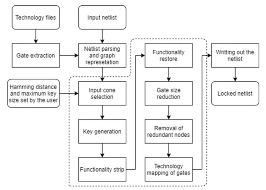
Figure 1.
An algorithm flowchart.
3.2. Graphical User Interface
The purpose of the graphical user interface shown in Figure 2 is to give the user a method to select the netlist intended for locking, the destination directory where the locked netlist and the generated key will be stored, as well as enter the necessary parameters for the SFLL-HD algorithm (Hamming distance h and maximum key size). It also provides a help section for the user to make himself/herself familiar with the algorithm and aforementioned parameters together with what type of netlist is suitable for the tool. If some of the inputs are missing or are not in the desired format (non-negative integer for h and maximum key size), the GUI gives an appropriate warning and stops the program from further execution. A warning can also be given in case the netlist contains inappropriate gates or if the Hamming distance h is larger than the input cone being protected. If all inputs were correct, the program starts running with a bar indicating its progress. After the program is finished, an info message is shown.
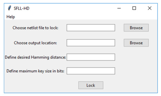
Figure 2.
Graphical user interface.
3.3. Graph Representation
The backbone of the development of this tool is the representation of the netlist as a directed acyclic graph. Nodes of the graph are all important elements of the netlist (gates, state elements, inputs, outputs, and wires) while edges demonstrate the connections between the nodes. The reason for wires to be represented as nodes and not edges is because, in the netlist, the connection between wires and gates is implemented through wire names, so the representation of wires as nodes reflects the implementation of the netlist in a more suitable manner. The graph has a name that represents the name of the module. Every node also has its name that reflects the indicator in the netlist as well as attributes for better representation of different node types:
- Attribute type—indicates the node type (gate, state_el, input, output, or wire).
- Attribute gate (only for gates and state elements)—indicates the name of the actual gate from the library.
- Attribute pinout (only for gates and state elements)—a list containing information about the gate or register pins and the wire, input, or output it is connected to.
The representation of the netlist as a graph is implemented with class DiGraph from the Python library networks.
The graph is formed from the netlist by taking all inputs, outputs, state elements, gates, and wires and transforming them into nodes in the graph. Connections between those elements are represented as edges in the graph.
3.4. Technology
The tool is designed to work with Verilog gate-level netlists that have been compiled by Design Compiler for Synopsis C35 library. All possible combinational gates or sequential elements are extracted from technology files and sorted into those two groups. Out of the gate group, appropriate NAND, NOR, XOR, and NOT gates are also selected and are going to be inserted into the circuit by the algorithm.
3.5. Netlist Parsing
The goal of netlist parsing, shown in Figure 3, is to identify the important features of the netlist such as gates, registers, wires, inputs, and outputs, which are necessary to represent the netlist as a graph. The first step is to break the netlist into sections separated by semicolons. Some of those sections will contain all the inputs, outputs, or wires, while others will contain individual gates and registers. After breaking the netlist into such sections, every section is further broken into strings separated by delimiters including spaces, commas, parentheses, and newlines, except for gate inputs and outputs where parentheses are taken with different consideration. These strings are necessary to identify the main features of the netlist. The name of a module being locked is extracted from the section starting with the module since it is the following string and is given as the name of the graph. Sections that start with input, output, or wire contain strings with names of all inputs, outputs, and wires respectively. Every string is given as a name of a new node with the type attribute given accordingly. The remaining sections are descriptions of individual gates or state elements. A unique identifier of the gate in the netlist is a second string in the section and is a name of a node. The first string in the section is a gate or state element name that should be present in the gate or state element list extracted from the technology file. The attribute type is given according to the presence in one of these lists, while the string itself is assigned to the attribute gate. The remaining strings describe connections the gate has with wires, inputs, and outputs, and the graph connections are constructed accordingly. Those strings also comprise the attribute pinout as a list.
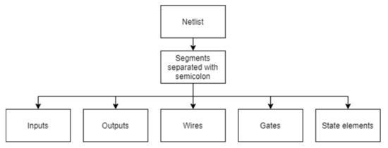
Figure 3.
Parsing process of the netlist.
3.6. Selection of an Input Cone to Lock
The SFLL-HD algorithm, shown in Figure 4, performs the logic locking on a single input cone, so the first step in the program should be the choice of the input cone to be locked. The program begins the search for the largest input cone (the one with the most inputs). However, because the sizes of the key and the protected input pattern are the same and there is the possibility of limiting the key size, the search is terminated upon finding the input cone greater than or equal to the key size. If the input cone is greater than the key size, only a set of its inputs equivalent to the key size will be included in a protected input pattern. The input cone, on the other hand, should not be smaller than the Hamming distance parameter h. This does not affect the program choice of an input cone, but in case the mentioned situation happens, the program will alert the user to modify the Hamming distance parameter to a suitable value.
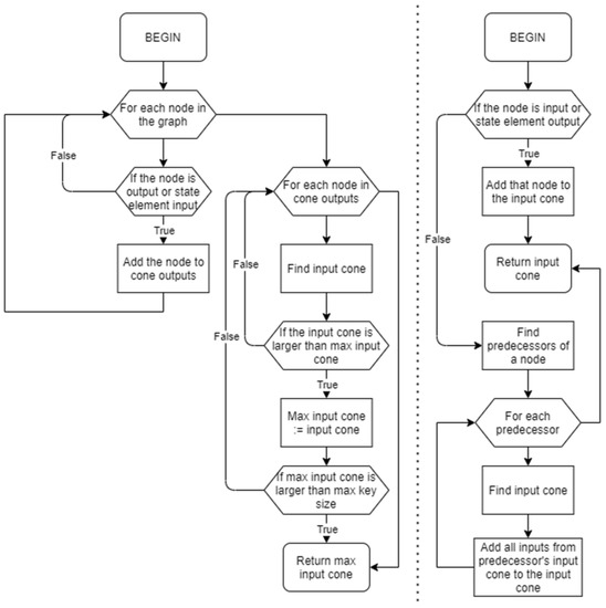
Figure 4.
The algorithm for finding a maximum input cone (left) and an input cone for a single node (right).
The procedure of finding the largest input logic cone starts with grouping all possible logic cone outputs (top module outputs—nodes of type output and state element inputs—and nodes of type wire which are predecessors of state_el nodes). The possible inputs of a cone are top module inputs (nodes of type input) and state element outputs (nodes of type wire which are successors of state_el nodes). For a specific logic cone output, the search for its input cone is a recursive function. The input cone of the desired node is a union of input cones of its predecessor nodes. The termination criterion is when a node is a possible input of a logic cone. Its input cone is that node itself.
3.7. Key Generation
After the input cone to be protected is selected, the program generates the secret key. The size of the key in bits is a smaller value between the size of the input cone and a user-defined maximum key value. The key is generated as a random number between zero and 2key size−1.
3.8. Functionality Strip
The first modification of the original netlist is a functionality strip function, shown in Figure 5, Its final goal is to invert the output of the logic cone for all input patterns which are a Hamming distance h from the correct key. The program iterates through all 2key size patterns and checks if its Hamming distance from the key is h. For such patterns, an AND gate is inserted. Its inputs are inputs of the logic cone, if the appropriate bit of the pattern is logic ‘1’ or the inverted inputs of the logic cone if the appropriate bit of the pattern is logic ‘0’. Outputs of all such created AND gates are fed to a newly inserted OR gate. The output of the OR gate is logic ‘1’ only for those input patterns of a Hamming distance h from the key. It is then fed to a new XOR gate whose other input is the output of the protected logic cone. The XOR gate output is then equal to the original logic cone output for input patterns with Hamming distance other than h and inverted logic cone output for input patterns with Hamming distance h from the key.
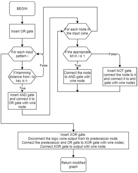
Figure 5.
The functionality strip function diagram.
3.9. Functionality Restore
Functionality stripped netlist is then additionally modified by a restore function, shown in Figure 6. Its purpose is to add another inversion of the logic cone output when the Hamming distance between the protected input cone and input key is h. If the input key is correct, it will cancel the inversion made by the functionality strip function for every input pattern. If the key is incorrect, it will cancel some of the inversions made by the functionality strip function, but will also create some additional inversions to previously non-inverted patterns.
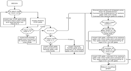
Figure 6.
The functionality restores the function diagram.
Exact key size XOR gates are inserted at the beginning of the functionality restore function. Inputs to each XOR gate are one bit from the input cone and one bit from the input key. The Hamming distance between the protected input cone and input key is reflected in the number of logic ones in the XOR gate outputs. The following function is true if the number of logic ones is h or less. There are ways to choose a combination of key size h XOR key gate outputs. For every combination, an OR gate is inserted whose inputs are selected key gate outputs. Outputs of all OR gates are then fed to a NAND gate. If the number of logic ones is h or less, there will be at least one OR gate with all logic zeros as inputs, and the whole function will output logic ‘1’. To create a function that is true only if the number of logic ones is exactly h, the previously explained function has to be XOR-ed with the same function that checks if the number of logic ones is h − 1 or less. Two exceptions are if h is 0 or is equal to key size. In the first case, the first function alone is sufficient, while in the second case, an AND function gives the desired behavior.
3.10. Gate Size Reduction
Since in the previous two steps some of the created gates can have more than four inputs, which is maximum in the technology the tool is supposed to work in, those gates have to be reduced to sufficiently small ones. A gate size reduction function, shown in Figure 7, is called as long as there are gates in the netlist with more than four inputs. The large gate is replaced with several 4-input gates whose outputs are fed to a single gate. Since that gate may still be larger than 4-input, the process has to repeat until there is no such gate, so we obtain a tree-like formation. For all gates except NAND and NOR gates, all replacement gates are of the same type as the original gate, to preserve the original functionality. If the original gate is NAND, it is replaced with several NAND gates fed to an OR gate, while a NOR gate is replaced with several NOR gates fed to an AND gate.
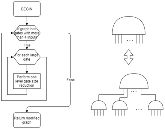
Figure 7.
A gate size reduction for the whole graph algorithm (left) and an example of one level gate size reduction (right). Redundant nodes removal.
All of the previous steps can generate gates with only one input, except for NOT gates. Such gates are not present in any technology and have to be replaced appropriately. NAND and NOR gates are replaced with NOT gates, while AND, OR, and XOR gates are simply removed. Upon removal of the gate node, its successor wire node also has to be removed, while the predecessor wire node is connected to the gate node succeeding the removed wire node, so the rerouted netlist is valid, as shown in Figure 8.
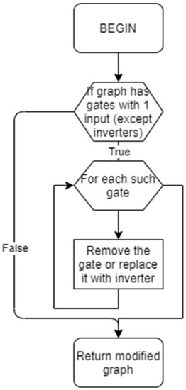
Figure 8.
Removal of redundant nodes.
3.11. Technology Mapping of the Gates
Gates inserted by the algorithm so far have only abstract attribute gates describing if it is an AND, OR, NAND, NOR, or XOR gate, unlike the gates in the original netlist where the same attribute is the name of the exact gate in the technology library. Since there are no AND or OR gates in the C35 library, such gates are first replaced. Every AND gate is replaced with a NAND gate and an inverter, while the OR gate is replaced with a NOR gate and an inverter. Afterward, gate attributes are updated with the selected names of the gates from the library depending on the type of the gate and the number of its inputs, as shown in Figure 9.
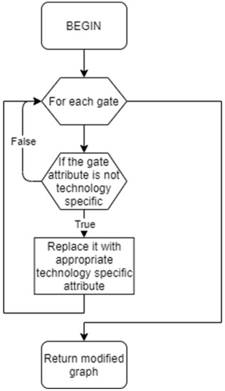
Figure 9.
Technology gate mapping.
3.12. Writing out the Locked Netlist
Writing out the netlist begins with identifying the module name, as well as all inputs, outputs, and wires from the nodes in the graph representation. A line with the module name and all its pins (inputs and outputs) is written out first. Then, the program writes out the lines with all inputs, outputs, and wires. Finally, the program writes out the information about every gate or state element, as shown in Figure 10.
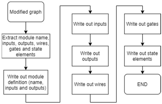
Figure 10.
Process of netlist generation from the graph.
It should be noted in this context that the number of nodes in the generated netlist is smaller compared to that of the original design, especially for locked circuits with a higher key-gate number. For example
3.13. Integration of the Tool with the IC Design Process
Integrated circuit design flow is a process of gradual refining and validation. During that process, a model on a high level of abstraction is translated to a detailed low-level structural model. The model of a design on the highest level of abstraction is a design specification. It can be in the form of a textual model, the algorithm flow graph, or in a structural form on a processor level. The model is then refined in a process called RTL design where an engineer describes the design in one of the hardware description languages—HDLs (VHDL, Verilog, System Verilog, …). The product of that process is an HDL file on the RTL level. The next refinement stage is the logic synthesis, which is performed by a synthesis tool such as Design Compiler. It is a process of mapping the RTL level design to the technology-specific gate-level netlist taking into consideration various optimizations and constraints such as timing, power, and area. The resulting gate-level netlist then goes through the final refinement stage—placement and routing. It is a process of deciding where to place library elements on a chip and how to design the connecting wires. This stage outputs the file in a format that can then be sent to the foundry for fabrication, as shown in Figure 11.
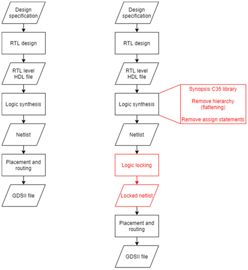
Figure 11.
A typical IC design flow (left) and IC design flow with logic locking (right).
The logic locking tool developed in this work fits in the IC design flow after logic synthesis and before placement and routing. Since the tool accepts only certain types of gate-level netlists, the synthesis stage must follow specific rules. In the current stage, the tool only accepts netlist files compiled for the Synopsis C35 library. The design also has to be flattened, i.e., its hierarchy has to be removed. It should also avoid having assigned statements. This results in a netlist consisting of only one module which will be locked. All other optimizations and constraints are allowed.
The netlist generated in such a manner is fed to the logic locking tool which outputs the locked netlist. That netlist is also a gate-level netlist and can be forwarded to the placement and routing stage in the same way as the original netlist when there is no logic locking stage. If the key insertion led to performance constraints violations, the user can fix it by applying physical optimization at the place and route stage to avoid the need for re-synthesis.
After the layout is sent to the foundry, it goes through a process of fabrication. It then passes through several levels of testing before being placed in a package. Without the logic locking stage, the integrated circuit after packaging would be fully functional and could be put on the market. However, when the locking process is involved, the IC has to go through the activation stage where the correct key is applied to become a functional IC, as shown in Figure 12.
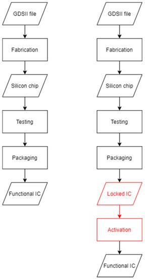
Figure 12.
IC fabrication and activation process.
4. Case Studies and Comparison of Overheads
4.1. Introduction
Several experiments have been conducted on the tool when it was used to lock various benchmark circuits. The conducted experiments demonstrated the correctness of the tool against the algorithm specification, evaluation of the level of protection it provides for varying parameters k and h, evaluation of performance and computational complexity for varying parameters k and h, and the number of nodes in the input netlist n, as well as comparison of area, power, and timing overheads, each being assessed for varying parameters k and h.
4.2. Computational Complexity and Performance Evaluation
The results of this analysis are shown in Figure 13, Figure 14, Figure 15, Figure 16 and Figure 17 respectively. The computational complexity of the program and its running time depending on several factors, most notably the number of nodes in the graph n, key size k, and binomial coefficient where h is a specified Hamming distance. As was previously mentioned, the number of nodes includes all the inputs, outputs, gates, wires, and state elements in the circuit. The number of nodes, however, is dependent on both k and h. In this part, we will focus on two distinct parts of the program: the first being the locking algorithm which transforms the graph model of the original netlist into the graph model of the locked netlist (from functionality strip to technology mapping in Figure 1), while the second one is the netlist write-out function. The reason for this is that these two functions can be the bottleneck of the performance of the whole program.
Figure 13.
Execution time of the locking algorithm against the number of nodes after the final stage of locking for different values of k and h.
Figure 14.
Execution time of the locking algorithm against the number of nodes in the original netlist.
Figure 15.
Execution time of the netlist write-out function against the number of nodes.
Figure 16.
Execution time of the locking algorithm against h, increasing k when h = 0 causes exponential execution time increase in a program because there is a loop in implementation that iterates 2k times and executes the body (k h) times. In the case of h = 0, the number of iterations causes the exponential execution time.
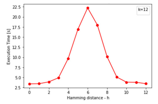
Figure 17.
Execution time of the locking algorithm against k.
(1) Dependence on the number of nodes: since the purpose of the program is to insert additional logic to ensure logic locking, the number of nodes in the graph changes during the run time of the program. The functionality strip and restore functions do not depend on the number of nodes in the graph. However, those two functions insert a significant number of new nodes. The functionality strip function inserts approximately nodes while the restore function adds new nodes to the graph. Some of the inserted gates may be too large to be implemented from the library and will have to be reduced. One gate can have up to inputs. One iteration of the gate reduction function iterates through all currently present nodes in the graph. The number of iterations, however, is equal to . The node removal function iterates through all nodes once and removes some of them, while technology mapping iterates through all nodes twice and inserts some nodes if necessary. Since the number of nodes in different stages is not constant, we have to approximate the computational complexity over one particular stage. If it is the final stage, this means that the number of nodes n is the number of nodes after the algorithm has finished locking. The dependence of the locking algorithm on the number of nodes can then be expressed as since both k and h are constants.
The netlist write-out function traverses through all nodes of the locked netlist exactly two times, thus having the linear computational complexity of O (n).
(2) Dependence on key size k and Hamming distance h: when analyzing the dependence of the computational complexity of the locking algorithm, key size k, and Hamming distance h cannot be observed separately. This is because the algorithm has a strong dependence on the binomial coefficient . Two functions of the algorithm are bottlenecks when it comes to performance against those parameters. A part of the functionality strip function is a loop that iterates 2k times. However, the condition to enter the loop body is satisfied times. This coefficient is highest when h is exactly k/2 and is lower when it is closer to 0 or k. If the execution time of the iteration when the condition is not satisfied is t0 and when the condition is satisfied is t1 (t1 > t0), the total execution time of the loop is . This means that if the binomial coefficient is low, the decisive parameter for the performance is k, while if the coefficient is high, it is the main factor for function performance. Similarly, the restore function also has a loop that iterates 2k times with the condition to enter the body of the loop. However, the condition in the restore function is satisfied times except in boundary cases when h is equal to 0 or k, when this number is and respectively. When the number of times this condition is satisfied is comparable to the number of total iterations, the program execution time will linearly depend on the binomial coefficient , while when that number is negligible the complexity is O (2k).
4.3. Functional Verification
To prove that the netlist produced by the tool implements its intended functionality, the netlist can be verified by simulation in Modelsim as shown in Figure 18 and Figure 19. The verification environment consists of the original and locked netlists and a test bench that applies a key to the locked netlist drive inputs and observes outputs of both netlists and checks the difference between those outputs. The goal is to prove that for the correct key, the output is the same for all input patterns on the original and locked circuit. For wrong keys, the output should be inverted if the Hamming distance between the input pattern and the correct key is h or the Hamming distance between the input pattern and the applied key is h.
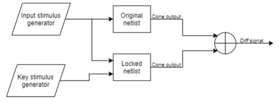
Figure 18.
Verification environment.
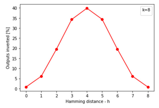
Figure 19.
Corruptibility of outputs.
The circuit chosen for simulation is the C432 benchmark circuit from the ISCAS85 benchmark set. The circuit is locked with 8 bits for key and Hamming distance of 2. As it can be seen from, Figure 20 and Figure 21, when the correct key is applied, signals out from the original netlist and out from the locked netlist are always the same, and signal diff, which represents their difference is zero disregarding occasional glitches. If the incorrect key is applied, that signal becomes one for some input patterns, as was expected.
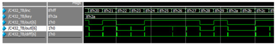
Figure 20.
Output signals of the original and locked netlists for the correct key.
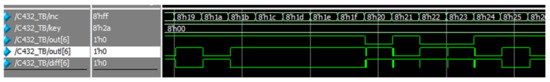
Figure 21.
Output signals of the original and locked netlists for the incorrect key.
4.4. Security Evaluation
When evaluating the security of the algorithm and the tool, we have to take into consideration, three main attack families. The algorithm should be resilient to SAT attacks, sensitization attacks, and removal attacks. As was already mentioned in Table 1 and proven in [14], the algorithm is resilient to sensitization attacks and its corruptibility and resilience to SAT and removal attacks can be configured with parameter h. Values of h closer to 0 or key size k make the algorithm more resilient to SAT attacks, while values closer to k/2 provide better corruptibility and resilience to removal attacks. While resilience to SAT attacks cannot be demonstrated with a simulation, corruptibility and thus removal attacks resilience can.
Similar to the functional verification part, the environment is set as in Figure 18 and the simulation is performed in Modelsim. The circuit chosen for simulation is the C432 benchmark circuit from the ISCAS85 benchmark set. It is locked with 8 bits for key and various values for Hamming distance. An incorrect key is applied to the locked netlist and diff signal, which is logic one when the inverted cone output is observed for various input patterns and the number of times the output is inverted is recorded. The best corruptibility is achieved when the diff signal is one 50% of the time since the attacker cannot guess whether the output was inverted or not. Figure 19 shows experimental results for this configuration.
4.5. Comparison of Overheads
The results are shown in Figure 22, Figure 23, Figure 24, Figure 25 and Figure 26. The process of logic locking inserts additional logic in the design which can affect the performance. Synthesis tool Design Compiler can measure parameters such as area, power usage, and timing (delay of the critical path) of the netlist which indicate the performance of the circuit. To analyze the effect of the locking process on the performance, two benchmark circuits from the ISCAS85 benchmark set (C432 and C7552) were locked with different values of key size k and Hamming distance h, their area, power usage, and critical path delay were calculated and plotted against locking parameters k and h.
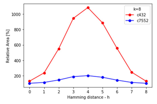
Figure 22.
Relative area increase in locked netlists for different values of Hamming distance.
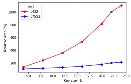
Figure 23.
Relative area increase of locked netlists for different values of key size.
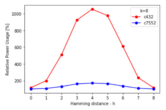
Figure 24.
Relative power usage increase in locked netlists for different values of Hamming distance.
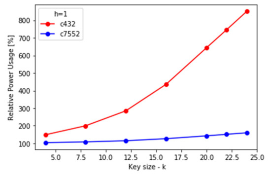
Figure 25.
Relative power usage increase in locked netlists for different values of key size.
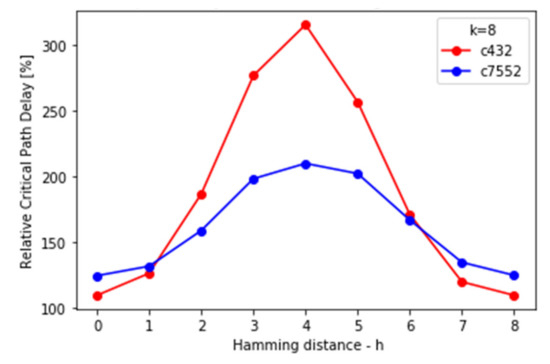
Figure 26.
Relative critical path delay increase in locked netlists for different values of Hamming distance.
(1) Area: The main factor that causes area overhead was the addition of new gates in the functionality strip and Restore functions. The number of added gates is proportional to and , respectively, as it was explained previously. This means that the area overhead will depend more on the coefficient than on key size k.
Areas of the original netlists are 8374.4 μm2 for C432 and 80,456.8 μm2 for C7552. As can be seen from Figure 22 and Figure 23, the relative increase in area is much more significant for C432 since it is a smaller circuit and the absolute increase mostly depends on parameters k and h. It is highest when h is equal to k/2 and for a constant h it grows linearly with k as it was expected
(2) Power: power dissipation consists of internal cell power, net switching power, and leakage power. Since all three elements increase with an increased number of gates, the experimental results are expected to be similar to those of area overhead. Power dissipations of the original netlists are 2.274 mW for C432 and 30.208 mW for C7552.
Similarly to area increase, the relative power dissipation increase was more significant for the originally smaller circuit, peaks for h = k/2, and grows linearly with k.
(3) Timing: to estimate the overhead caused by the locking process on the timing, a delay of the critical path will be used as a measure. The critical path is a path without state elements (only combinatorial gates) with the longest delay. Unlike area and power dissipation, critical path delay does not only depend on the number of inserted gates but also where those gates were inserted. Critical path delays of the original netlists are 19.37 ns for C432 and 24.73 ns for C7552.
As can be seen from Figure 26 and Figure 27, the relative increase in the critical path delay is not as severe as in area and power usage for smaller C432, while it is similar for larger C7552. The relative delay increase also peaks for h = k/2 and C432 grows linearly with k, while for C7552 it stays still after a minor increase.
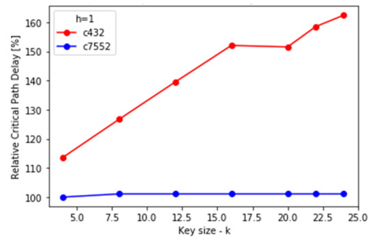
Figure 27.
Relative critical path delay increase in locked netlists for different values of key size.
5. Conclusions
This work has presented a framework to automate the logic locking process, hence making it an integral part of the IC design flow. This is achieved through the design and implementation of standalone software that performs logic locking based on the SFLL-HD algorithm. The latter was chosen following a rigorous analysis of the literature. The paper has also presented a detailed case study demonstrating how the developed software can be integrated with existing design processes. The tool in its current form is a standalone software that can easily be adopted by IP developers to mitigate the risks of design piracy and can be downloaded from [27]. Future extensions include performance optimization by reducing exponential dependency on k. Another possible extension is to integrate the tool with the digital synthesis flow using industry-standard tools, such as the design compiler from Synopsis and the RTL compiler from Cadence.
Author Contributions
N.K. (tool development and paper writing). B.H. (Supervision, Research and paper writing). Y.Z. (Paper writing). All authors have read and agreed to the published version of the manuscript.
Funding
This research was partly funded by the royal academy of engineering (grant No. IF2021\36).
Conflicts of Interest
The authors declare no conflict of interest.
References
- Roy, J.A.; Koushanfar, F.; Markov, I.L. EPIC: Ending Piracy of Integrated Circuits. In Proceedings of the 2008 Design, Automation and Test in Europe, Munich, Germany, 10–14 March 2008; pp. 1069–1074. [Google Scholar]
- Chakraborty, R.S.; Bhunia, S. HARPOON: An Obfuscation-Based SoC Design Methodology for Hardware Protection. IEEE Trans. Comput. Des. Integr. Circuits Syst. 2009, 28, 1493–1502. [Google Scholar] [CrossRef]
- Engels, S.; Hoffmann, M.; Paar, C. The End of Logic Locking? A Critical View on the Security of Logic Locking. IACR Cryptol. ePrint Arch. 2019, 2019, 796. [Google Scholar]
- Rajendran, J.; Pino, Y.; Sinanoglu, O.; Karri, R. Security analysis of logic obfuscation. In Proceedings of the 49th Annual Design Automation Conference on—DAC’12, San Francisco, CA, USA, 3–7 June 2012; pp. 83–89. [Google Scholar]
- Rajendran, J.; Zhang, H.; Zhang, C.; Rose, G.; Pino, Y.; Sinanoglu, O.; Karri, R. Fault Analysis-Based Logic Encryption. IEEE Trans. Comput. 2013, 64, 410–424. [Google Scholar] [CrossRef]
- Subramanyan, P.; Ray, S.; Malik, S. Evaluating the security of logic encryption algorithms. In Proceedings of the 2015 IEEE International Symposium on Hardware Oriented Security and Trust (HOST), Washington, DC, USA, 5–7 May 2015; pp. 137–143. [Google Scholar]
- Shamsi, K.; Li, M.; Meade, T.; Zhao, Z.; Pan, D.Z.; Jin, Y. Cyclic Obfuscation for Creating SAT-Unresolvable Circuits. In Proceedings of the Great Lakes Symposium on VLSI 2017, Banff, AB, Canada, 10 May 2017; pp. 173–178. [Google Scholar]
- Zhou, H.; Jiang, R.; Kong, S. CycSAT: SAT-based attack on cyclic logic encryptions. In Proceedings of the 2017 IEEE/ACM International Conference on Computer-Aided Design (ICCAD), Irvine, CA, USA, 13–16 November 2017; pp. 49–56. [Google Scholar]
- Xie, Y.; Srivastava, A. Anti-SAT: Mitigating SAT Attack on Logic Locking. IEEE Trans. Comput. Des. Integr. Circuits Syst. 2018, 38, 199–207. [Google Scholar] [CrossRef]
- Yasin, M.; Mazumdar, B.; Rajendran, J.J.V.; Sinanoglu, O. SARLock: SAT attack resistant logic locking. In Proceedings of the 2016 IEEE International Symposium on Hardware Oriented Security and Trust (HOST), McLean, VA, USA, 3–5 May 2016; pp. 236–241. [Google Scholar]
- Yasin, M.; Mazumdar, B.; Sinanoglu, O.; Rajendran, J. Security analysis of Anti-SAT. In Proceedings of the 2017 22nd Asia and South Pacific Design Automation Conference (ASP-DAC), Chiba, Japan, 16–19 January 2017; pp. 342–347. [Google Scholar]
- Yasin, M.; Mazumdar, B.; Sinanoglu, O.; Rajendran, J. Removal Attacks on Logic Locking and Camouflaging Techniques. IEEE Trans. Emerg. Top. Comput. 2020, 8, 517–532. [Google Scholar] [CrossRef] [Green Version]
- Yasin, M.; Sengupta, A.; Schafer, B.C.; Makris, Y.; Sinanoglu, O.; Rajendran, J. What to Lock? Functional and Parametric Locking. In Proceedings of the Great Lakes Symposium on VLSI 2017, Banff, AB, Canada, 10 May 2017. [Google Scholar]
- Yasin, M.; Sengupta, A.; Nabeel, M.T.; Ashraf, M.; Rajendran, J.; Sinanoglu, O. Provably-Secure Logic Locking: From Theory to Practice. In Proceedings of the 2017 ACM SIGSAC Conference on Computer and Communications Security, Dallas, TX, USA, 30 October 2017. [Google Scholar]
- Yasin, M.; Zhao, C.; Rajendran, J.J. SFLL-HLS: Stripped-Functionality Logic Locking Meets High-Level Synthesis. In Proceedings of the 2019 IEEE/ACM International Conference on Computer-Aided Design (ICCAD), Westminster, CO, USA, 4–7 November 2019; pp. 1–4. [Google Scholar]
- Pilato, C.; Chowdhury, A.B.; Sciuto, D.; Garg, S.; Karri, R. ASSURE: RTL Locking Against an Untrusted Foundry. IEEE Trans. Very Large Scale Integr. (VLSI) Syst. 2021, 29, 1306–1318. [Google Scholar] [CrossRef]
- Šišejković, D.; Merchant, F.; Reimann, L.M.; Leupers, R.; Kegreiß, S. Scaling Logic Locking Schemes to Multi-module Hardware Designs. In International Conference on Architecture of Computing Systems; Springer Science and Business Media LLC: Berlin/Heidelberg, Germany, 2020; pp. 138–152. [Google Scholar]
- Chakraborty, P.; Cruz, J.; Bhunia, S. SAIL: Machine Learning Guided Structural Analysis Attack on Hardware Obfuscation. In Proceedings of the 2018 Asian Hardware Oriented Security and Trust Symposium (AsianHOST), Hong Kong, China, 17–18 December 2018; pp. 56–61. [Google Scholar]
- Alaql, A.; Forte, D.; Bhunia, S. Sweep to the Secret: A Constant Propagation Attack on Logic Locking. In Proceedings of the 2019 Asian Hardware Oriented Security and Trust Symposium (AsianHOST), Xi’an, China, 16–17 December 2019; pp. 1–6. [Google Scholar]
- Šišejković, D.; Merchant, F.; Reimann, L.M.; Leupers, R.; Giacometti, M.; Kegreiß, S. A secure hardware-software solution based on RISC-V, logic locking, and microkernel. In Proceedings of the 23rd International Workshop on Software and Compilers for Embedded Systems, St. Goar, Germany, 25 May 2020; pp. 62–65. [Google Scholar]
- Sisejkovic, D.; Merchant, F.; Leupers, R.; Ascheid, G.; Kegreiss, S. Inter-Lock: Logic Encryption for Processor Cores Beyond Module Boundaries. In Proceedings of the 2019 IEEE European Test Symposium (ETS), Baden-Baden, Germany, 27–31 May 2019; pp. 1–6. [Google Scholar] [CrossRef]
- Šišejković, D.; Merchant, F.; Leupers, R.; Ascheid, G.; Kegreiss, S. Control-lock: Securing processor cores against software-controlled hardware trojans. In Proceedings of the 2019 on Great Lakes Symposium on VLSI, Tysons Corner, VA, USA, 13 May 2019; pp. 27–32. [Google Scholar]
- Sisejkovic, D.; Merchant, F.; Leupers, R.; Ascheid, G.; Kiefer, V. A Critical Evaluation of the Paradigm Shift in the Design of Logic Encryption Algorithms. In Proceedings of the 2019 International Symposium on VLSI Design, Automation and Test (VLSI-DAT), Hsinchu, Taiwan, 22–25 April 2019; pp. 1–4. [Google Scholar] [CrossRef]
- Yang, F.; Tang, M.; Sinanoglu, O. Stripped Functionality Logic Locking With Hamming Distance-Based Restore Unit (SFLL-hd)—Unlocked. IEEE Trans. Inf. Forensics Secure. 2019, 14, 2778–2786. [Google Scholar] [CrossRef]
- Sirone, D.; Subramanyan, P. Functional Analysis Attacks on Logic Locking. IEEE Trans. Inf. Forensics Secure. 2020, 15, 2514–2527. [Google Scholar] [CrossRef] [Green Version]
- Duvalsaint, D.; Jin, X.; Niewenhuis, B.; Blanton, R.D. Characterization of Locked Combinational Circuits via ATPG. In Proceedings of the 2019 IEEE International Test Conference (ITC), Washington, DC, USA, 9–15 November 2019; pp. 1–10. [Google Scholar]
- Halak, B. Lockit: A Logic Locking Tool. Available online: https://www.researchgate.net/publication/353195333_Source_Code_for_The_Lockit_Tool (accessed on 13 September 2021).
Publisher’s Note: MDPI stays neutral with regard to jurisdictional claims in published maps and institutional affiliations. |
© 2021 by the authors. Licensee MDPI, Basel, Switzerland. This article is an open access article distributed under the terms and conditions of the Creative Commons Attribution (CC BY) license (https://creativecommons.org/licenses/by/4.0/).