
Influences of the Temperature on the Electrical Properties of HfO2-Based Resistive Switching Devices

 ,
,  , ,
, ,  ,
,  , , and
Abstract
:
1. Introduction
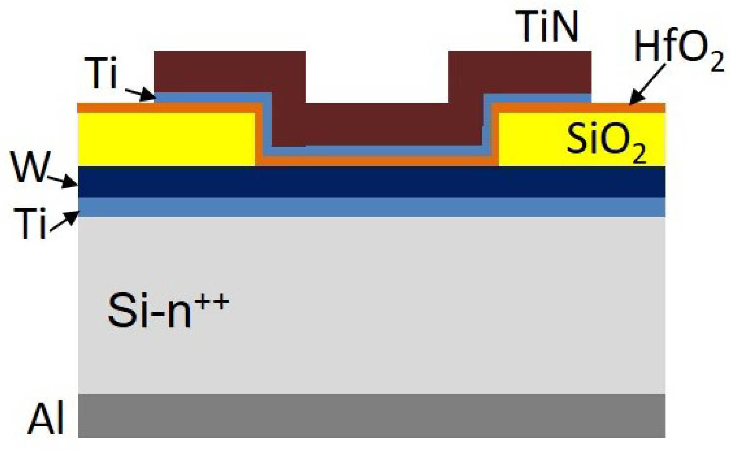
2. Experimental
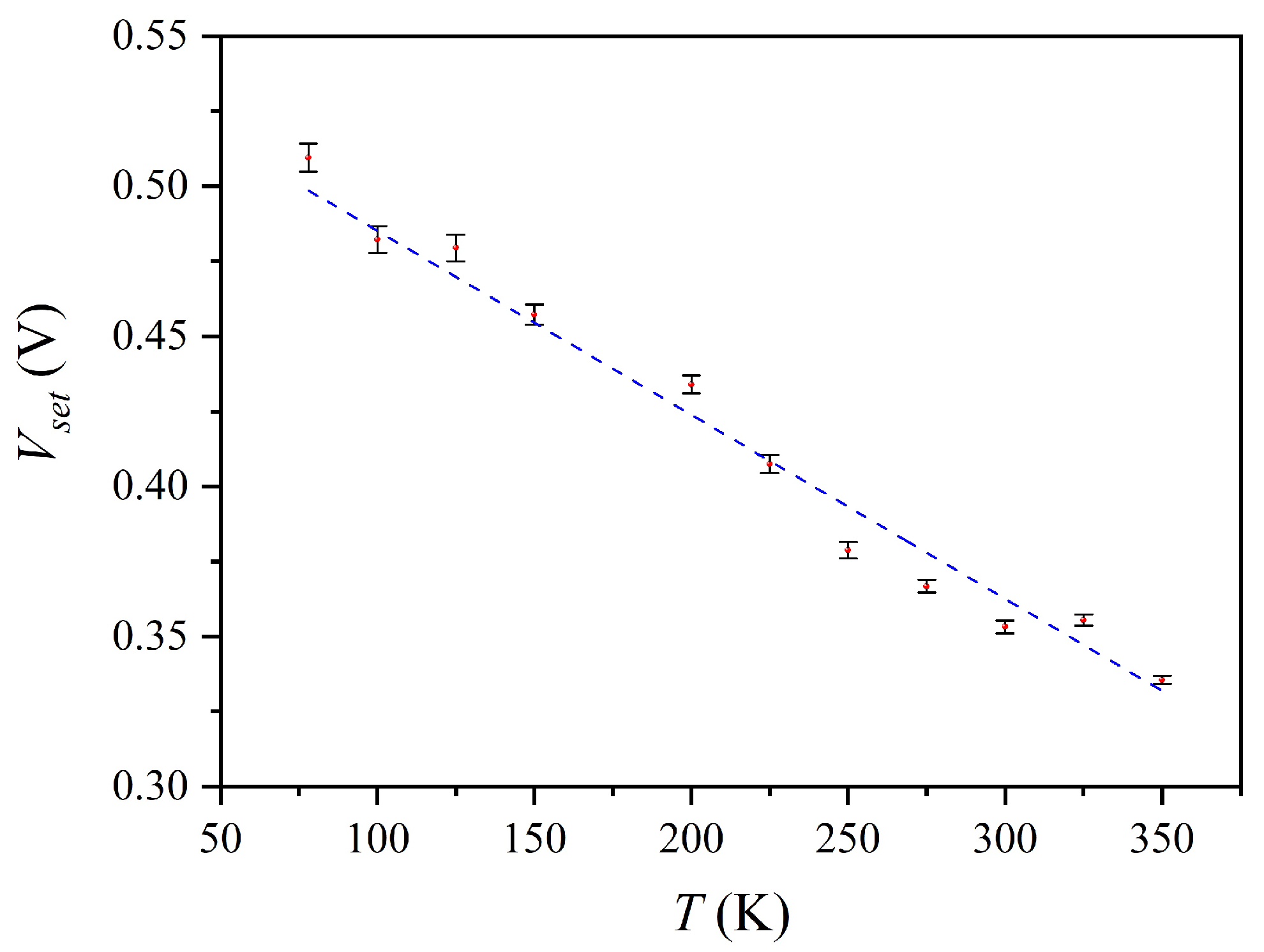
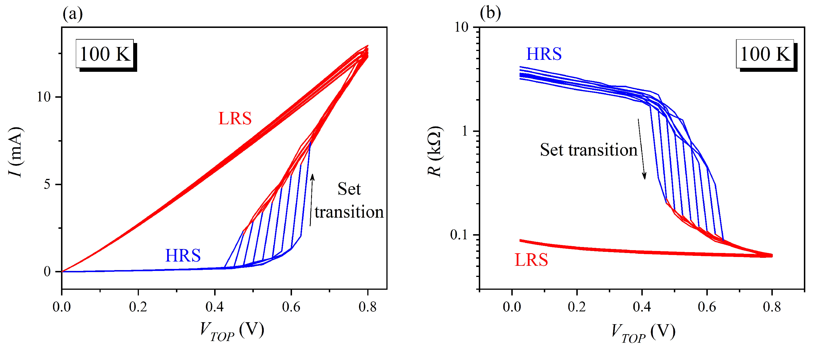
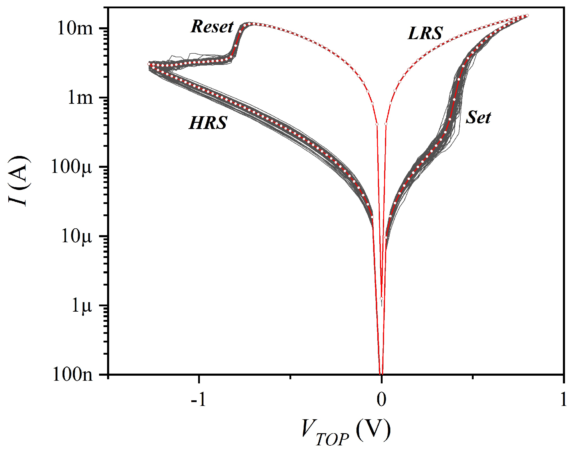
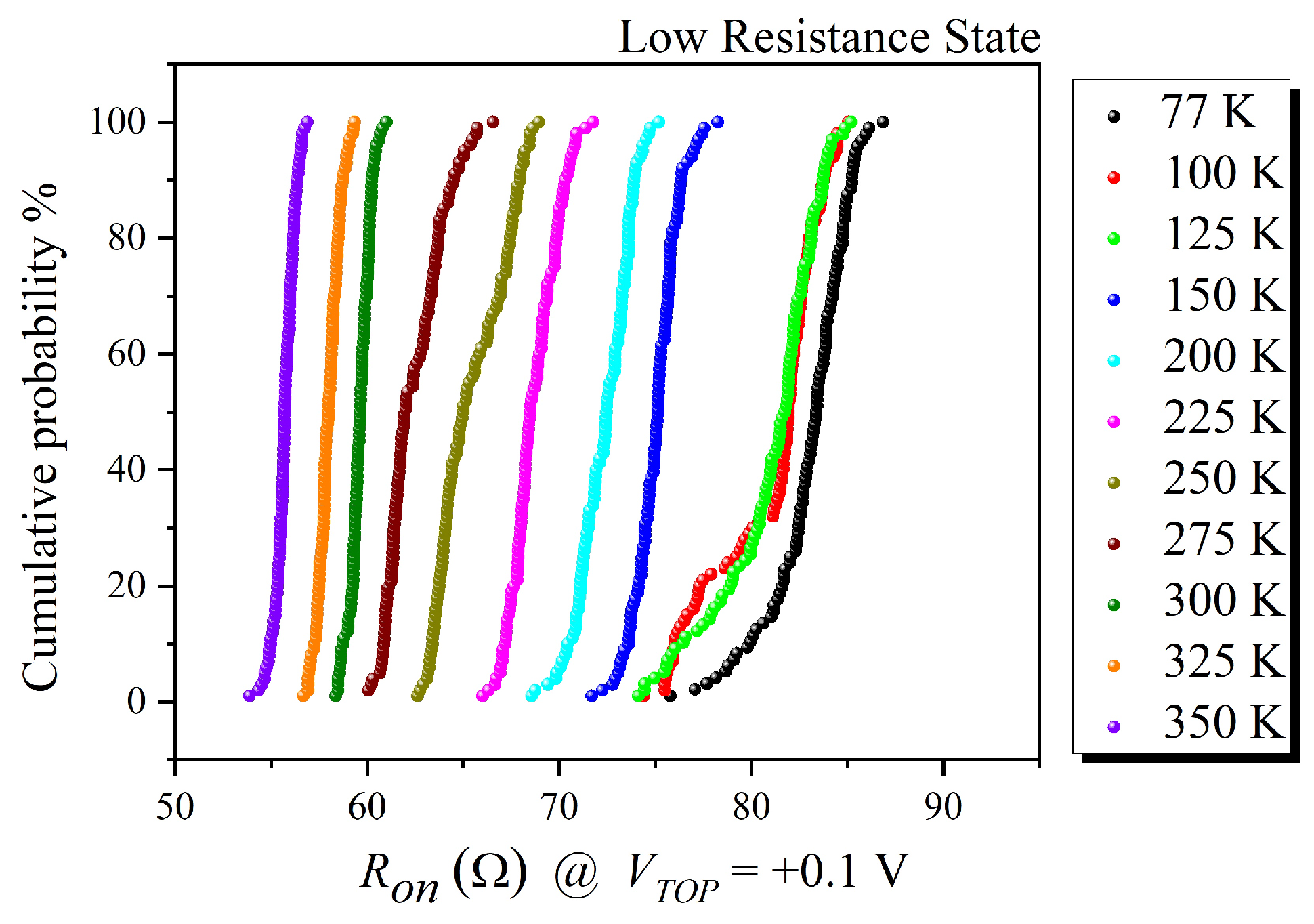
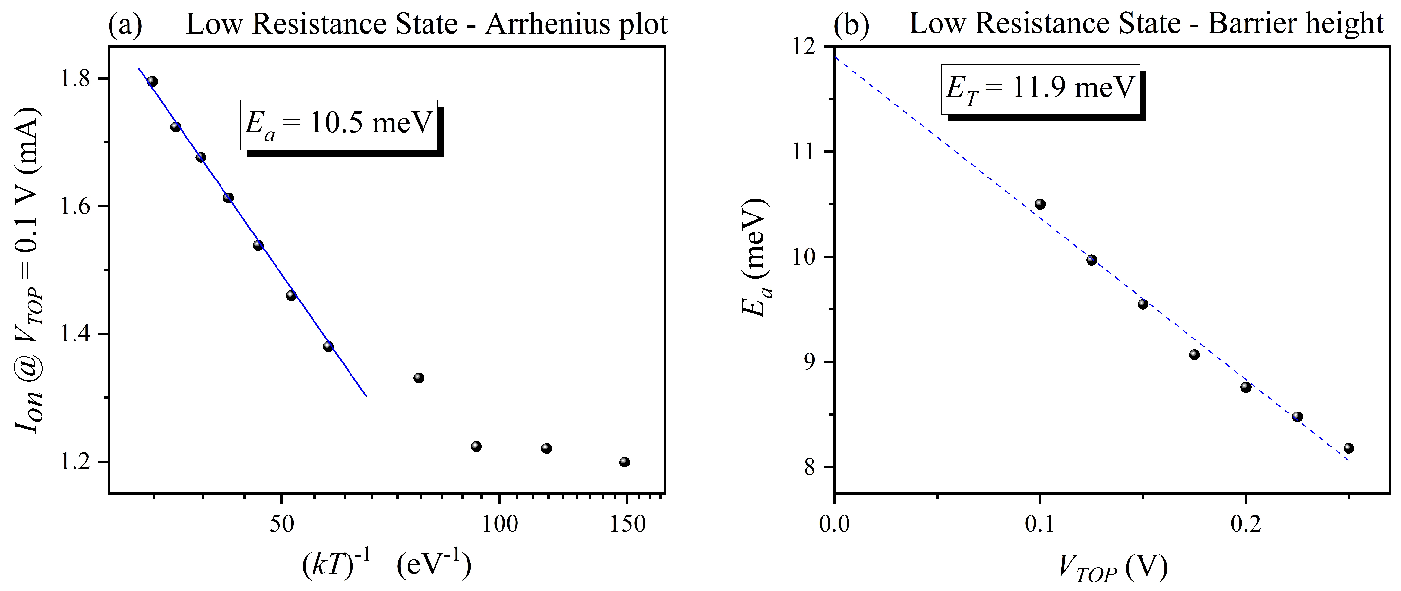
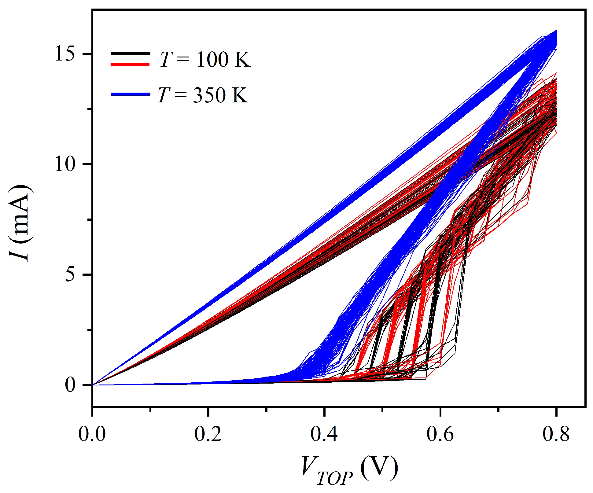
3. Results and Discussion
4. Conclusions
Author Contributions
Funding
Conflicts of Interest
References
- Slesazeck, S.; Mikolajick, T. Nanosclae resistive switching memory devices: A review. Nanotechnology 2019, 30, 352003. [Google Scholar] [CrossRef]
- Wang, Z.; Wu, H.; Burr, G.W.; Hwang, C.S.; Wang, K.L.; Xia, Q.; Yang, J.J. Resistive switching materials for information processing. Nat. Rev. Mater. 2020, 5, 173–195. [Google Scholar] [CrossRef]
- Zahoor, F.; Zulkifli, T.Z.A.; Khanday, F.A. Resistive Random Access Memory (RRAM): An Overview of Materials, Switching Mechanism, Performance, Multilevel Cell (mlc) Storage, Modeling, and Applications. Nanoscale Res. Lett. 2020, 15, 90. [Google Scholar] [CrossRef] [PubMed]
- Banerjee, W. Challenges and Applications of Emerging Nonvolatile Memory Devices. Electronics 2020, 9, 1029. [Google Scholar] [CrossRef]
- Chakraborty, I.; Jaiswal, A.; Saha, A.K.; Gupta, S.K.; Roy, K. Pathways to efficient neuromorphic computing with non-volatile memory technologies. Appl. Phys. Rev. 2020, 7, 021308. [Google Scholar] [CrossRef]
- Wu, X.; Yu, H.; Cao, J. Unraveling the origin of resistive switching behavior in organolead halide perovskite based memory devices. AIP Adv. 2020, 10, 085202. [Google Scholar] [CrossRef]
- Román Acevedo, W.; Rubi, D.; Lecourt, J.; Lüders, U.; Gomez-Marlasca, F.; Granell, P.; Golmar, F.; Levy, P. Manganite-based three level memristive devices with self-healing capability. Phys. Lett. A 2016, 380, 2870–2875. [Google Scholar] [CrossRef] [Green Version]
- Cheong, K.Y.; Tayeb, I.A.; Zhao, F.; Abdullah, J.M. Review on resistive switching mechanisms of bio-organic thin film for non-volatile memory application. Nanotechnol. Rev. 2021, 10, 680–709. [Google Scholar] [CrossRef]
- Carlos, E.; Branquinho, R.; Martins, R.; Kiazadeh, A.; Fortunato, E. Recent Progress in Solution-Based Metal Oxide Resistive Switching Devices. Adv. Mater. 2020, 33, 2004328. [Google Scholar] [CrossRef] [PubMed]
- Bersuker, G.; Gilmer, D.C.; Veksler, D. Metal-oxide resistive random access memory (RRAM) technology: Material and operation details and ramifications. In Advances in NON-Volatile Memory and Storage Technology; Magyari-Köpe, B., Nishi, Y., Eds.; Elsevier: Amsterdam, The Netherlands, 2019; pp. 35–102. [Google Scholar] [CrossRef]
- Giovinazzo, C.; Sandrini, J.; Shahrabi, E.; Celik, O.T.; Leblebizi, Y.; Ricciardi, C. Analog Control of Retainable Resistance Multistates in HfO2 Resistive-Switching Random Access Memories (ReRAMs). ACS Appl. Electron. Mater. 2019, 1, 900–909. [Google Scholar] [CrossRef]
- Fang, R.; Chen, W.; Gao, L.; Yu, W.; Yu, S. Low-Temperature Characteristics of HfOx-Based Resistive Random Access Memory. IEEE Electron. Device Lett. 2015, 36, 567–569. [Google Scholar] [CrossRef]
- Liu, Y.; Ouyang, S.; Yang, J.; Tang, M.; Wang, W.; Li, G.; Zou, Z.; Liang, Y.; Li, Y.; Xiao, Y.; et al. Effect of film thickness and temperature on the resistive switchingcharacteristics of the Pt/HfO2/Al2O3/TiN structure. Solid-State Electron. 2020, 173, 107880. [Google Scholar] [CrossRef]
- Rodríguez-Fernández, A.; Aldana, S.; Campabadal, F.; Suñé, J.; Miranda, E.; Jiménez-Molinos, F.; Roldán, J.B.; González, M.B. Resistive Switching with Self-Rectifying Tunability and Influence of the Oxide Layer Thickness in Ni/HfO2/n+-Si. IEEE Trans. Electron. Devices 2017, 64, 3159–3166. [Google Scholar] [CrossRef]
- Kumar Lata, L.; Jain, P.K.; Chand, U.; Bhatia, D.; Shariq, M. Resistive switching characteristics of HfO2 based bipolar nonvolatile RRAM cell. In Materials Today: Proceedings; Arora, M., Kumar Jain, P., Zafar, R., Vyas, R., Eds.; Elsevier: Amsterdam, The Netherlands, 2020; Volume 30, pp. 217–220. [Google Scholar] [CrossRef]
- Walczyk, C.; Walczyk, D.; Schroeder, T.; Bertaud, T.; Sowinska, M.; Lukosius, M.; Fraschke, M.; Wolansky, D.; Tillack, B.; Miranda, E.; et al. mpact of Temperature on the Resistive Switching Behavior of Embedded HfO2-Based RRAM Devices. IEEE Trans. Electron. Devices 2011, 58, 3124–3131. [Google Scholar] [CrossRef]
- Nakajima, R.; Azuma, A.; Yoshida, Y.; Shimizu, T.; Ito, T.; Shingubara, S. Hf layer thickness dependence of resistive switching characteristics of Ti/Hf/HfO2/Au resistive random access memory device. Jpn. J. Appl. Phys. 2018, 57, 06HD06. [Google Scholar] [CrossRef] [Green Version]
- Wang, Y.; Liu, Q.; Long, S.; Wang, W.; Zhang, M.; Zhang, S.; Li, Y.; Zuo, Q.; Yang, J. Investigation of resistive switching in Cu-doped HfO2 thin film for multilevel non-volatile memory applications. Nanotechnology 2009, 21, 045202. [Google Scholar] [CrossRef] [PubMed]
- Molina, J.; Torres, R.; Ranjan, A.; Pey, K.-L. Resistive switching characteristics of MIM structures based on oxygen-variable ultra-thin HfO2 and fabricated at low temperature. Mater. Sci. Semicond. Process. 2017, 66, 191–199. [Google Scholar] [CrossRef]
- González-Cordero, G.; González, M.B.; García, H.; Campabadal, F.; Dueñas, S.; Castán, H.; Jiménez-Molinos, F.; Roldán, J.B. A physically based model for resistive memories including a detailed temperature and variability description. Microelectron. Eng. 2017, 178, 26–29. [Google Scholar] [CrossRef]
- Waser, R.; Dittmann, R.; Staikov, G.; Szot, K. Redox-Based Resistive Switching Memories—Nanoionic Mechanisms, Prospects, and Challenges. Adv. Mater. 2009, 21, 2632–2663. [Google Scholar] [CrossRef]
- Fang, Z.; Wang, X.P.; Sohn, J.; Weng, B.B.; Zhang, Z.P.; Chen, Z.X.; Tang, Y.Z.; Lo, G.-Q.; Provine, J.; Wong, S.S.; et al. The Role of Ti Capping Layer in HfOx-Based RRAM Devices. IEEE Electron. Device Lett. 2014, 35, 912–914. [Google Scholar] [CrossRef]
- Guo, X.; Schindler, C.; Menzel, S.; Waser, R. Understanding the switching-off mechanism in Ag+ migration based resistively switching model systems. Appl. Phys. Lett. 2007, 91, 133513. [Google Scholar] [CrossRef] [Green Version]
- Wang, C.; Wu, H.; Gao, B.; Zhang, T.; Yang, Y.; Qian, H. Conduction mechanisms, dynamics and stability in ReRAMs. Microelectron. Eng. 2018, 187, 121–133. [Google Scholar] [CrossRef]
- Chen, K.-H.; Zhang, R.; Chang, T.-C.; Tsai, T.-M.; Chang, K.-C.; Lou, J.C.; Young, T.-F.; Chen, J.-H.; Shih, C.-C.; Tung, C.-W.; et al. Hopping conduction distance dependent activation energy characteristics of Zn:SiO2 resistance random access memory devices. Appl. Phys. Lett. 2013, 102, 133503. [Google Scholar] [CrossRef] [Green Version]
- Xu, X.-X.; Luo, Q.; Gong, T.-C.; Lv, H.-B.; Liu, Q.; Liu, M. Resistive switching memory for high density storage and computing. Chin. Phys. B 2021, 30, 058702. [Google Scholar] [CrossRef]
- Kim, Y.-M.; Lee, J.-S. Reproducible resistance switching characteristics of hafnium oxide-based nonvolatile memory devices. J. Appl. Phys. 2008, 104, 114115. [Google Scholar] [CrossRef]
- Yu, S.; Guan, X.; Wong, H.-S.P. Conduction mechanism of TiN/HfOx/Pt resistive switching memory: A trap-assisted-tunneling model. Appl. Phys. Lett. 2011, 99, 0635507. [Google Scholar] [CrossRef]
- Lin, C.-Y.; Wang, S.-Y.; Lee, D.-Y.; Tseng, T.-Y. Electrical Properties and Fatigue Behaviors of ZrO2 Resistive Switching Thin Films. J. Electrochem. Soc. 2008, 155, H615–H619. [Google Scholar] [CrossRef]
- García, H.; Vinuesa, G.; Ossorio, O.G.; Sahelices, B.; Castán, H.; Dueñas, S.; González, M.B.; Campabadal, F. Study of the set and reset transitions in HfO2-based ReRAM devices using a capacitor discharge. Solid-State Electron. 2021, 183, 108113. [Google Scholar] [CrossRef]
- Fleck, K.; La Torre, C.; Aslam, N.; Hoffmann-Eifert, S.; Böttger, U.; Menzel, S. Uniting Gradual and Abrupt SET Processes in Resistive Switching Oxides. Phys. Rev. Appl. 2016, 6, 064015. [Google Scholar] [CrossRef] [Green Version]
- Cüppers, F.; Menzel, S.; Bengel, C.; Hardtdegen, A.; von Witzleben, M.; Bötger, U.; Waser, R.; Hoffmann-Eifert, S. Exploiting the switching dynamics of HfO2-based ReRAM devices for reliable analog memristive behavior. APL Mater. 2019, 7, 091105. [Google Scholar] [CrossRef] [Green Version]


Publisher’s Note: MDPI stays neutral with regard to jurisdictional claims in published maps and institutional affiliations. |
© 2021 by the authors. Licensee MDPI, Basel, Switzerland. This article is an open access article distributed under the terms and conditions of the Creative Commons Attribution (CC BY) license (https://creativecommons.org/licenses/by/4.0/).
Share and Cite
García, H.; Boo, J.; Vinuesa, G.; G. Ossorio, Ó.; Sahelices, B.; Dueñas, S.; Castán, H.; González, M.B.; Campabadal, F. Influences of the Temperature on the Electrical Properties of HfO2-Based Resistive Switching Devices. Electronics 2021, 10, 2816. https://doi.org/10.3390/electronics10222816
García H, Boo J, Vinuesa G, G. Ossorio Ó, Sahelices B, Dueñas S, Castán H, González MB, Campabadal F. Influences of the Temperature on the Electrical Properties of HfO2-Based Resistive Switching Devices. Electronics. 2021; 10(22):2816. https://doi.org/10.3390/electronics10222816
Chicago/Turabian StyleGarcía, Héctor, Jonathan Boo, Guillermo Vinuesa, Óscar G. Ossorio, Benjamín Sahelices, Salvador Dueñas, Helena Castán, Mireia B. González, and Francesca Campabadal. 2021. "Influences of the Temperature on the Electrical Properties of HfO2-Based Resistive Switching Devices" Electronics 10, no. 22: 2816. https://doi.org/10.3390/electronics10222816
APA StyleGarcía, H., Boo, J., Vinuesa, G., G. Ossorio, Ó., Sahelices, B., Dueñas, S., Castán, H., González, M. B., & Campabadal, F. (2021). Influences of the Temperature on the Electrical Properties of HfO2-Based Resistive Switching Devices. Electronics, 10(22), 2816. https://doi.org/10.3390/electronics10222816