Abstract
A voltage reference is strictly required for sensor interfaces that need to perform nonratiometric data acquisition. In this work, a voltage reference capable of working with supply voltages down to 0.5 V is presented. The voltage reference was based on a classic CMOS bandgap core, properly modified to be compatible with low-threshold or zero-threshold MOSFETs. The advantages of the proposed circuit are illustrated with theoretical analysis and supported by numerical simulations. The core was combined with a recently proposed switched capacitor, inverter-like integrator implementing offset cancellation and low-frequency noise reduction techniques. Experimental results performed on a prototype designed and fabricated using a commercial 0.18 m CMOS process are presented. The prototype produces a reference voltage of 220 mV with a temperature sensitivity of 45 ppm/°C across a 10–50 °C temperature range. The proposed voltage reference can be used to source currents up to 100 A with a quiescent current consumption of only 630 nA.
1. Introduction
In the era of the Internet of Things (IoT), the development of nonintrusive wearable biomedical devices is stimulating research in many different fields, including that of integrated electronic circuits [1,2,3,4]. The need to monitor important vital parameters during the normal daily activities of humans has motivated the design of autonomous wearable devices capable of performing chemical–physical analysis of body fluids such as sweat, tears, and urine [5,6,7]. One of the main challenges posed by these devices is related to the availability of very low power budgets, typically provided by small batteries and/or energy harvesters. Among the latter, BioFuel Cells (BFCs) [8,9] and ThermoElectric Generators (TEGs) [10,11,12] have received considerable interest in the last few years for applications that include and go beyond wearable devices. TEGs and BFCs provide supply voltages that can drop well below 1 V depending on the environmental conditions, and depending on their size, their available power may be as small as a few hundred nanowatts [13]. Circuits designed to be directly powered by TEGs and BFCs must meet such extreme voltage and power constraints.
The same constraints apply also to the Voltage Reference (VR), which is a cell that must be present in integrated circuits to enable nonratiometric analog-to-digital signal conversion and sensor stimulation. The most popular VR is the bandgap circuit [14,15,16], where a Proportional-To-Absolute-Temperature (PTAT) voltage is added to a Complementary-To-Absolute-Temperature (CTAT) voltage in proportion to cancel the temperature coefficient of the resulting voltage. In the standard bandgap circuit, the CTAT component is the base-emitter voltage () of a Bipolar Junction Transistor (BJT), while the PTAT term is the difference of the of two BJTs with different current densities. Exploiting diodes and substrate BJTs, the bandgap voltage reference can be implemented using pure CMOS processes [17]. The value of the reference voltage produced by a standard bandgap (BG) circuit, around 1.2 V, makes it not suitable for ultralow-voltage applications. The current-mode [18,19,20] and reverse [21,22] bandgap versions allow scaling down the reference voltage and then reducing the minimum supply voltage (). However, due to the necessity to forward-bias a p-n silicon junction, the minimum achievable with BJT-based voltage references cannot be reduced below around 0.7 V. Unfortunately, this value is still too high for circuits that have to be directly powered by BFCs and TEGs. The operation of BJT-based VRs can be extended to voltages well below 1 V using a charge pump to boost the just for the BJTs and their biasing circuits [23].
In order to reduce the minimum of voltage references, a popular strategy is replacing the BJTs with MOSFETs biased in the subthreshold region. A real advantage in terms of minimum can be obtained only by getting rid of all BJTs in a VR circuit. The first examples of CMOS-compatible VRs [24,25] used subthreshold-biased MOSFETs only to produce the PTAT component, while they still relied on a substrate BJT for the CTAT voltage. All-MOSFET VRs can be based on a large variety of principles. Several CMOS transpositions of BJT standard bandgap circuits have been proposed: in this case, the gate–source voltage () replaces the in the CTAT term, while the is replaced by a in the PTAT source. In [26,27], different methods for summing a and a term with arbitrary weights were proposed. More recently, all-MOSFET versions of the current mode bandgap have been proposed [28,29]. An alternative approach that turns out to be also effective against process variations consists of taking the difference of the threshold voltages of a depletion and an enhancement device [30]. The drawback of this kind of VR is that depletion MOSFETs are not available in most modern CMOS processes. Another popular approach is biasing a diode-connected MOSFET with a current that has a properly tailored temperature dependence such that the typical CTAT dependence of the threshold voltage is canceled [31]. MOSFET-based voltage dividers have been recently proposed in combination with extensive body bias to cancel the dependence of the output voltage from both and temperature [32,33].
In this work, we analyzed the suitability for ultralow supply voltage of the CMOS transposition of the popular BJT-based Kuijk bandgap core [15]. The main strength of this core is the low number of devices involved (two MOSFETs and three resistors), resulting in potential lower noise and design simplicity. To the best of our knowledge, this simple topology has received little attention in the literature in its BJT-free version. Using both analytical arguments and numerical simulations, we highlight the problems occurring when, pursuing low supply voltages, the original circuit is implemented using low-threshold MOSFETs. A slightly improved core that overcomes these issues is proposed, and its effectiveness is demonstrated by means of numerical calculations. The proposed topology maintains the simplicity of the design procedure that constitutes one of the attractive characteristics of Kuijk-like bandgap cores.
In order to give experimental support to the proposed core topology, we designed a prototype using a 0.18 m CMOS process. The feedback connection required by this class of VRs is provided in the prototype by a recently introduced switched capacitor integrator, having an always-available output voltage and intrinsic offset and flicker noise cancellation [34]. This integrator was already used in the combination of a BJT bandgap core in a differential-output VR designed for the 1.4–3.3 V range [35]. In this work, we used an inverter-like version of the integrator, capable of working with down to 0.5 V [34]. It was already used in combination with an equivalent Kujik-like switched-capacitor core with a diode-connected MOSFET [36].
The results of the measurements performed on the prototype are described, demonstrating that a reference voltage with low sensitivity with respect to temperature and supply voltage can be obtained with the proposed approach.
2. LV Bandgap Voltage Reference
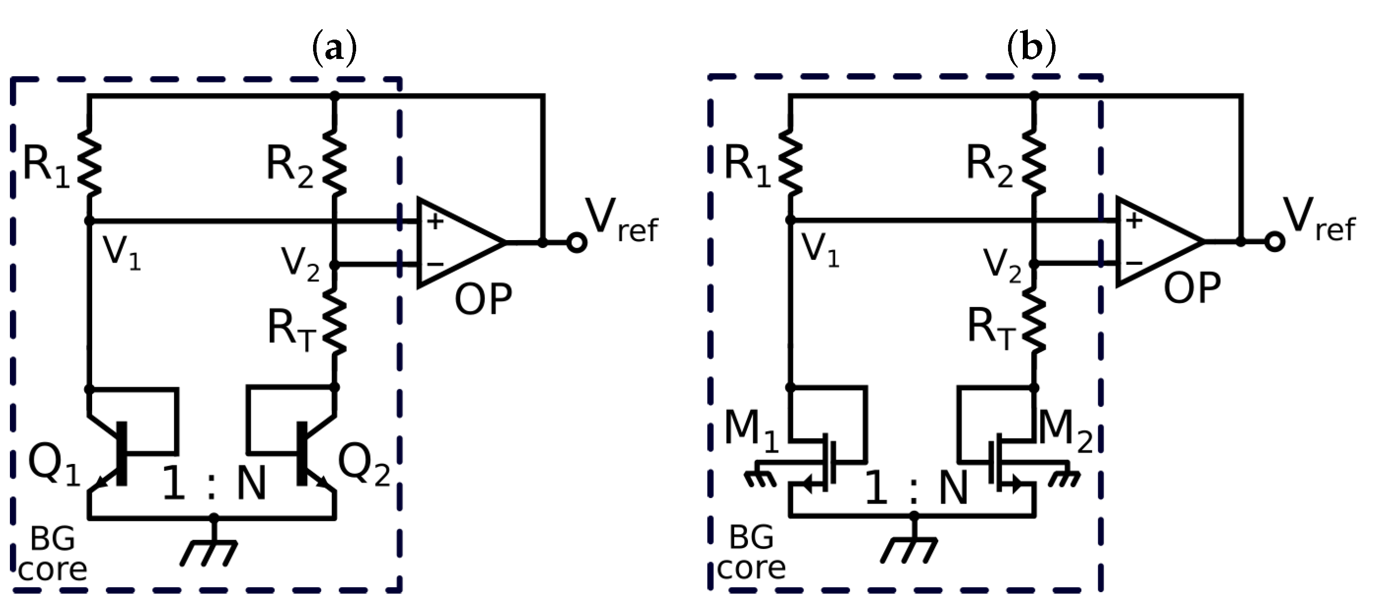
Figure 1a shows the Kujik BG BJT-based core [15], where due to the virtual short-circuit at the amplifier input, resulting in the following ratio of collector currents: . The reference voltage , in the case of (i.e., ), is:
where is the equivalent thermal voltage (k is the Boltzmann constant, T the absolute temperature, and q the electron charge) and N is simply the ratio of the emitter areas of and . A proper sizing of the resistive ratio allows the temperature derivative compensation of at a target temperature, for instance room temperature ( °C), obtaining the typical value of the reference voltage, close to 1.22 V, which practically sets the minimum supply voltage to around 1.4 V.
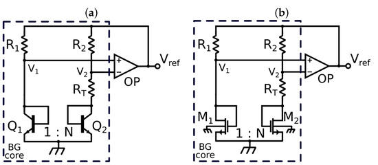
Figure 1.
Schematic view of (a) the bandgap reference voltage proposed in [15] and (b) its all-MOSFET version.
2.1. MOSFET-Based Voltage Reference
In order to reduce the required supply voltage, the two BJTs in the Kujik BG core can be replaced with MOSFETs biased in weak inversion, obtaining the circuit in Figure 1b. The drain current of a MOSFET in weak inversion can be expressed as [37]:
where is the threshold voltage, and are the drain–source and the source–body voltages, respectively, is the transistor-specific current [38], n is the slope factor, is the carrier mobility, is the gate oxide capacitance per unit area, and is the aspect ratio. By simple calculations, the reference voltage of the BG core in Figure 1b is:
where N is the ratio of the and aspect ratios, i.e., . The PTAT term is obtained by calculating and by means of Equation (2), where we supposed that both and work in the saturation region ().
We now briefly evaluate the temperature derivative of around , verifying its role in the CTAT term. Deriving the expression of from Equation (2) and considering the expression of the drain current :
where is the threshold voltage temperature derivative that we approximated as a temperature-independent term, is the overdrive voltage, is the TCR of the resistors, and is the exponent of the temperature dependence of the electron mobility : . The parameter is negative and typically represents the dominant contribution in Equation (4), making the CTAT component, as anticipated.
Following the typical approach of nulling the temperature derivative of for , we obtained the proper value of that allows the first-order temperature compensation of the PTAT and the CTAT terms. Then, with simple calculations, the reference voltage at can be written as:
It is worth mentioning that the reference voltage at does not depend on device bias, provided that work in the weak inversion and saturation region. Assuming the parameter values from the device models of the technology used in this work (standard 0.18 m CMOS process) and an overdrive voltage equal to 0 V, mV/K and V. With typical threshold voltages around 0.4 V, we obtained a reference voltage around 0.6 V. Considering that the margin of the Operational Amplifier (OP) output voltage to is, in the best case, equal to a saturation voltage , a minimum supply voltage of around 0.7 V can be estimated.
In order to scale down the reference voltage, it is possible to choose Low-Threshold-Voltage (LVT) or Zero-Threshold-Voltage (ZVT) devices, which are available in many current CMOS processes. However, we must guarantee the saturation region for , which are diode-connected and have . In weak inversion, the saturation voltage is around . Regular MOSFET devices typically show , and then, the saturation condition is ensured even when overdrive voltages are close to zero or negative. On the other hand, the threshold voltage of LVT devices can be on the order of the saturation voltage, so that are biased at the boundary of the triode region and the effects of and cannot be neglected any more. Consequently, could be no longer PTAT in the whole temperature range of interest. When cannot be neglected in Equation (2), an analytical solution cannot be found.
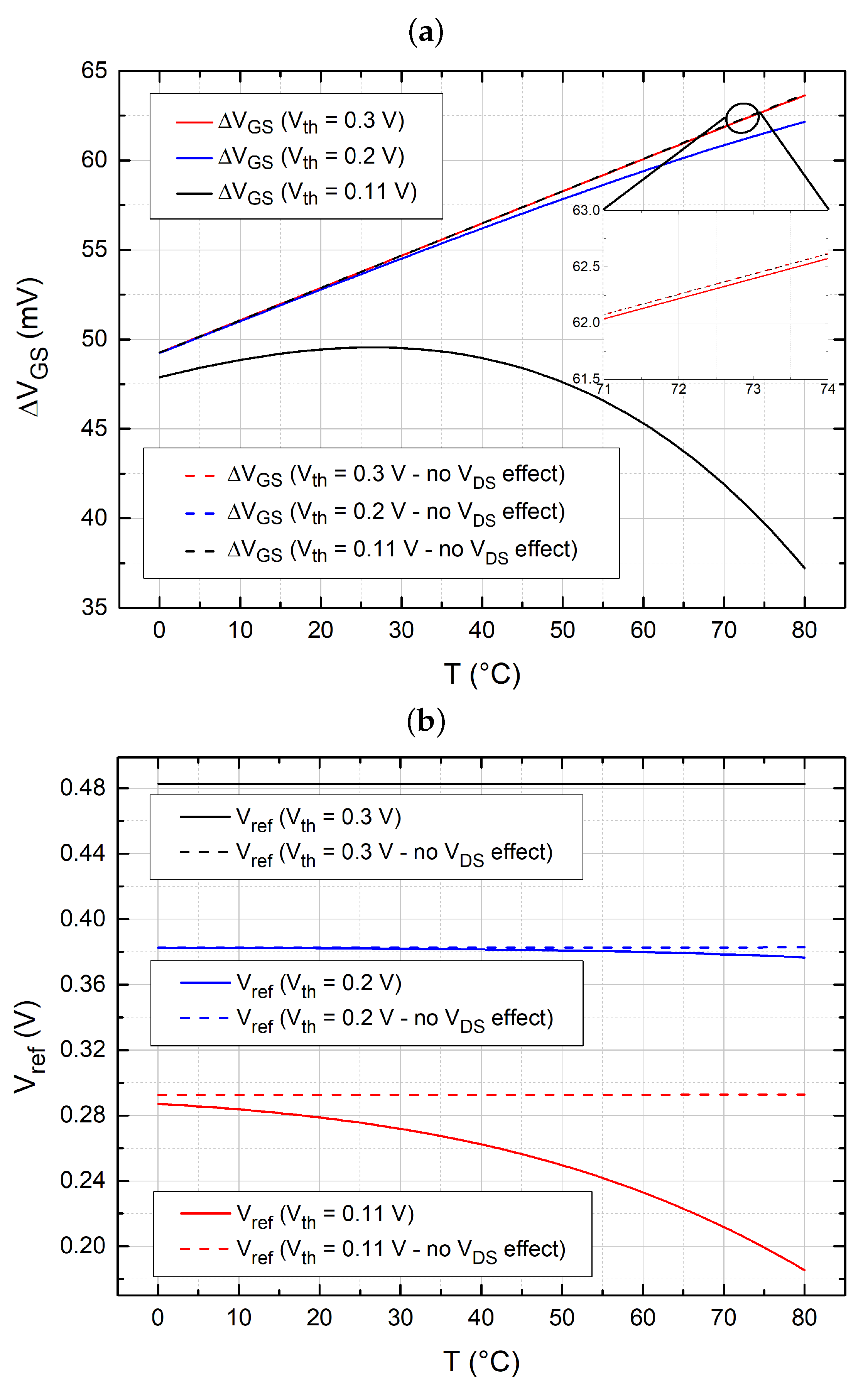
For this reason, we developed a numerical simulator, written using the Scipy scientific modules of the Python language, to solve the network of the BG core depicted in Figure 1b and to find and in a temperature range from 0 °C to 80 °C. The drain currents of were modeled according to Equation (2), tuned with the electrical parameters of a commercial 0.18 m CMOS process. In order to highlight the role played by , we compared the results of simulations performed with and without the -dependent term of Equation (2). In the rest of the paper, we refer to the solution obtained neglecting the as the ideal case. OP was considered ideal with an infinite gain, thus ensuring the virtual short-circuit . was sized to fix the MOSFET drain currents (here, around 200 nA), while was sized to obtain the first-order temperature compensation of the PTAT and the CTAT terms at °C in the ideal case. and were chosen as large as possible to guarantee the weak inversion biasing of both and . The N factor is typically in the range from 2 (minimum area occupation) to 8 (compact common-centroid layouts). We adopted an intermediate value , but the following results did not vary significantly with this parameter, once R and were properly resized accordingly. Finally, three different values of were considered in the simulations: 0.11, 0.2, 0.3 V.
Figure 2a shows the temperature behavior of for different (simply expressed as in the plot legends). The dashed curves represent the ideal : notice that the curves are practically coincident, showing that there is no influence from the threshold voltage, in agreement with Equation (3). On the other hand, the curves obtained by taking into account also the effect strongly depend on . For V, the effect of is almost negligible, as shown also in the inset of Figure 2a. For a lower value of (0.2 V), differs from the ideal curve especially for large temperatures, while for even lower values of (e.g., 0.11 V), the temperature behavior of is not PTAT any more in the whole temperature range. It was not possible to repeat the simulations for V (corresponding to typical LVT or ZVT devices), because (and consequently ) became negative for a certain range of temperatures and the numerical solver failed to find the correct solution of the equation set. Figure 2b shows the temperature behavior of for the same values as in Figure 2a. Failure in obtaining a correct PTAT voltage for low is clearly reflected in the temperature stability of . A significant deviation from the ideal case can be observed for V, while for V, the effect of completely disrupts the temperature stabilization mechanism. For V, instead, the temperature behavior is practically the same as in the ideal case; however, it is worth noting that the value of the obtained reference voltage is close to 0.5 V. Considering the minimum overhead required by the amplifier, this results in a reasonable minimum value of about 0.6 V. In the next section, we present a new BG topology where the use of LVT or ZVT devices did not incur the above-mentioned issue, thus allowing further scaling of the minimum supply voltage.
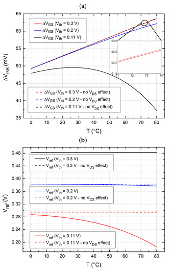
Figure 2.
Temperature behavior of (a) and (b) in the BG core of Figure 1b, for different values of , considering or neglecting the effect on the drain current.
2.2. Proposed BG Core
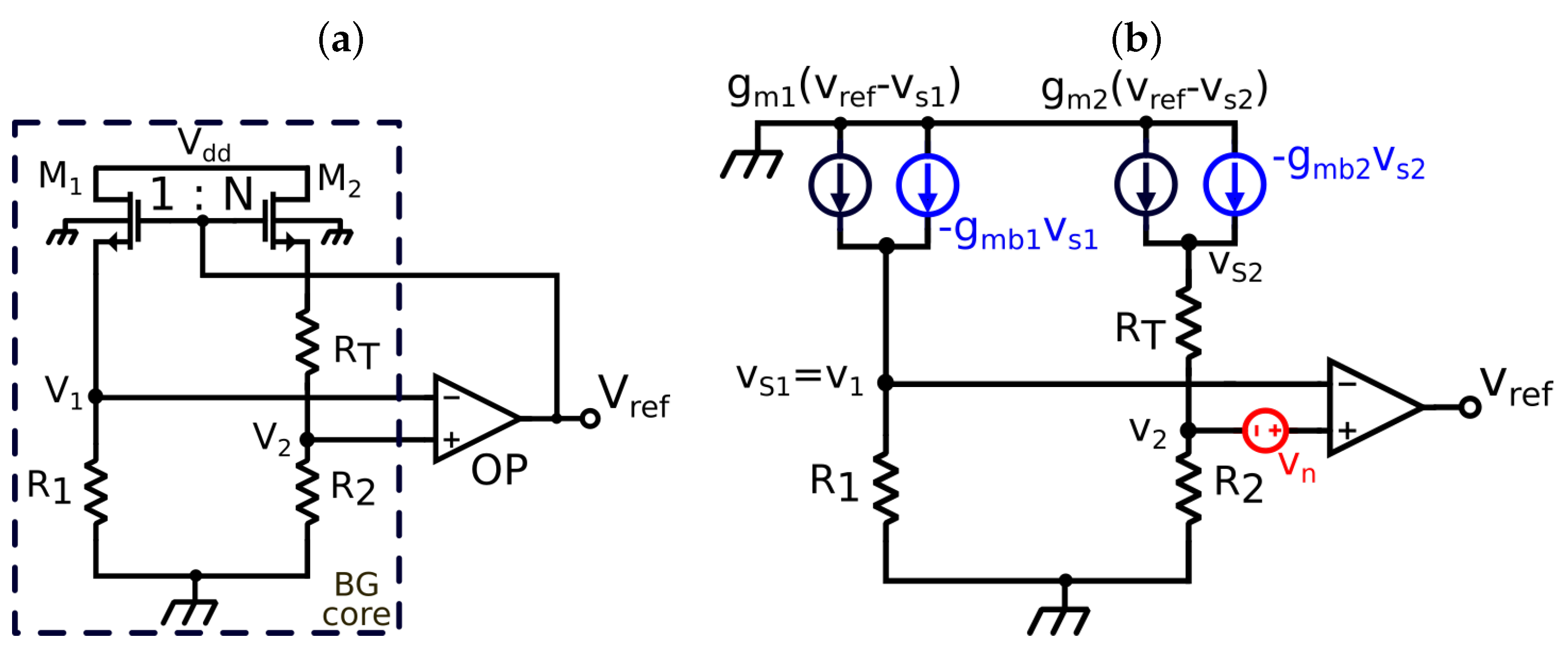
Figure 3a shows the proposed BG core, where the diode connections of were removed and the drain terminals were connected to the supply voltage, while the resistive network made by , , and was shifted to the source side. In this way, can be larger than and does not suffer from the small values assumed by the latter in LVT and ZVT devices. It is straightforward to verify that the working principle of the proposed core is identical to that of Figure 1b, with the only difference that of is not zero. Thus, the reference voltage is then:
which differs from Equation (3) only for the absence of the factor n in the PTAT term. In a triple-well process (or p-well), a source–body connection would be allowed, making the of the circuits in Figure 1b and Figure 3a perfectly equivalent. This condition is clearly not essential, since the sum of a PTAT and a CTAT term is present in the expression of given in Equation (6). More interestingly, it is possible to demonstrate that, imposing an ratio that nulls the temperature derivative at , the expression of the reference voltage of the proposed BG core at is the same as Equation (5) regardless of the presence of a body–source connection. Thus, V, as in the case of the standard core of Figure 1b. With the proposed core, the value can be lowered by means of employing LVT or ZVT devices, without incurring the problems that affect the standard core. The limiting condition on the minimum supply voltage is given by entering the triode region. The minimum value is determined by the following condition:

Figure 3.
Schematic view of (a) the proposed bandgap reference voltage and (b) its equivalent small signal circuit.
Expanding the term by simple calculations based on the analysis performed above, the minimum at can be written as:
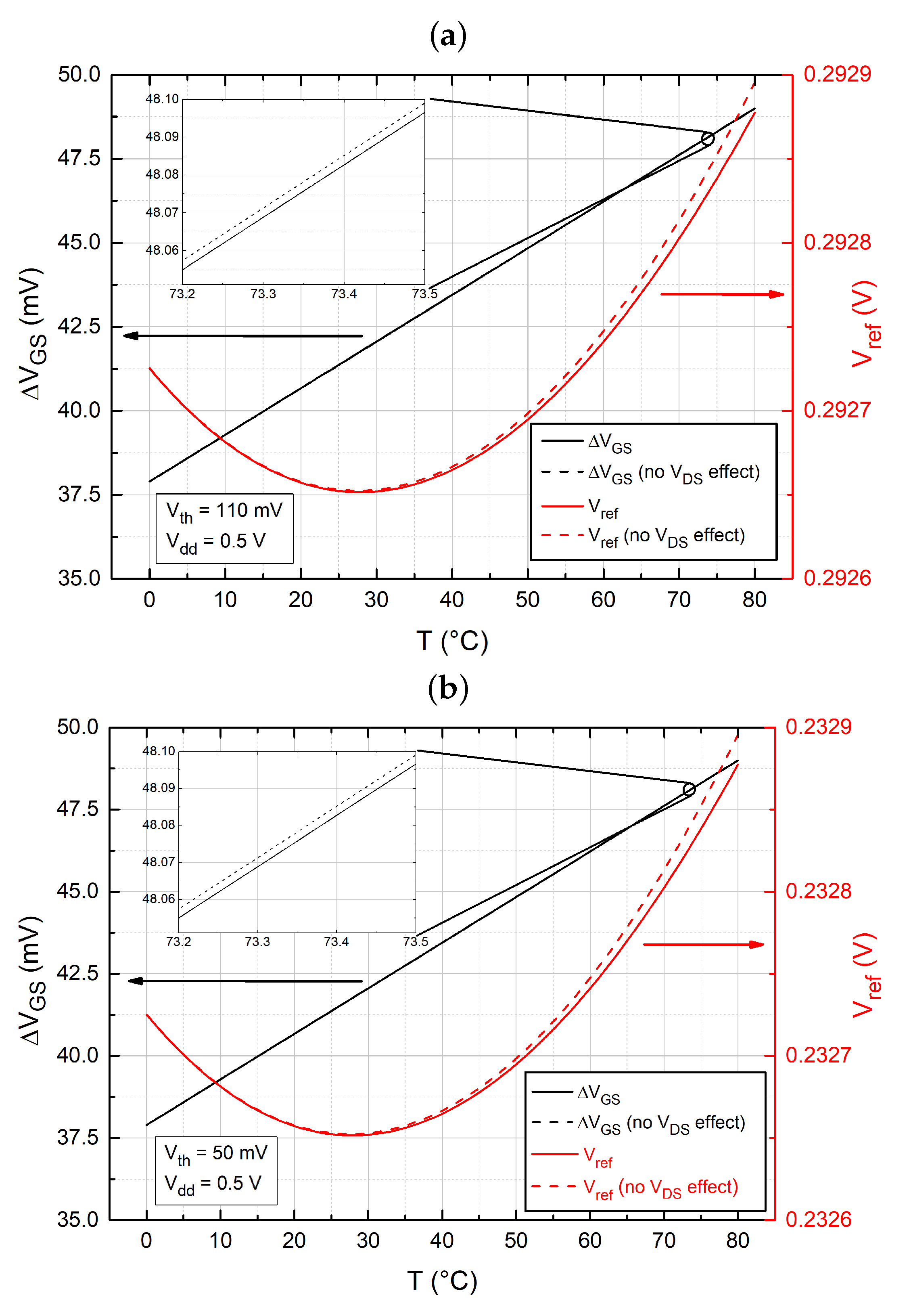
In order to verify the correct behavior of the proposed core and find a more accurate value of , we performed numerical simulations also on the proposed BG core. The physical and geometrical parameters used in the simulation program were the same as the ones used for the standard core, except for , which was slightly different to compensate the different slope of the PTAT term.
Figure 4a shows the temperature behavior of and in the case of and with V and V. As in the case of the standard core, simulations were performed with and without the -dependent term in Equation (2). Differently from Figure 2a, is minimally affected by the effect, maintaining an excellent linear dependence from the temperature. Furthermore, also the temperature behavior of is very close to the ideal one. In Figure 4b, we performed the same simulations, but considering mV, which is close to the actual value of the threshold voltage of an LVT device in the adopted technology. The temperature behavior for both and is still quite close to the ideal case, but the absolute value of is obviously lower.
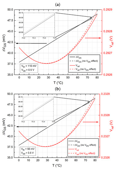
Figure 4.
Temperature behavior of and in the BG core of Figure 3a, for V, considering or neglecting the effect on the drain current, for mV (a) and mV (b).
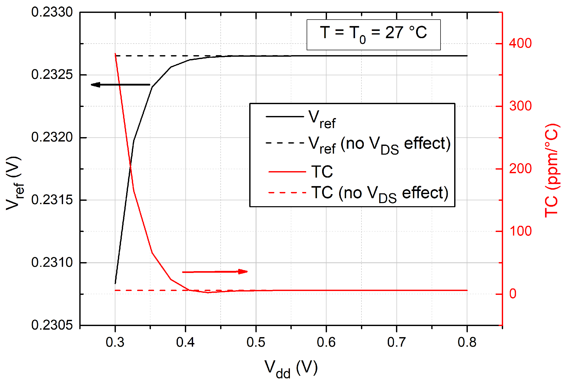
Figure 5 shows the variations of and the temperature coefficient (TC) as a function of the supply voltage. The temperature coefficient is defined as: , where and are the maximum and the minimum values of over the investigated temperature interval and °C is the total temperature excursion. In the case of neglecting the effect (dashed curves), no dependence on the supply voltage is present. Actually, appreciable variations of and TC are present only for values of lower than 0.4 V. This value is larger than the estimate given in Equation (8). This discrepancy derives from considering an abrupt transition between saturation and triode region. In practice, the effects start being non-negligible for values higher than the value (100 mV) used in Equation (8).
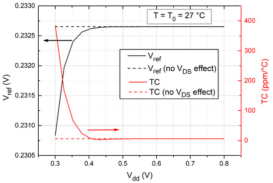
Figure 5.
Supply voltage dependence of (at ) and the Temperature Coefficient (TC), considering or neglecting the effect on the drain current.
2.3. Offset and Noise Contribution of the Amplifier
Bandgap topologies that employ an operational amplifier to ensure equal currents in the two branches of the core necessarily suffer from the effect of offset and noise introduced by the op amp [35]. The Referred-To-Input (RTI) error voltage of OP, indicated in Figure 3b as , gives a contribution to the reference voltage equal to :
where is a small signal transfer function defined as follows:
From the equivalent small signal circuit of the proposed BG core depicted in Figure 3b, considering that , it is straightforward to evaluate :
Because of the design choice and consequently , the transconductance of biased in weak inversion is equal to . By nulling the temperature derivative of expressed in Equation (6) around , we derive . Finally, we can express as:
Considering a typical range of N from 2 to 8, varies from 0.05 to 0.15. As a result, according to Equation (9), can be from 7- to 20-times . For this reason, the input voltage noise and offset of the amplifier can significantly degrade the reference voltage accuracy. As shown in the next section, the proposed core was combined with an amplifier performing Correlated Double Sampling (CDS) to reduce its offset and low-frequency noise.
3. Prototype Design
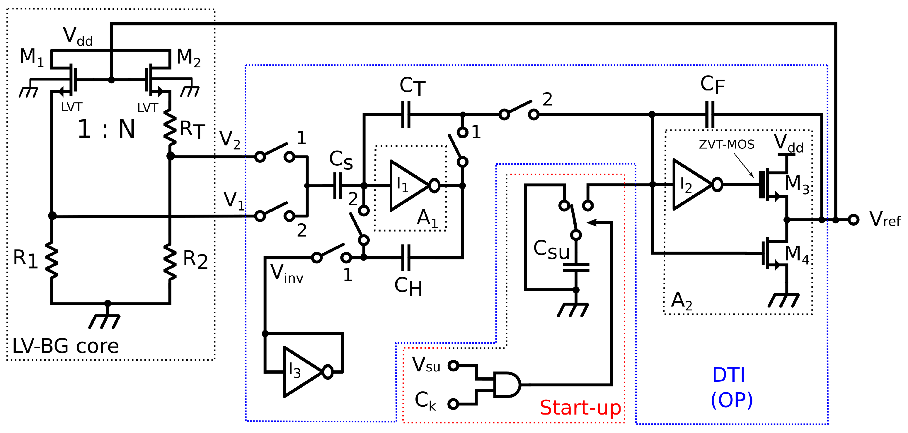
The proposed LV-VR, shown in Figure 6, was implemented using a 0.18 m CMOS process from UMC. The LV-BG core was the same as just described in the previous section where transistors are LVT devices, having threshold voltages () lower than 100 mV. The amplifier OP was replaced by a Discrete Time (DT) Switched Capacitor (SC) integrator (DTI), enclosed inside the blue dotted polygon in Figure 6. The integrator was presented for the first time in [34] and was selected for the proposed LV-VR since it offers the following unique combination of properties: (i) it operates CDS, reducing the input-referred offset voltage and low frequency noise; (ii) its output voltage is valid across the whole clock cycle, making it equivalent to a continuous-time integrator; (iii) it ideally does not draw current from the inputs as soon as the virtual short-circuit is established; (iv) it provides a high DC gain. The integrator is formed by two stages, built around amplifiers and . In turn, and are based on gain stages ( and ), consisting of standard CMOS inverters. In , the inverter is followed by a source-follower stage (devices ), introduced to allow driving resistive loads with reduced gain loss. In order to maintain an acceptable output range, a ZVT device (native n-MOSFET) was used for . The circuit operates with a two-phase clock. Switches are labeled with numbers that indicate the clock phase where they are closed (on state). The detailed operating principle of the SC integrator was analyzed in [34]. Briefly, in the transition between Phase 2 to Phase 1, a charge proportional to the input differential voltage () is injected from capacitor into capacitor . In the transition between Phase 1 and the following Phase 2, this charge is transferred to , which produces a voltage increment equal to , proving that the circuit operates as a DT integrator. It can be easily verified that the voltages at the input of and contribute to all charge transfers only in the form of the differences of samples taken at different instants of the clock cycle. This proves that CDS is actually applied to and input offset and low-frequency noise voltages. Capacitor is used to maintain negative feedback in Phase 2, when is transferring charge to . The use of instead of a direct input–output connection reduces the output swing of the output voltage across phase transitions, increasing the equivalent DC gain of the integrator. For this mechanism to be effective, in Phase 1, must be connected to a voltage as close as possible to the closed-loop input voltage. This voltage, indicated with , is produced by inverter closed in unity gain configuration. The DC gain of the integrator can be shown to be in the order of . As a result, even with the typically small gains of inverter-like amplifiers (order of tens, at ultralow supply voltages), DC gains of several thousands are guaranteed using the adopted two-stage integrator.
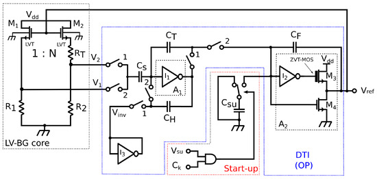
Figure 6.
Schematic view of the proposed LV-VR.
3.1. Start-Up Circuit
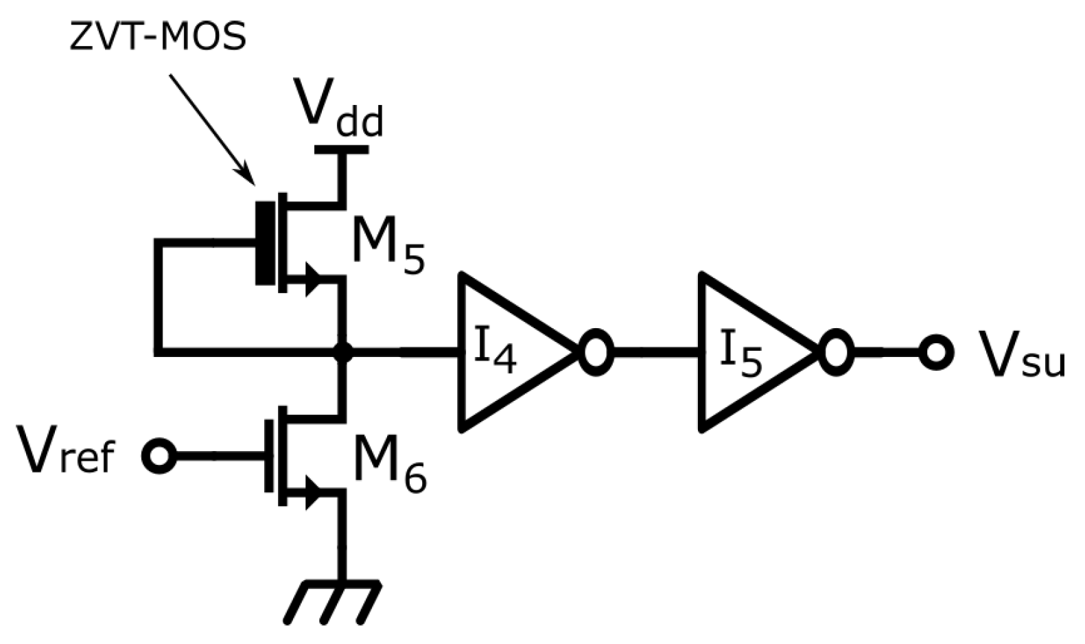
As in traditional bandgap-like structures, the proposed circuit suffers from the presence of an unwanted all-zero stable solution. To prevent the circuit from being trapped, a start-up architecture is mandatory. The start-up circuit adopted in this work is shown in the red dashed box in Figure 6: is the clock signal, while is the output voltage of the low-voltage comparator shown in Figure 7. The comparator is composed by a cascade of three inverters: the first one, and , sets the threshold voltage, and the other two inverters make the transition sharper. The threshold voltage is reached when the input voltage of the comparator (i.e., ) is such that the current in equals the constant current provided by . By proper sizing of and , the threshold voltage was set to a value slightly lower than the steady-state value of , even considering the spread due to the process variations. When voltage is lower than the comparator threshold voltage, the charge pump formed by capacitor pumps charges into , allowing to increase to a voltage large enough to enable the circuit to start its autonomous evolution towards the correct steady-state solution. Since the steady-state value of is larger than the comparator threshold voltage, the start-up circuit is normally powered off.
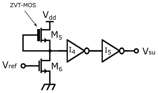
Figure 7.
Schematic view of the auxiliary LV-comparator.
3.2. Device Sizing
As shown in Figure 6, the proposed prototype is formed by two main blocks, namely the bandgap core and the amplifier (SC integrator). The procedure used to design the core is very simple, and this is a clear advantage of Kujik-like solutions. and are LVT devices, characterized by a threshold voltage around 50 mV. The value of N, which is not critical, sets the voltage across resistor (PTAT voltage). In turn, sets the bias current through and , i.e., the power consumption of the core. Once the magnitude of the current is established, ’s aspect ratio must be chosen large enough to keep the MOSFET in weak inversion. This step sets ’s overdrive voltage, which is not critical, since it does not affect the value of , according to Equation (5). Finally, the ratio is set to the value that nulls the derivative of with respect to temperature. This last step can be simply accomplished by means of a single parametric sweep, performed using the electrical simulator. We chose a value of N equal to 5, which was obtained by connecting five replicas in parallel to form . In practice, this corresponded to setting the multiplicity factor (m) of to 5. The value of was chosen to set the core current consumption to a few hundred nA. Clearly, larger resistance values can be adopted to reduce the current consumption, at the cost of a larger area occupation. As far as the SC integrator is concerned, transistors and are ZVT MOSFETs, and the remaining transistors are Regular Threshold Voltage (RVT) devices. Complementary transmission gates employing regular threshold devices were used for all switches.
Table 1 and Table 2 summarize the sizes of the active and passive components, respectively. As far as passive components are concerned, resistors , , and are high-resistivity polysilicon resistors, and all capacitors are metal–insulator–metal devices.

Table 1.
Sizing of LV-VR transistors.
Table 2.
Sizing of LV-VR passive components.
4. Results
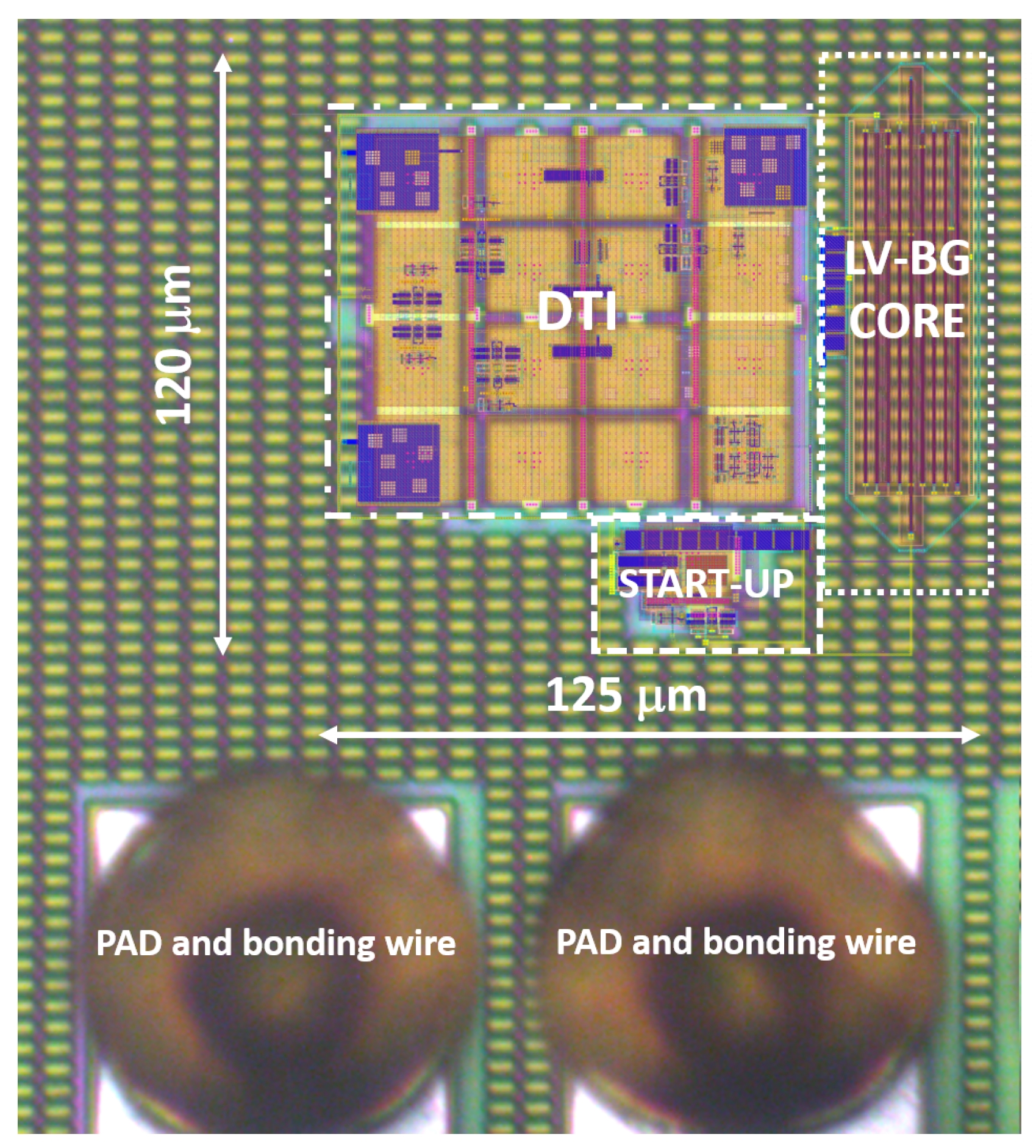
The proposed LV-VR was designed with the Cadence Virtuoso Platform for Custom IC design, electrically verified by means of the Spectre simulator and fabricated with the UMC 0.18 CMOS process. An optical micrograph of the proposed voltage reference is shown in Figure 8, where the layout is superimposed on the picture. The total area consumption was close to 0.015 mm2. All tests were performed with = 0.5 V, T = 27 °C, and = 100 kHz, unless otherwise specified.
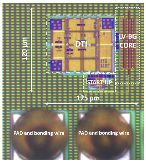
Figure 8.
Micrograph of the proposed voltage reference with the layout aligned and superimposed in order to show the devices and interconnections that would be otherwise hidden below the planarization dummies. The dimensions and the main blocks are indicated.
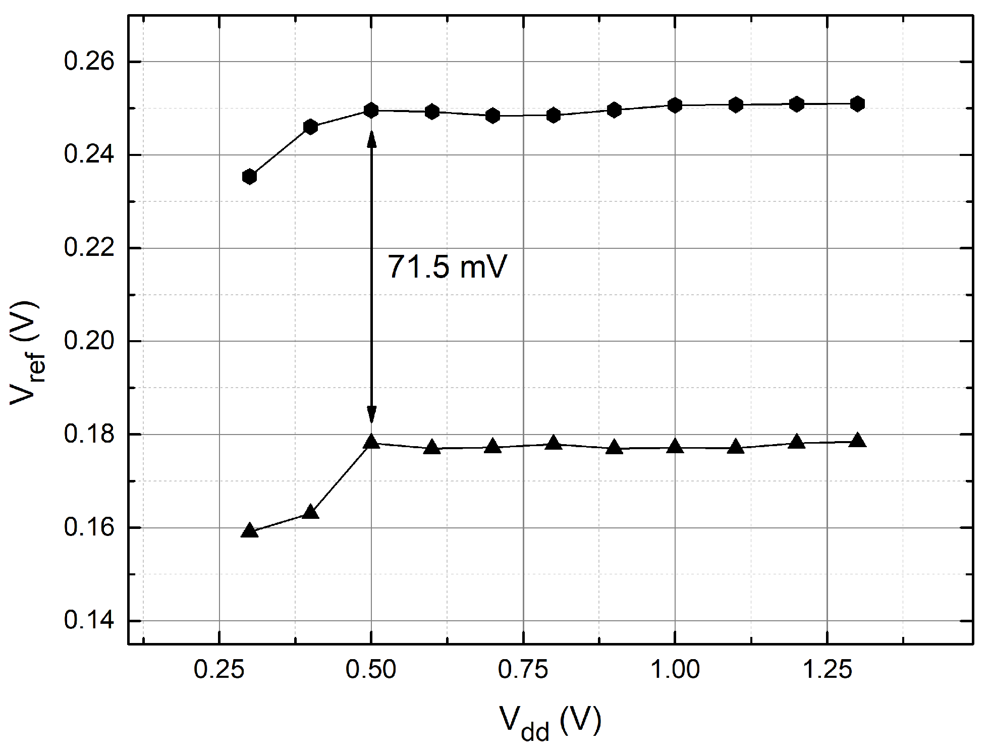
The dependence of on the supply voltage was measured over a set of ten chips. Figure 9 shows the highest (dots) and the lowest (triangle) vs. characteristics. The spread between the two curves is 71.5 mV. Since the main contribution of the reference voltage is represented by the threshold voltage, it can be argued that this uncertainty is mainly due to the spread. Corner process simulations confirmed that the variation of the and threshold voltages was actually close to the reference voltage spread. The circuit started working properly with = 0.5 V and in the supply voltage range from 0.5 V to 1.3 V the variation was close to 2 mV for both characteristics. Note that the lower limit was higher than the 0.4 V prediction derived from the numerical simulations of Figure 5. This could be due to additional constraints on imposed by the SC integrator.
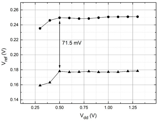
Figure 9.
Measured output voltage, , as a function of the power supply at room temperature.
The temperature dependence is shown in Figure 10 for a sample that exhibits an intermediate value with respect to the extremes shown in Figure 9. Measurements were performed using a Peltier-cell cryostat sweeping the temperature in the range 10 °C to 80 °C. A maximum variation of 6.7 mV can be observed in the whole temperature range. If we focus on the temperature range generally considered for wearable applications [39] (i.e., from 10 °C up to 50 °C), the variation was close to 1 mV, with an average TC of 45 ppm/°C.
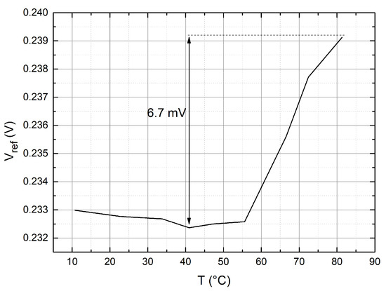
Figure 10.
Measured temperature dependence of the output voltage in the range 10 °C to 80 °C.
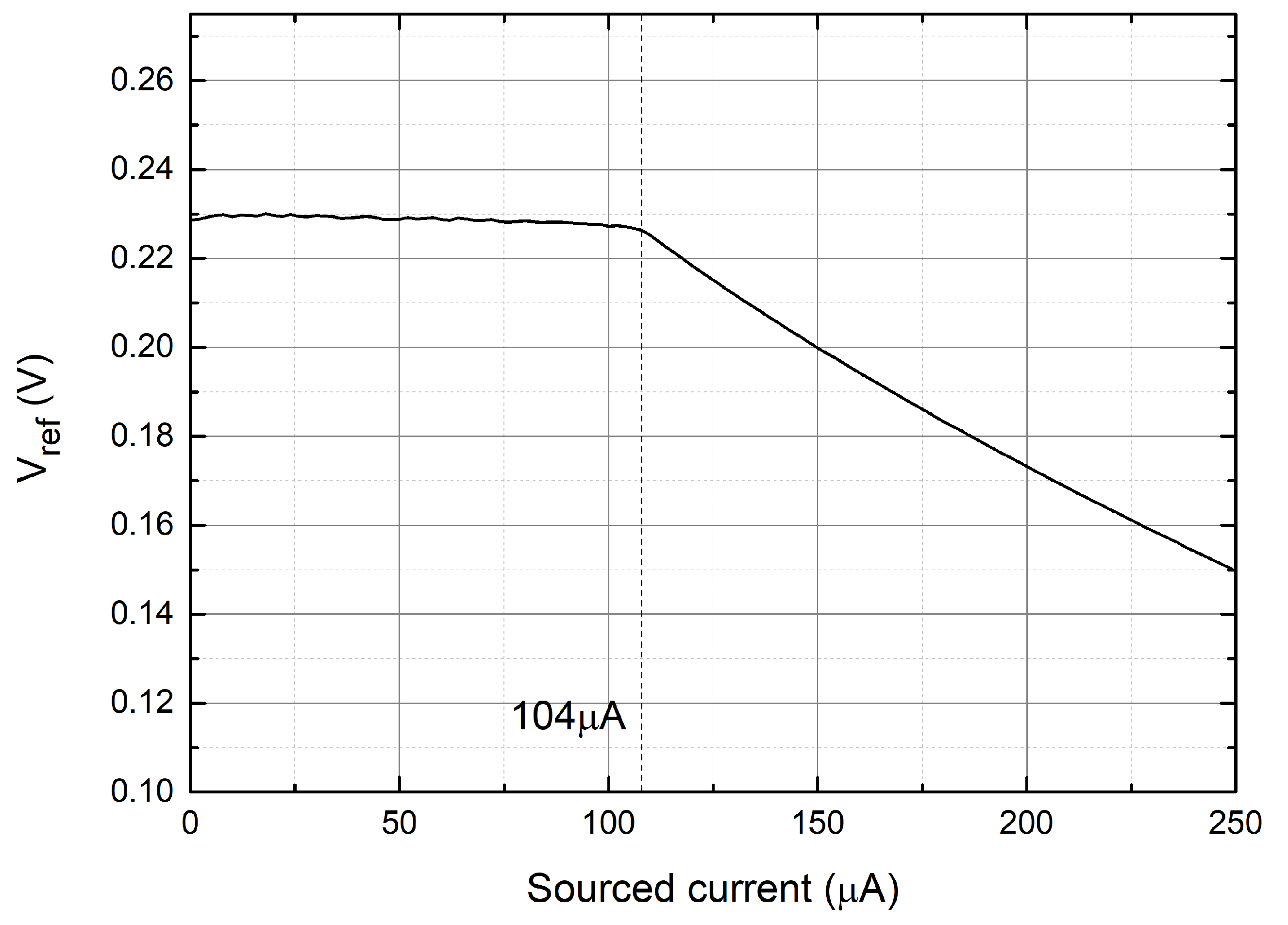
In Figure 11, the output reference voltage is plotted as a function of the output current. It is possible to observe that undergoes very small variations for sourced current up to 104A. The bias current of the proposed bandgap was around 630 nA, and thus, the maximum sourced current was 165-times larger than the bias one.
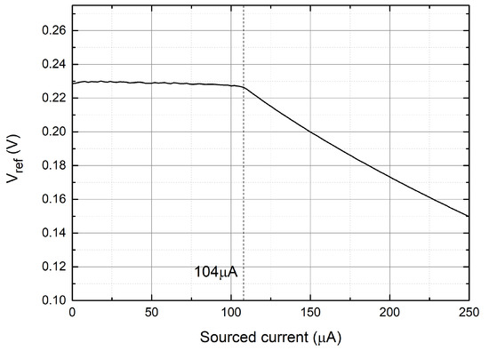
Figure 11.
Measured output reference voltage vs. sourced output current.
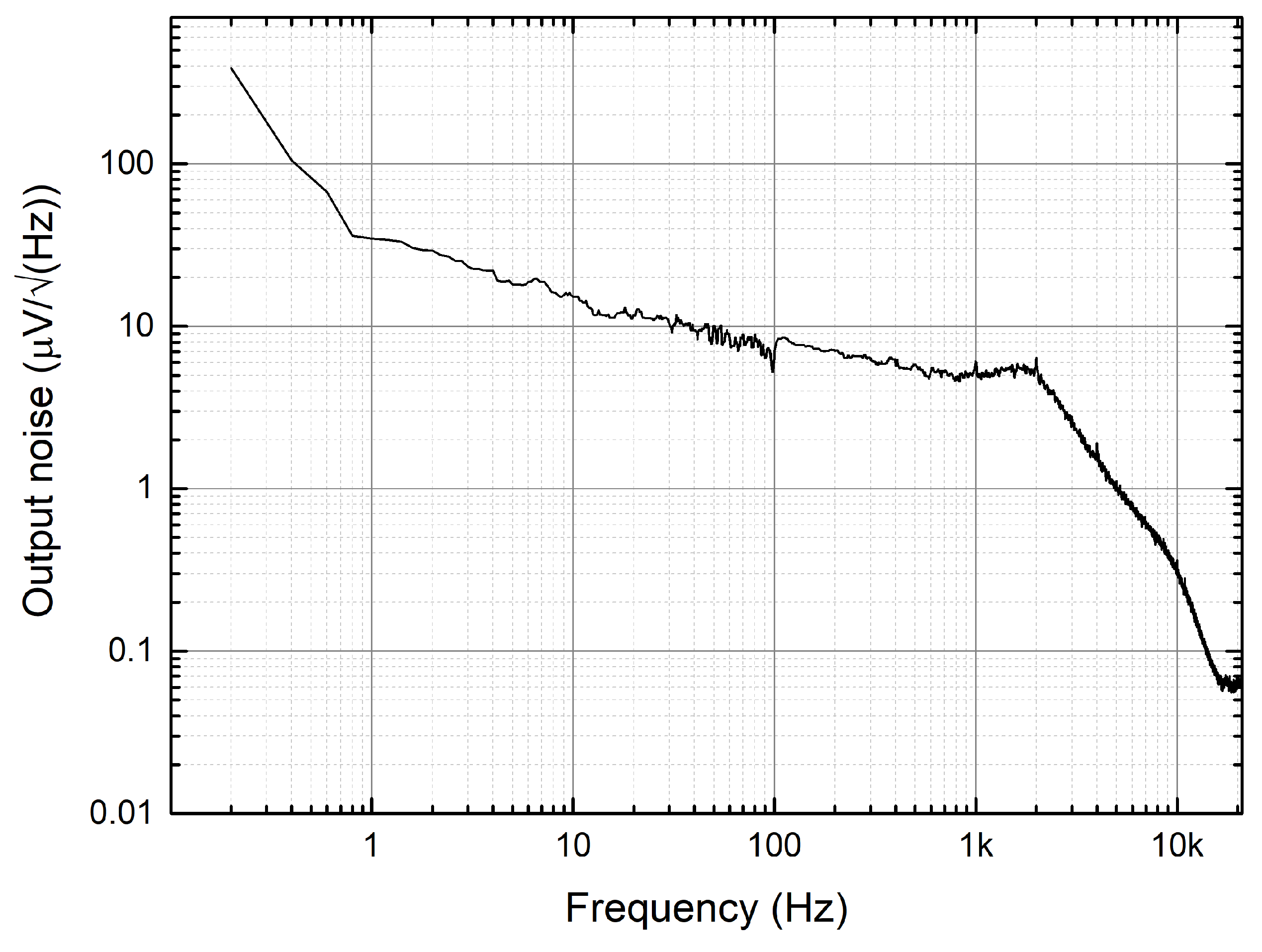
Finally, the unfiltered output noise density is depicted in Figure 12. The noise density decrease for frequencies higher than 2 kHz was due to the intrinsic DT transfer function of the feedback loop [35]. A typical flicker noise component can be observed at low frequencies. This can be ascribed to contributions from , which differently from the input noise of the amplifier, are not subjected to correlated-double sampling. The root-mean-squared voltage noise in the bandwidth from 0.2 Hz to 10 kHz was around 330 .
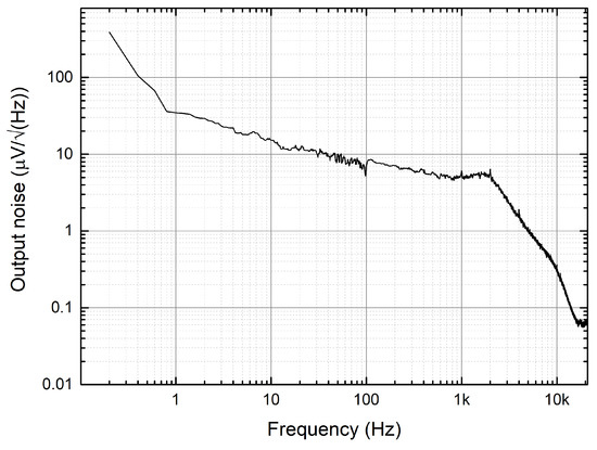
Figure 12.
Output noise spectral density. Noise density in the flat region is indicated.
The performance of the VR prototype described in this paper is summarized in Table 3, where the data extracted by recent works on Sub-1 V references are also reported. The proposed solution is lines up with most of the state-of-the-art designs included in the comparison. A point of weakness is represented by the power consumption, which could be simply overcome by scaling up the values of all resistors by the same factor, obviously at the cost of increased area occupation. Furthermore, it should be noted that, differently from the proposed circuit, all the VRs reported in Table 3 have no capability of sourcing significant output currents, with the exception of Reference [22]. The impressively low supply voltage reported in [33] was obtained by applying active body biasing to n-MOSFETs, which is not compatible with inexpensive n-well CMOS processes. The other work in the table that exhibits a supply voltage below 0.3 V [29] actually used a charge pump to double the value of , providing the headroom required to bias a current mode bandgap core.
Table 3.
Performance summary and comparison of state-of-the-art LV VRs.
5. Conclusions
It was shown that direct replacement of the BJTs with low-threshold MOSFETs in the popular Kuijk bandgap core [15] is not a viable solution to obtain VRs compatible with ultralow supply voltages. The weakness was found to be the diode connection of the MOSFETs, which results in an insufficient when the devices are biased in the deep subthreshold region. The main effect is a failure in the PTAT voltage/current generation, which occurs independently of the value. It is worth noting that the observed problem should affect in the same way different architectures where a mesh of diode-connected MOSFETs is used to obtain a PTAT current [28,29]. The proposed improvement was demonstrated to be suitable for the design of Kuijk-like cores with very low-threshold-voltage MOSFETs. The principle, which was illustrated with analytical arguments, was also supported by experimental results obtained from the proposed prototype, designed using a standard CMOS n-well technology. Another merit of the prototype was the use of a recently introduced SC integrator, which, differently from other alternative designs operating CDS for offset and noise reduction, produced a really time-continuous output, which was valid across the whole clock cycle. Thanks to the inverter-like implementation of the integrator, the correct operation of the prototype was enabled down to 0.5 V. Note that the described prototype represents only one of the possible implementations of voltage references based on the proposed core. Different solutions where the resistor values are increased to reduce power consumption or alternative amplifier topologies are employed can be envisioned.
Author Contributions
All authors participated in the conceptualization and methodology of this work. Data curation, A.R. and A.C.; writing—original draft preparation, A.R., A.C. and P.B.; writing—review and editing: M.P. and P.B. All authors read and agreed to the published version of the manuscript.
Funding
This research was partially supported by the Italian Ministry of Education and Research (MIUR) in the framework of the CrossLab project (Departments of Excellence).
Conflicts of Interest
The authors declare no conflict of interest. The funders had no role in the design of the study; in the collection, analyses, or interpretation of data; in the writing of the manuscript; nor in the decision to publish the results.
References
- Qiu, S.; Wang, Z.; Zhao, H.; Hu, H. Using Distributed Wearable Sensors to Measure and Evaluate Human Lower Limb Motions. IEEE Trans. Instrum. Meas. 2016, 65, 939–950. [Google Scholar] [CrossRef] [Green Version]
- Selvam, A.P.; Muthukumar, S.; Kamakoti, V.; Prasad, S. A wearable biochemical sensor for monitoring alcohol consumption lifestyle through Ethyl glucuronide (EtG) detection in human sweat. Sci. Rep. 2016, 6, 1–11. [Google Scholar] [CrossRef]
- Saraereh, O.A.; Alsaraira, A.; Khan, I.; Choi, B.J. A Hybrid Energy Harvesting Design for On-Body Internet-of-Things (IoT) Networks. Sensors 2020, 20, 407. [Google Scholar] [CrossRef] [PubMed] [Green Version]
- Lo Presti, D.; Carnevale, A.; D’Abbraccio, J.; Massari, L.; Massaroni, C.; Sabbadini, R.; Zaltieri, M.; Di Tocco, J.; Bravi, M.; Miccinilli, S.; et al. A Multi-Parametric Wearable System to Monitor Neck Movements and Respiratory Frequency of Computer Workers. Sensors 2020, 20, 536. [Google Scholar] [CrossRef] [PubMed] [Green Version]
- Bariya, M.; Nyein, H.Y.Y.; Javey, A. Wearable sweat sensors. Nat. Electron. 2018, 1, 160–171. [Google Scholar] [CrossRef]
- Dei, M.; Aymerich, J.; Piotto, M.; Bruschi, P.; del Campo, F.J.; Serra-Graells, F. CMOS Interfaces for Internet-of-Wearables Electrochemical Sensors: Trends and Challenges. Electronics 2019, 8, 150. [Google Scholar] [CrossRef] [Green Version]
- Oktavius, A.K.; Gu, Q.; Wihardjo, N.; Winata, O.; Sunanto, S.W.; Li, J.; Gao, P. Fully-Conformable Porous Polyethylene Nanofilm Sweat Sensor for Sports Fatigue. IEEE Sens. J. 2021, 21, 8861–8867. [Google Scholar] [CrossRef]
- Wang, H.; Wang, G.; Ling, Y.; Qian, F.; Song, Y.; Lu, X.; Chen, S.; Tong, Y.; Li, Y. High power density microbial fuel cell with flexible 3D graphene–nickel foam as anode. Nanoscale 2013, 5, 10283–10290. [Google Scholar] [CrossRef]
- Talkhooncheh, A.H.; Yu, Y.; Agarwal, A.; Kuo, W.W.T.; Chen, K.C.; Wang, M.; Hoskuldsdottir, G.; Gao, W.; Emami, A. A Biofuel-Cell-Based Energy Harvester With 86% Peak Efficiency and 0.25-V Minimum Input Voltage Using Source-Adaptive MPPT. IEEE J. Solid-State Circuits 2021, 56, 715–728. [Google Scholar] [CrossRef]
- Tanwar, A.; Lal, S.; Razeeb, K.M. Structural Design Optimization of Micro-Thermoelectric Generator for Wearable Biomedical Devices. Energies 2021, 14, 2339. [Google Scholar] [CrossRef]
- Khan, S.; Kim, J.; Roh, K.; Park, G.; Kim, W. High power density of radiative-cooled compact thermoelectric generator based on body heat harvesting. Nano Energy 2021, 87, 106180. [Google Scholar] [CrossRef]
- Proto, A.; Vondrak, J.; Schmidt, M.; Kubicek, J.; Gorjani, O.M.; Havlik, J.; Penhaker, M. A Flexible Thermoelectric Generator Worn on the Leg to Harvest Body Heat Energy and to Recognize Motor Activities: A Preliminary Study. IEEE Access 2021, 9, 20878–20892. [Google Scholar] [CrossRef]
- Alioto, M. Enabling the Internet of Things: From Integrated Circuits to Integrated Systems; Springer: New York, NY, USA, 2017. [Google Scholar] [CrossRef]
- Widlar, R. New developments in IC voltage regulators. IEEE J. Solid-State Circuits 1971, 6, 2–7. [Google Scholar] [CrossRef] [Green Version]
- Kuijk, K.E. A precision reference voltage source. IEEE J. Solid-State Circuits 1973, 8, 222–226. [Google Scholar] [CrossRef]
- Kok, C.W.; Tam, W.S. CMOS Voltage References: An Analytical and Practical Perspective; John Wiley & Sons: Hoboken, NJ, USA, 2012. [Google Scholar] [CrossRef]
- Ferro, M.; Salerno, F.; Castello, R. A floating CMOS bandgap voltage reference for differential applications. IEEE J. Solid-State Circuits 1989, 24, 690–697. [Google Scholar] [CrossRef]
- Banba, H.; Shiga, H.; Umezawa, A.; Miyaba, T.; Tanzawa, T.; Atsumi, S.; Sakui, K. A CMOS bandgap reference circuit with sub-1-V operation. IEEE J. Solid-State Circuits 1999, 34, 670–674. [Google Scholar] [CrossRef] [Green Version]
- Malcovati, P.; Maloberti, F.; Fiocchi, C.; Pruzzi, M. Curvature-compensated BiCMOS bandgap with 1-V supply voltage. IEEE J. Solid-State Circuits 2001, 36, 1076–1081. [Google Scholar] [CrossRef] [Green Version]
- Boni, A. Op-amps and startup circuits for CMOS bandgap references with near 1-V supply. IEEE J. Solid-State Circuits 2002, 37, 1339–1343. [Google Scholar] [CrossRef] [Green Version]
- Sanborn, K.; Ma, D.; Ivanov, V. A Sub-1-V Low-Noise Bandgap Voltage Reference. IEEE J. Solid-State Circuits 2007, 42, 2466–2481. [Google Scholar] [CrossRef]
- Ivanov, V.; Brederlow, R.; Gerber, J. An Ultra Low Power Bandgap Operational at Supply From 0.75 V. IEEE J. Solid-State Circuits 2012, 47, 1515–1523. [Google Scholar] [CrossRef]
- Chi-Wa, U.; Zeng, W.L.; Law, M.K.; Lam, C.S.; Martins, R.P. A 0.5-V Supply, 36 nW Bandgap Reference With 42 ppm/°C Average Temperature Coefficient Within -40 °C to 120 °C. IEEE Trans. Circuits Syst. I Regul. Pap. 2020, 67, 3656–3669. [Google Scholar] [CrossRef]
- Tzanateas, G.; Salama, C.; Tsividis, Y. A CMOS bandgap voltage reference. IEEE J. Solid-State Circuits 1979, 14, 655–657. [Google Scholar] [CrossRef]
- Vittoz, E.; Neyroud, O. A low-voltage CMOS bandgap reference. IEEE J. Solid-State Circuits 1979, 14, 573–579. [Google Scholar] [CrossRef]
- Giustolisi, G.; Palumbo, G.; Criscione, M.; Cutri, F. A low-voltage low-power voltage reference based on subthreshold MOSFETs. IEEE J. Solid-State Circuits 2003, 38, 151–154. [Google Scholar] [CrossRef]
- Zhuang, H.; Zhu, Z.; Yang, Y. A 19-nW 0.7-V CMOS Voltage Reference with No Amplifiers and No Clock Circuits. IEEE Trans. Circuits Syst. II Express Briefs 2014, 61, 830–834. [Google Scholar] [CrossRef]
- Yang, Y.; Binkley, D.M.; Li, L.; Gu, C.; Li, C. All-CMOS subbandgap reference circuit operating at low supply voltage. In Proceedings of the 2011 IEEE International Symposium of Circuits and Systems (ISCAS), Rio de Janeiro, Brazil, 15–18 May 2011; pp. 893–896. [Google Scholar] [CrossRef]
- Yang, B.D. 250-mV Supply Subthreshold CMOS Voltage Reference Using a Low-Voltage Comparator and a Charge-Pump Circuit. IEEE Trans. Circuits Syst. II Express Briefs 2014, 61, 850–854. [Google Scholar] [CrossRef]
- Blauschild, R.; Tucci, P.; Muller, R.; Meyer, R. A new NMOS temperature-stable voltage reference. IEEE J. Solid-State Circuits 1978, 13, 767–774. [Google Scholar] [CrossRef]
- De Vita, G.; Iannaccone, G. A Sub-1-V, 10 ppm/°C, Nanopower Voltage Reference Generator. IEEE J. Solid-State Circuits 2007, 42, 1536–1542. [Google Scholar] [CrossRef]
- Dong, Q.; Yang, K.; Blaauw, D.; Sylvester, D. A 114-pW PMOS-only, trim-free voltage reference with 0.26% within-wafer inaccuracy for nW systems. In Proceedings of the 2016 IEEE Symposium on VLSI Circuits (VLSI-Circuits), Honolulu, HI, USA, 15–17 June 2016; pp. 1–2. [Google Scholar] [CrossRef]
- Fassio, L.; Lin, L.; De Rose, R.; Lanuzza, M.; Crupi, F.; Alioto, M. Trimming-Less Voltage Reference for Highly Uncertain Harvesting Down to 0.25 V, 5.4 pW. IEEE J. Solid-State Circuits 2021. [Google Scholar] [CrossRef]
- Bruschi, P.; Catania, A.; Del Cesta, S.; Piotto, M. A Two-Stage Switched-Capacitor Integrator for High Gain Inverter-Like Architectures. IEEE Trans. Circuits Syst. II Express Briefs 2020, 67, 210–214. [Google Scholar] [CrossRef]
- Del Cesta, S.; Ria, A.; Simmarano, R.; Piotto, M.; Bruschi, P. A compact programmable differential voltage reference with unbuffered 4 mA output current capability and ±0.4% untrimmed spread. In Proceedings of the ESSCIRC 2017—43rd IEEE European Solid State Circuits Conference, Leuven, Belgium, 11–14 September 2017; pp. 11–14. [Google Scholar] [CrossRef]
- Ria, A.; Catania, A.; Cicalini, M.; Benvenuti, L.; Piotto, M.; Bruschi, P. A Sub-1V CMOS Switched Capacitor Voltage Reference with high output current capability. In Proceedings of the 2019 15th Conference on Ph.D Research in Microelectronics and Electronics (PRIME), Lausanne, Switzerland, 15–18 July 2019; pp. 9–12. [Google Scholar] [CrossRef]
- Enz, C.C.; Krummenacher, F.; Vittoz, E.A. An analytical MOS transistor model valid in all regions of operation and dedicated to low-voltage and low-current applications. Analog Integr. Circuits Signal Process. 1995, 8, 83–114. [Google Scholar] [CrossRef]
- Enz, C.C.; Vittoz, E.A. Charge-Based MOS Transistor Modeling: The EKV Model for Low-Power and RF IC Design; John Wiley & Sons: Hoboken, NJ, USA, 2006. [Google Scholar] [CrossRef]
- Majumder, S.; Mondal, T.; Deen, M.J. Wearable Sensors for Remote Health Monitoring. Sensors 2017, 17, 130. [Google Scholar] [CrossRef]
- Magnelli, L.; Crupi, F.; Corsonello, P.; Pace, C.; Iannaccone, G. A 2.6 nW, 0.45 V Temperature-Compensated Subthreshold CMOS Voltage Reference. IEEE J. Solid-State Circuits 2011, 46, 465–474. [Google Scholar] [CrossRef]
- Wang, Y.; Zhu, Z.; Yao, J.; Yang, Y. A 0.45-V, 14.6-nW CMOS Subthreshold Voltage Reference With No Resistors and No BJTs. IEEE Trans. Circuits Syst. II Express Briefs 2015, 62, 621–625. [Google Scholar] [CrossRef]

Publisher’s Note: MDPI stays neutral with regard to jurisdictional claims in published maps and institutional affiliations. |
© 2021 by the authors. Licensee MDPI, Basel, Switzerland. This article is an open access article distributed under the terms and conditions of the Creative Commons Attribution (CC BY) license (https://creativecommons.org/licenses/by/4.0/).