Abstract
The fabrication of printed electronic devices via molten metal droplet jetting has enormous potential in flexible electronic device applications due to the extremely high electrical conductivity and excellent substrate adhesion of printed features. However, large pinholes (which could be detrimental to the feature performance) have been experimentally observed when molten metal droplets of aluminum 4043 alloy are deposited and solidified on a polyimide (PI) substrate. In this study, we have shown that subjecting the polymer substrate to elevated temperature during droplet deposition considerably reduces the number and size of pinholes. The formation mechanism behind the large pinholes is interpreted as the release of the adsorbed/absorbed moisture from the polymer substrate into the solidifying droplet due to the rapid rise in temperature of the substrate upon droplet impact. Through numerical modelling, we have shown that the temperature of the polyimide substrate underneath the deposited droplet exceeds the boiling point of water while the metal droplet is still in liquid state, showing the possibility of water vapor escaping from the substrate and causing pinholes in the solidifying metal.
1. Introduction
Flexible electronic devices are poised to be a key driver for the Internet of Things (IoT) as their flexible nature makes them very well suited to be used in numerous areas where existing rigid electronics cannot be employed [1,2,3,4,5]. This class of devices has broad application prospects such as intelligent packaging, low-cost RFID (radio-frequency identification) transponders, flexible displays, flexible solar cells, flexible batteries, disposable diagnostic/monitoring devices, etc. [1,2,3,4,5]. Additive manufacturing processes such as materials-based inkjet printing techniques have proven to be very well suited for fabricating flexible electronic circuitry [2,6]. These techniques are typically employed to deposit solvent-based metal inks onto flexible polymer substrates in a precise manner to form electrical circuits.
Considerable advancements have been made in the last couple of decades for improving the performance of the features fabricated using these techniques [7,8,9,10,11]. However, the approach of depositing metal-based inks poses a few limitations. The printed features typically require an additional post processing technique, such as thermal sintering, to render them electrically conductive [9]. Other types of sintering techniques such as electrical, chemical, laser, atmospheric plasma, microwave, intense pulse light etc. have been explored to reduce the sintering time and enable usage of low temperature substrates such as polyethylene terephthalate, paper, etc. [12,13,14,15]. However, the need for any type of sintering technique increases the manufacturing time and installation costs. The cost of the nanoparticle metal inks on a weight basis (i.e., $/kg or equivalent) are typically 100 times higher than the cost of the same metal in wire or other bulk form [16,17]. This drives the cost of the final product upwards. The features printed with solvent based nanoparticle inks generally tend to have over two times the electrical resistivity than the bulk metal material due to non-conductive additives (dispersants and adhesion promoters) and incomplete fusion between the nanoparticles during sintering [18]. Ideally the electrical resistivity of the printed features would be close, if not equal, to the bulk metal resistivity.
To address these limitations with the current manufacturing approaches, we studied the direct deposition of molten metal droplets through magnetohydrodynamic molten metal jetting onto polyimide substrates. Our prior research has shown that electrically conductive features with bulk metal conductivity can be achieved, without post processing, using raw materials that are orders of magnitude less expensive per kg than the nanoparticles that are currently being employed. Figure 1 shows some flexible electronic circuits printed using the molten metal jetting process.
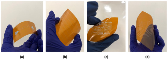
Figure 1.
(a) RFID circuit (b) serpentine circuit (c) microcontroller circuit, and (d) induction coil printed using the magneto hydrodynamic metal jetting process.
A well-documented issue with droplet deposition onto solid substrates is the formation of air pockets inside the deposited droplets after the impingement. The formation of air pockets inside droplets following impact onto a solid substrate has been studied theoretically and experimentally since the early 1990s [19,20,21,22]. The existing scientific consensus about the mechanism is that immediately prior to the droplet impact, a creeping flow of the thin gas layer between the bottom of the droplet and the solid surface is formed [20,23,24,25,26,27]. The gas buildup can create a deformation in the liquid droplet and, subsequently, the thin layer of gas gets entrapped by a circular contact line. As the droplet recoils, the contact line gets contracted and the trapped gas is reshaped into an entrapped bubble. Figure 2 provides an illustration of the bubble evolution in the droplet during impact.
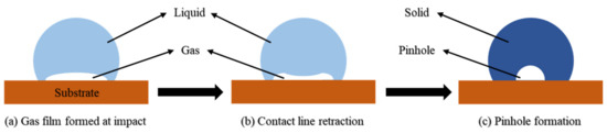
Figure 2.
Schematic of bubble evolution during droplet impact.
When solidification of the droplets is a part of the impingement and rebound process, the trapped bubbles in the solidified droplets are generally referred as pinholes. Relatively few publications have dealt with cases of gas entrapment involving solidification. They include studies on low Weber numbers [28], thermal spray forming [29], and nano pore formation [30]. Work done by Qu et al. interpreted the formation mechanism behind nano scale bubbles observed when nickel drops are deposited onto stainless steel substrates for entrapment of gas during the impingement process and subsequent freezing to a porous solid [30]. Recent work by Yi et al. has demonstrated that the surface roughness of the substrate and the size of the droplet can have an impact on the size and the number of pinholes formed in aluminum molten metal droplets deposited on a brass substrate which is at room temperature [31]. Xiong et al. have performed a numerical investigation of gas entrapment in a molten droplet impacting and solidifying on a cold and smooth substrate by a 3D lattice Boltzmann method [32]. They demonstrated that the trapped gas could form multiple gas pockets, or a single gas pocket, depending on the surface wettability of the substrate. Shukla et al. investigated the effect of substrate wetting on pinhole formation after molten metal droplet impingement and solidification through numerical modelling [33,34].
We note here that the research on the observation of air pockets inside droplets deposited onto polymeric surfaces has been limited to just liquids, excluding phase change from liquid to solid [35]. To the best of our knowledge, research related to pinhole formation in molten metal droplets deposited onto polymer substrates is non-existent. In this work, we report the observations of large pinhole formation in the molten aluminum droplets deposited on a polyimide (PI) substrate for the purpose of fabricating flexible electronic devices. The aims of this study, therefore, are: (1) to provide a hypothesis that explains the pinhole formation mechanism when high temperature molten metal drops are deposited onto polyimide substrates; and (2) to find ways to reduce or eliminate these large pinholes in printed conductive traces. Specifically, we propose a mechanism of pinhole formation and show that the size of the pinholes formed in our case is considerably larger than the size of the pinholes reported in studies where metal droplets are deposited onto metal substrates.
Through a combination of experimental observations and numerical modelling, we demonstrate that the significantly larger pinholes observed in this case are most likely due to the release of adsorbed/absorbed atmospheric humidity from the polymer substrate into the molten metal droplet as it impinges and solidifies on the substrate’s surface. Thermofluidic numerical modelling revealed that the temperature of a significant portion of the substrate underneath the droplet exceeds the boiling point of water as the droplet impacts and solidifies. We propose that the increase in temperature of the substrate beyond 100 °C results in the release of adsorbed moisture from the substrate into the droplet. Subsequently, the escaping gas is trapped in the solidifying droplet and could be the cause of both the large size and the non-equilibrium shape of the pinholes. We also find that the substrate temperature plays a meaningful role on the pinhole size. The size of the pinholes can be reduced considerably by depositing droplets onto substrates at elevated temperature.
2. Materials and Methods
2.1. Materials
High-performance polymers have been prominently used in the microelectronic industry since the 1980s as interdielectric and passivation layers [36]. This is due to their ease of processability and excellent physical, chemical, and thermal properties. Various high-performance polymers such as Polyetheretherketone (PEEK), Polysulfone (PSU), Polyethersulfone (PES), Polyphenylene sulfone (PPSU), and Polyimide (PI) have been employed as dielectric substrates for printed electronic components [37]. Among the high performance polymers, polyimides have found considerable interest for fabrication of devices due to their high thermal stability, excellent chemical resistance, good adhesion behavior with metals and good mechanical properties [36,37,38]. In this study, we have employed a 125 μm (5 mil, 0.005 in) thick polyimide (Kapton® HN, DuPont) film as the flexible polymer substrate. All the experiments were done with as-received polyimide film and no other surface treatments were performed.
2.2. Printing Method
The molten metal jetting system used in this study to deposit aluminum 4043 alloy droplets onto the polymer substrate was the MK1 experimental magnetohydrodynamic liquid metal jetting system manufactured by Xerox Corp, Rochester, NY, USA. For this study, aluminum alloy 4043 was chosen based on the process capabilities of the current printhead configuration in the apparatus. Figure 3 illustrates the magnetohydrodynamic liquid metal jetting process. Metal wire is continuously fed into a heated crucible where it is melted. The bottom of the crucible includes a nozzle with the desired orifice diameter.
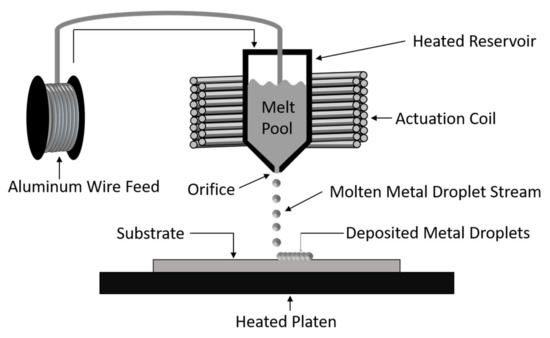
Figure 3.
Cross sectional view of the magnetohydrodynamic liquid metal jetting system and process overview.
The crucible is enveloped by an electromagnetic coil through which direct current flows [39]. By pulsing the electromagnetic coil, a transient magnetic field permeates the molten metal and induces a closed loop transient electric field within it with the pulsing of the electromagnetic coil. This causes circulating eddy currents in the molten metal pool. A magnetohydrodynamic Lorentz force is generated in the chamber as the applied field interacts with the circulating eddy currents and acts to eject a droplet from the orifice. Depending on the ejection parameters, droplets of molten metal are ejected with a velocity of 1–10 m/s and at an ejection frequency of up to 1000 Hz [40]. The crucible is enveloped in argon gas to reduce oxidation of the ejected droplets. The ejected droplets can be deposited at desired locations onto a substrate which rests on a movable platen. The deposited droplets coalesce and solidify to form solid features. In this experimental study, the melt pool temperature was set at 850 °C for printing all the samples. The orifice size employed in the experiments was 500 μm, hence the diameter of ejected droplets is approximately 500 μm.
2.3. Characterization
The printed samples were mounted in an epoxy resin and polished using a Struers Tegramin-20 grinding tool to reveal their internal microstructure. The samples were polished from the side to reveal the cross section of the droplets and to observe any pinholes from the side. The samples were also polished from the bottom to remove the substrate, reveal the bottom of the droplet, and observe the pinholes from the bottom. A Hirox KH-7700 optical microscope was used to take the micrographs of the polished samples.
3. Results and Discussion
3.1. Numerical Modeling
The hypothesis that the adsorbed/absorbed moisture from the substrate is being released into the droplet relies on the assumption that the entire substrate underneath the solidifying droplet experiences a temperature beyond the boiling point of water. Quantifying this temperature rise in the substrate as a single 500 μm diameter droplet impinges onto it can be extremely difficult through an experimental approach. A numerical model that would consider the droplet and substrate properties can provide a reasonably accurate description of the thermodynamics as a metal droplet impacts the substrate.
Flow-3D numerical modeling software was employed to simulate the process of droplet impact, flattening, and solidification. The simulation was performed by solving fluid flow, energy, and solidification equations on a 3D grid. Figure 4 shows a schematic of the computational domain used to study droplet impingement. The droplet is initialized with a setpoint temperature, velocity, and size obtained from experiments. It is assumed to be spherical and completely in the liquid state before it impacts vertically on the stationary substrate composed of a layer of polyimide on top of a brass platen. The droplet then flattens, rebounds, and solidifies according to the computational model as temperature, flow and solid fraction variables are tracked locally.
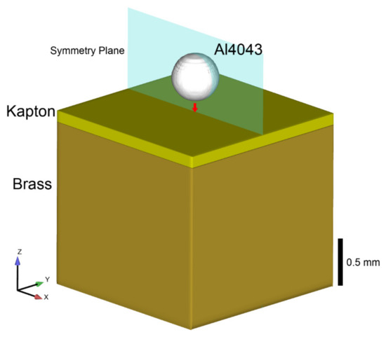
Figure 4.
Schematic of the droplet impingement model.
The following assumptions dictate the limitations of the model:
- The flow inside the molten droplet was treated as incompressible and laminar.
- The flow and heat transfer of the surrounding gas was ignored to improve computational time.
- The material properties of the metal were temperature-dependent, while the material properties of the polyimide and brass were held constant.
- The heat transfer is dominated by conduction and to a lesser extent, convection modes, ignoring radiation from the droplet surface to the surroundings.
- Convection to the outside gas is approximated with a constant heat transfer coefficient since the solidification is dominated by conduction to the substrate.
- Droplet was assumed to be free of oxidation.
- Plane symmetry is assumed in the y-direction across the middle of the droplet. This is used to reduce computational time.
- Material properties were assumed to be isotropic and homogeneous.
The model solves the Navier–Stokes equations using the volume of fluid (VOF) method to define the two phases and the free surface. The approach considers the thermo-fluidic heat transfer and solidification at temperature T for appropriate initial and boundary conditions:
where I is the specific energy of the fluid defined as:
cp and k are the specific heat at constant pressure and thermal conductivity of a material, respectively, L is the latent heat of fusion for the aluminum alloy, and fs is the local solid fraction. fs is the local ratio of the solidified material to the total material in the computational domain and is used to determine the state of solidification within a fluid. It is evaluated by comparing the temperature inside the fluid to the material dependent solidus (Ts) and liquidus (Tl) temperatures, until the latent heat (L) is extracted from the fluid. The solid fraction approaches unity as the local latent heat is released.
The entire domain shown in Figure 4 was modeled. The gaseous domain was 2 mm long (x), 1 mm wide (y) and the substrate was 125 μm thick. A symmetry boundary condition extended in the x-direction. The domain was meshed with a uniform size of 20 μm per element. All zones were initialized with a temperature of 30 °C. The diameter of the drop was 490 μm. The initial temperature and velocity of the droplet were patched at 775 °C and 2.5 m/s, respectively. The physical properties of the Al 4043 droplet used in the model are provided in Table 1. The polyimide substrate temperature is set as 30 °C in the first simulation and 150 °C in the second simulation. The simulation starts when the droplet is 475 μm from the substrate. The model inputs are provided in Table 2.

Table 1.
Physical properties of Aluminum droplet used in the current model.
Table 2.
Model inputs.
Figure 5 shows the phase profile of impinging droplet and the solidification front at different times. The droplet starts to spread on the substrate in the radial direction immediately after impact. The flattening of the droplet finishes at ~400 μs. The solidification starts occurring at about ~13 ms and finishes at 250 ms. The simulated drop has a similar morphology to solidified drops observed via physical experimentation described in Section 3.2. The solidification of the droplet can be seen to be happening from the edges inward and from the bottom to the top of the droplet, in line with physical intuition.
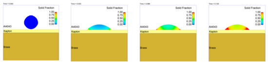
Figure 5.
Fluid fraction of impinging droplet and the solidification front at different times. Solid fraction of 1 implies a fully solid region.
The substrate temperature versus distance beneath the top surface of the substrate is plotted at different time intervals following impact of the droplet with the substrate in Figure 6 (unheated substrate) and Figure 7 (substrate heated to 150 °C). It can be noted from Figure 6 and Figure 7 that almost the entire substrate thickness underneath the droplet experiences an increase in temperature to well over 100 °C. It is also worth noting that substrate heating has essentially no effect on the maximum temperature at any location in the substrate. It only affects the minimum temperature after cooling and solidification has taken place.
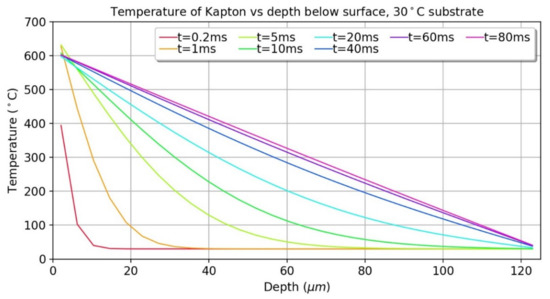
Figure 6.
Substrate temperature versus depth beneath the substrate’s top surface when the substrate is unheated (30 °C).
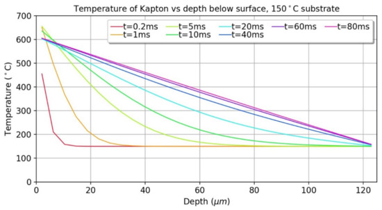
Figure 7.
Substrate temperature versus depth beneath the substrate’s top surface when the substrate is heated to 150 °C.
Figure 5, Figure 6 and Figure 7 show that a significant portion of the polyimide substrate experiences a temperature of over 100 °C (i.e., the boiling point of water) as the droplet solidifies. Complete solidification of the deposited aluminum is not reached until 250 milliseconds. A significant portion of the substrate underneath the droplet is noted to be over 100 °C during that time. The increase in the substrate temperature to beyond the boiling point of water shows the feasibility of adsorbed moisture in the substrate vaporizing and escaping into the droplet that is still in the liquid phase.
3.2. Experimental Results
Experimental observations reveal the presence of large pinholes when molten Al4043 droplets jetted at 850 °C are deposited onto polyimide Kapton HN substrate which is rests on an unheated (i.e., room temperature) platen. Figure 8 presents the micrographs of the bottom and side cross section of the solidified Al4043 droplets deposited on Kapton substrate. The presence of multiple pinholes can be clearly observed from the bottom and side view micrographs. A considerably large pinhole can also be observed in the side view. Surface profiles taken using a Nanovea white light interferometry profilometer confirmed that the observed features inside the solidified metal droplets are indeed voids.
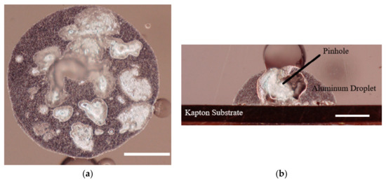
Figure 8.
(a) Bottom view of a printed droplet and (b) side view of the droplet cross-section. Scale bar = 250 µm.
The approximate diameter of a pinhole was measured using the Hirox KH-7700 optical microscope as illustrated in Figure 9. The radius of the pinhole was approximately 122 μm for a 500 μm diameter droplet. The pinhole size is highly reproducible from numerous samples printed at similar experimental conditions.
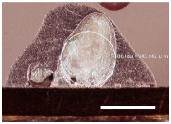
Figure 9.
Approximate 245 µm diameter of a pinhole being measured on a Hirox microscope. Scale bar = 250 µm.
Yi et al. have studied the pinhole formation behavior when molten aluminum droplets are deposited onto a brass substrate [31]. Based on their experimental observations, they have developed a mathematical formulation for predicting the pinhole size when molten metal droplets are deposited onto solid substrates. The formula shown in Equation (3) predicts the radius of the pinhole (Rp) by considering the gas dynamic viscosity (μg) of the gas surrounding the droplet, surface tension of the droplet (σ), the droplet radius before impact (R), the liquid mass density () and the Stokes number—defined by St = RU/μg, wherein (U) is the droplet impact velocity.
For the typical experimental conditions used in this work, R = 250 μm, ρl = 2700 kg·m−3, U = 1–10 m/s [40,41] and μg = 5.04 × 10⁻⁵ Pa.s. This assumes that the temperature of the argon gas surrounding the droplet is approximately 700 °C [42]) and σ = 0.77 N/m [43]. Using these values with Equation (3), the predicted radius of the pinholes in the droplet impact velocity range of 1–10 m/s is calculated to be in the range of 10–22 μm. However, the measured value of the pinhole radius in our case is ~122 μm. Hence the formulation does not explain the formation of the large pinholes in our current study.
Through experimental investigation, it was discovered that the size of the pinholes can be reduced considerably when droplets are deposited onto heated substrates rather than room temperature substrates. Figure 10 and Figure 11 show side and bottom views of droplets printed on polyimide substrates which were at temperatures of 25 °C, and 150 °C, respectively. The size of the pinholes is dramatically smaller when the droplets are deposited onto the heated substrate. The average radius of the pinholes measured when droplets are deposited onto the heated polyimide substrate was ~22 μm. This lies within the range of pinhole diameter that is predicted by the formulation developed by Yi et al. [31].
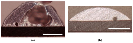
Figure 10.
Side view of the deposited droplet printed at substrate temperature of (a) 25 °C and (b) 150 °C. Scale bar = 250 µm.
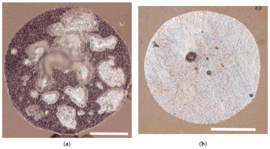
Figure 11.
Bottom view of the deposited droplet printed at substrate temperature of (a) 25 °C and (b) 150 °C. Scale bar = 250 µm.
We hypothesize that the significantly larger pinholes in the droplets formed on a room temperature substrate is due to the release of absorbed moisture from the substrate into the solidifying droplet. Kapton is a hygroscopic material with a moisture absorption percentage of 1.8% at 50% RH and 23°C [44]. As the molten aluminum droplets land on the substrate, the temperature of the polyimide increases beyond the boiling point of water, as predicted via numerical simulation (Figure 6 and Figure 7). The large pinholes are formed as the droplet solidifies around the water vapor escaping from the substrate.
When the substrate is heated to 150 °C, the absorbed moisture is driven off. Prior studies have shown that heating Kapton HN to over 100 °C for a few minutes can remove the majority of absorbed moisture [45]. As droplets are deposited onto the heated substrate, any pinholes formed are then most likely due to the entrapment of surrounding gas beneath the impinging droplet, as proposed by earlier studies [23,24,25]. The size of the pinholes observed when droplets are deposited onto the heated polymer substrates correlates well with the size of pinholes observed when metal droplets are deposited onto metallic substrates, thereby further corroborating the hypothesis.
In a follow-up experiment, the effectiveness of pre-drying the substrate to remove the moisture and printing onto it without substrate heating would have an effect on pinhole formation. The polyimide substrates were dried in a vacuum oven for 12 h at 250 °C to remove any adsorbed moisture. The dried substrate was placed on the unheated print bed, and 850 °C aluminum alloy droplets were deposited. Figure 12 show the pinholes when droplets were directly deposited onto undried and dried Kapton substrates respectively. Somewhat surprisingly, pinholes in droplets deposited onto the pre-dried substrates were comparable in size to the pinholes in the undried substrate.
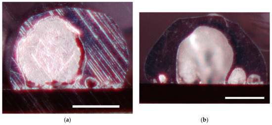
Figure 12.
Pinholes in (a) undried and (b) dried substrate. Scale bar = 250 µm.
Prior studies have shown that dried polyimide can adsorb atmospheric moisture at a fast rate [46,47]. In this case, the dried polyimide was transported from the vacuum oven to the printer in a desiccator with desiccant in it. However, there was a delay of ~15 min between the time the dried substrates were mounted in the printer and the time the droplets were jetted. During this time, the substrates were exposed to open atmosphere. To assess how much moisture might be gained during that time span, the masses of ten Kapton samples were measured immediately after drying. Those same samples were then weighed after 15 min of exposure to open atmosphere. The mass of the samples increased by an average of 0.6% after 15 min of exposure to open atmosphere. The presence of pinholes in dried substrates could therefore be explained by the possibility of reabsorption of moisture between drying and printing. This underscores the importance of substrate heating with hygroscopic substrates.
Following experiments involving the interaction of individual drops with heated and unheated substrates, continuous linear electronic traces were printed onto unheated and heated polyimide substrates at a deposition frequency of 40 Hz and drop spacing of 300 μm. Figure 13 shows the cross-sectional images of conductive traces printed onto unheated (~25 °C) and heated (150 °C) substrates. Compared to the unheated substrate, there are fewer pinholes in the traces printed on the heated substrate and they are much smaller in size. It can also be noted that the thickness of traces printed on the heated substrate is considerably smaller than the thickness of the traces printed on the unheated substrate. Both traces were printed using identical jetting parameters and therefore have the same volume of metal per millimeter of trace length. However, the large pinholes in traces printed on the unheated substrate result in significant distortion of the trace.
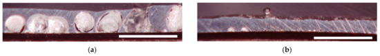
Figure 13.
Longitudinal cross-section of tracks printed on substrate at (a) 25 °C (b) 150 °C. Scale bar = 1000 µm.
As the printed tracks are intended for use in flexible electronics, the minimization of pinhole quantity and size is highly desirable. A lack of pinholes can improve the substrate adhesion of the printed traces due to the higher contact area of the metal with the substrate. The presence of pinholes can also make printed traces highly susceptible to crack formation near the pinholes when the substrate is flexed. Smaller pinholes can greatly improve the performance of the printed features when they are subjected to bending due to the reduced number of regions where crack propagation could begin. Interestingly, no significant variation in electrical resistivity was observed between samples printed with and without substrate heating. This is most likely because the amount of aluminum is same in both the tracks with and without pinholes.
4. Conclusions and Future Work
Large pinholes were observed when droplets of molten aluminum were deposited onto room temperature polyimide substrates for the purpose of fabricating flexible electronic circuits. The formation mechanism behind the pinholes was explained as the release of adsorbed moisture from the polyimide into the solidifying droplet. Heating of the substrate above the boiling point of water was shown to dramatically reduce the number and size of pinholes due to the removal of adsorbed moisture through the heating process. Depositing aluminum droplets onto a pre-dried substrate is not recommended if the substrate is exposed to open atmosphere for a period after drying, as there is a chance for the reabsorption of moisture. Numerical modeling revealed that the temperature of the substrate underneath the metal droplet exceeds 100 °C while the droplet is still in liquid phase. This supports the hypothesis that absorbed moisture evaporates into the deposited droplet. Using high performance polymers with low absorption coefficients could be a potential way of reducing the size of pinholes when molten metal jetting is used for printed electronics applications. Substrate heating to beyond 100 °C is shown to be an effective approach for reducing the quantity and size of pinholes.
The work reported in this paper used relatively large diameter (500 μm) nozzles. Printed traces this large are extremely well suited for high power printed electronics that must carry large currents. This is particularly true given the large cross-sectional area of the printed traces compared with nanoparticle ink traces that tend to be just a few microns thick. However, many printed electronics applications require narrower traces. Experimentation using smaller diameter nozzles (150 μm and 250 μm) have indicated that much narrower traces can successfully be printed with this technique. Future work will include consideration of how substrate heating may or may not affect results as drop size decreases. On the one hand, the volume of a drop, and hence the thermal energy carried within the drop, is a function of the cube of the radius. As drop size decreases, the thermal energy therefore decreases rapidly. However, the drops still have a temperature of ~900 °C on impact with the substrate. It is therefore likely that some water vapor will be released into the molten metal if the substrate is not heated. Figure 8b and Figure 10a both show examples where a gas pocket actually pierces through the top of the printed trace. As printed trace size decreases, even smaller diameter gas pockets have potential to result in complete voids in a printed trace. This theory will be tested in future experiments with smaller diameter nozzles.
Author Contributions
Conceptualization, M.M. and D.C.; methodology, M.M., D.C. and V.S.; software, V.S.; validation, M.M.; formal analysis, M.M., V.S. and D.C.; resources, D.C.; writing—original draft preparation, M.M. and V.S.; writing—review and editing, D.C.; visualization, M.M. and V.S.; supervision, D.C.; project administration, D.C.; funding acquisition, D.C. All authors have read and agreed to the published version of the manuscript.
Funding
This research was funded by the New York Empire State Development Corporation, grant number C150122.
Conflicts of Interest
V.S. was employed part-time by Xerox while working towards his PhD degree. He contributed the Flow3D numerical process modeling, and he authored the portion of the paper detailing numerical simulation and analysis results.
References
- Cantatore, E. Applications of organic and printed electronics. In A Technology-Enabled Revolution; Springer: New York, NY, USA, 2013. [Google Scholar]
- Chang, J.S.; Facchetti, A.F.; Reuss, R. A Circuits and Systems Perspective of Organic/Printed Electronics: Review, Challenges, and Contemporary and Emerging Design Approaches. IEEE J. Emerg. Sel. Top. Circuits Syst. 2017, 7, 7–26. [Google Scholar] [CrossRef]
- Tong, G.; Jia, Z.; Chang, J. Flexible Hybrid Electronics: Review and Challenges. In Proceedings of the 2018 IEEE International Symposium on Circuits and Systems (ISCAS), Florence, Italy, 27–30 May 2018; pp. 1–5. [Google Scholar] [CrossRef]
- Huang, Q.; Zhu, Y. Printing conductive nanomaterials for flexible and stretchable electronics: A review of materials, processes, and applications. Adv. Mater. Technol. 2019, 4, 1800546. [Google Scholar] [CrossRef]
- Rocha, L.A.; Viana, J.C. Printing Technologies on Flexible Substrates for Printed Electronics. In Flexible Electronics; InTechOpen: Rijeka, Croatia, 2018. [Google Scholar]
- Perelaer, B.J.; De Laat, A.W.M.; Hendriks, C.E.; Schubert, U.S. Inkjet-printed silver tracks: Low temperature curing and thermal stability investigation. J. Mater. Chem. 2008, 18, 3209–3215. [Google Scholar] [CrossRef]
- Smith, P.J.; Shin, D.-Y.; Stringer, J.E.; Derby, B.; Reis, N. Direct ink-jet printing and low temperature conversion of conductive silver patterns. J. Mater. Sci. 2006, 41, 4153–4158. [Google Scholar] [CrossRef]
- Van Osch, T.T.; Perelaer, J.J.; De Laat, A.W.M.; Schubert, U.U. Inkjet Printing of Narrow Conductive Tracks on Untreated Polymeric Substrates. Adv. Mater. 2007, 20, 343–345. [Google Scholar] [CrossRef]
- Kamyshny, A.; Magdassi, S. Conductive Nanomaterials for Printed Electronics. Small 2014, 10, 3515–3535. [Google Scholar] [CrossRef] [PubMed]
- Perelaer, J.; Smith, P.J.; Mager, D.; Soltman, D.; Volkman, S.K.; Subramanian, V.; Korvink, J.; Schubert, U.S. Printed electronics: The challenges involved in printing devices, interconnects, and contacts based on inorganic materials. J. Mater. Chem. 2010, 20, 8446–8453. [Google Scholar] [CrossRef]
- Agina, E.V.; Sizov, A.S.; Yablokov, M.Y.; Borshchev, O.V.; Bessonov, A.A.; Kirikova, M.N.; Bailey, M.J.A.; Ponomarenko, S.A. Polymer Surface Engineering for Efficient Printing of Highly Conductive Metal Nanoparticle Inks. ACS Appl. Mater. Interfaces 2015, 7, 11755–11764. [Google Scholar] [CrossRef] [PubMed]
- Roshanghias, A.; Krivec, M.; Baumgart, M. Sintering strategies for inkjet printed metallic traces in 3D printed electronics. Flex. Print. Electron. 2017, 2, 045002. [Google Scholar] [CrossRef]
- Arsenov, P.V.; Efimov, A.A.; Ivanov, V.V. Comparison of Thermal and Electrical Sintering of Aerosol Silver Nanoparticles in Process of Aerosol Jet Printing. Key Eng. Mater. 2020, 834, 10–15. [Google Scholar] [CrossRef]
- Jang, Y.-R.; Joo, S.-J.; Chu, J.-H.; Uhm, H.-J.; Park, J.-W.; Ryu, C.-H.; Yu, M.-H.; Kim, H.-S. A Review on Intense Pulsed Light Sintering Technologies for Conductive Electrodes in Printed Electronics. Int. J. Precis. Eng. Manuf. Technol. 2021, 8, 327–363. [Google Scholar] [CrossRef]
- Chung, W.-H.; Hwang, H.-J.; Kim, H.-S. Flash light sintered copper precursor/nanoparticle pattern with high electrical conductivity and low porosity for printed electronics. Thin Solid Films 2015, 580, 61–70. [Google Scholar] [CrossRef]
- Cost of 4043 Aluminum Wire. Available online: https://www.airgas.com/product/Welding-Products/Filler-Metal/MIG-Wire-%28GMAW-%26-SAW%29/MIG-Wire---Aluminum/p/RAD64001502 (accessed on 23 April 2021).
- Cost of Aluminum Nanoparticles. Available online: https://www.ssnano.com/inc/sdetail/aluminum_nanoparticles__nanopowder__al__99_7__40_60_nm_/276 (accessed on 23 April 2021).
- Kamyshny, A.; Steinke, J.; Magdassi, S. Metal-based ink jet inks for printed electronics. Open Appl. Phys. J. 2011, 4, 1835–1874. [Google Scholar] [CrossRef]
- Chandra, S.; Avedisian, C.T. On the collision of a droplet with a solid surface. Proc. R. Soc. Lond. Ser. A Math. Phys. Sci. 1991, 432, 13–41. [Google Scholar] [CrossRef]
- Lee, J.S.; Weon, B.M.; Je, J.H.; Fezzaa, K. How Does an Air Film Evolve into a Bubble During Drop Impact? Phys. Rev. Lett. 2012, 109, 204501. [Google Scholar] [CrossRef] [Green Version]
- Xu, L.; Zhang, W.W.; Nagel, S.R. Drop Splashing on a Dry Smooth Surface. Phys. Rev. Lett. 2005, 94, 184505. [Google Scholar] [CrossRef] [Green Version]
- Bouwhuis, W.; van der Veen, R.; Tran, T.; Keij, D.L.; Winkels, K.G.; Peters, I.; Van Der Meer, D.; Sun, C.; Snoeijer, J.H.; Lohse, D. Maximal Air Bubble Entrainment at Liquid-Drop Impact. Phys. Rev. Lett. 2012, 109, 264501. [Google Scholar] [CrossRef]
- de Ruiter, J.; Oh, J.M.; van den Ende, D.; Mugele, F. Dynamics of collapse of air films in drop impact. Phys. Rev. Lett. 2012, 108, 074505. [Google Scholar] [CrossRef] [Green Version]
- Driscoll, M.; Nagel, S.R. Ultrafast Interference Imaging of Air in Splashing Dynamics. Phys. Rev. Lett. 2011, 107, 154502. [Google Scholar] [CrossRef] [Green Version]
- Josserand, C.; Thoroddsen, S.T. Drop Impact on a Solid Surface. Annu. Rev. Fluid Mech. 2016, 48, 365–391. [Google Scholar] [CrossRef] [Green Version]
- de Ruiter, J.; van den Ende, D.; Mugele, F. Air cushioning in droplet impact. II. Experimental characterization of the air film evolution. Phys. Fluids 2015, 27, 012105. [Google Scholar] [CrossRef] [Green Version]
- Kolinski, J.; Rubinstein, S.M.; Mandre, S.; Brenner, M.P.; Weitz, D.A.; Mahadevan, L. Skating on a Film of Air: Drops Impacting on a Surface. Phys. Rev. Lett. 2012, 108, 074503. [Google Scholar] [CrossRef] [Green Version]
- Schiaffino, S.; Sonin, A.A. Molten droplet deposition and solidification at low Weber numbers. Phys. Fluids 1997, 9, 3172–3187. [Google Scholar] [CrossRef]
- Mehdi-Nejad, V.; Mostaghimi, J.; Chandra, S. Air bubble entrapment under an impacting droplet. Phys. Fluids 2003, 15, 173–183. [Google Scholar] [CrossRef]
- Qu, M.; Wu, Y.; Srinivasan, V.; Gouldstone, A. Observations of nanoporous foam arising from impact and rapid solidification of molten Ni droplets. Appl. Phys. Lett. 2007, 90, 254101. [Google Scholar] [CrossRef]
- Yi, H.; Qi, L.-H.; Luo, J.; Jiang, Y.; Deng, W. Pinhole formation from liquid metal microdroplets impact on solid surfaces. Appl. Phys. Lett. 2016, 108, 041601. [Google Scholar] [CrossRef]
- Xiong, W.; Cheng, P. Numerical investigation of air entrapment in a molten droplet impacting and solidifying on a cold smooth substrate by 3D lattice Boltzmann method. Int. J. Heat Mass Transf. 2018, 124, 1262–1274. [Google Scholar] [CrossRef]
- Shukla, R.K.; Kumar, A.; Kumar, R.; Singh, D.; Kumar, A. Numerical study of pore formation in thermal spray coating process by investigating dynamics of air entrapment. Surf. Coatings Technol. 2019, 378, 124972. [Google Scholar] [CrossRef]
- Kumar, R.; Shukla, R.K.; Kumar, A.; Kumar, A. A computational study on air entrapment and its effect on convective heat transfer during droplet impact on a substrate. Int. J. Therm. Sci. 2020, 153, 106363. [Google Scholar] [CrossRef]
- Pittoni, P.G.; Lin, Y.-C.; Wang, R.-J.; Yu, T.-S.; Lin, S.-Y. Bubbles entrapment for drops impinging on polymer surfaces: The roughness effect. Exp. Therm. Fluid Sci. 2015, 62, 183–191. [Google Scholar] [CrossRef]
- Ree, M.; Han, H.; Gryte, C.C. Water sorption in thin films of high-temperature polyimides: The effect of imidization history. High Perform. Polym. 1994, 6, 321–333. [Google Scholar] [CrossRef]
- McKeen, L.W. Film Properties of Plastics and Elastomers; William Andrew Publishing: Norwich, NY, USA, 2012. [Google Scholar]
- Mittal, K.L. Polyimides: Synthesis, Characterization, and Applications; Springer Science & Business Media: Berlin/Heidelberg, Germany, 2013; Volume 1. [Google Scholar]
- Vader, S.; Vader, Z. Conductive Liquid three Dimensional Printer. US20170182553A1, 7 August 2018. [Google Scholar]
- Karampelas, I.H.; Vader, S.; Vader, Z.; Sukhotskiy, V.; Verma, A.; Garg, G.; Tong, M.; Furlani, E. Drop-on-demand 3D metal printing. Inform. Electron. Microsyst. 2017, 4, 153–155. [Google Scholar]
- Sukhotskiy, V.; Karampelas, I.H.; Garg, G.; Verma, A.; Tong, M.; Vader, S.; Vader, Z.; Furlani, E.P. Magnetohydrodynamic drop-on-demand liquid metal 3D printing. In Proceedings of the Solid Freeform Fabrication, Austin TX, USA, 7–9 August 2017. [Google Scholar]
- Kestin, J.; Ro, S.T.; Wakeham, W.A. Viscosity of the noble gases in the temperature range 25–700 °C. J. Chem. Phys. 1972, 56, 4119–4124. [Google Scholar] [CrossRef]
- Bainbridge, I.F.; Taylor, J.A. The Surface Tension of Pure Aluminum and Aluminum Alloys. Met. Mater. Trans. A 2013, 44, 3901–3909. [Google Scholar] [CrossRef]
- Dupont™ Kapton® Summary of Properties. Available online: https://www.dupont.com/content/dam/dupont/amer/us/en/products/ei-transformation/documents/DEC-Kapton-summary-of-properties.pdf (accessed on 5 August 2020).
- Haghighi, H.; Cotton, I. Analysis of the Degradation Kinetics of Kapton Film in an Aerospace Environment. In Proceedings of the 2019 IEEE Electrical Insulation Conference (EIC), Calgary, AB, Canada, 16–19 June 2019; pp. 1–4. [Google Scholar]
- Yang, D.K.; Koros, W.J.; Hopfenberg, H.B.; Stannett, V.T. Sorption and transport studies of water in Kapton polymide. I. J. Appl. Polym. Sci. 1985, 30, 1035–1047. [Google Scholar] [CrossRef]
- Akram, M.; Jansen, K.M.B.; Bhowmik, S.; Ernst, L.J. Moisture absorption analysis of high performance polyimide adhesive. In Proceedings of the SAMPE Fall Technical Conference 2011, Fort Worth, TX, USA, 17–20 October 2011. [Google Scholar]
Publisher’s Note: MDPI stays neutral with regard to jurisdictional claims in published maps and institutional affiliations. |
© 2021 by the authors. Licensee MDPI, Basel, Switzerland. This article is an open access article distributed under the terms and conditions of the Creative Commons Attribution (CC BY) license (https://creativecommons.org/licenses/by/4.0/).