Abstract
This study presents a hard-switching full-bridge DC-DC converter with synchronous rectification based on Gallium Nitride (GaN) transistors to evaluate the advantages of GaN devices in power supplies. In comparison to traditional silicon-based devices, GaN transistors are utilized in both the primary and secondary stages of the converter, exploiting GaN’s lower on-resistance to enhance performance. The converter operates at a switching frequency of 300 kHz, with an input voltage range of 36 V to 75 V, delivering an output of 28 V/42 A. Experimental results show that the GaN-based converter achieves an output power of 1176 W within standard half-brick package dimensions. The measured peak efficiency is 97.1%, and the power density reaches 430 W/in3. These findings demonstrate that GaN-based converters offer superior efficiency and power density compared to conventional silicon-based designs, making them highly suitable for aerospace, automotive, and communication power supplies.
1. Introduction
Isolated DC-DC converters are used in various applications such as power systems, renewable energy solutions, automotive, aerospace, and communication power supplies [1], due to their attractive characteristics like high efficiency, power density, and reliability, and are particularly important for powering 28 V DC, which is a standard power supply for many electrical and electronic components [2].
Over decades of development, silicon-based power devices have seen remarkable performance improvements, approaching the intrinsic material limits of silicon. However, their performance has plateaued [3], leaving traditional silicon-based power converters unable to meet the emerging demands of consumer electronics, and other advanced applications. Third-generation semiconductor materials, such as gallium nitride (GaN), have garnered significant attention for their wide bandgap and high critical breakdown field strength. GaN transistors, characterized by low parasitic parameters, low on-resistance, and reduced switching losses [4,5,6,7], offer significant advantages in enhancing switching frequency, efficiency, and power density, making them well-suited for new application scenarios in power conversion [8,9,10,11,12].
High-frequency power conversion circuits are available in various configurations, including flyback, forward, push-pull, half-bridge, and full-bridge topologies [13]. Among these, full-bridge converters stand out for their ability to enable bidirectional transformer magnetization, resulting in more efficient core utilization [14]. Compared to flyback, forward, and push-pull circuits, full-bridge converters require power switches with lower voltage ratings [15,16]. In contrast to half-bridge converters, full-bridge designs eliminate the need for a capacitor bridge arm, while halving the current through each switch for a given power level [17,18,19]. This simplifies circuit design and improves reliability. For these reasons, this work adopts the full-bridge converter as the preferred power topology.
This paper presents a hard-switching full-bridge converter with synchronous rectification, where GaN transistors are utilized to replace conventional silicon-based power devices for both the primary-side power switches and the secondary-side synchronous rectifiers. The system achieves an efficiency of up to 97.1% at an output power of 1176 W. The proposed converter offers several advantages, including reduced size, improved efficiency, lower ripple, and enhanced dynamic response. It effectively meets the power supply requirements [20,21,22,23,24,25], which demand high output power and superior conversion efficiency.
2. Circuit Structure and Operating Principle of the Converter
2.1. Proposed Circuit Structure
The schematic of the proposed hard-switching full-bridge DC/DC converter with synchronous rectification is illustrated in Figure 1. The primary side comprises two bridge arms, with each arm constructed using two GaN transistors. The primary winding (NP) of the high-frequency transformer is connected between the midpoints of the two bridge arms.
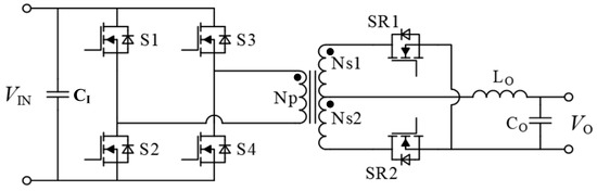
Figure 1.
Schematic diagram of the proposed hard-switching full-bridge converter.
On the secondary side, GaN transistors SR1 and SR2 are employed as synchronous rectifiers, replacing conventional diodes. Due to the significantly lower on-resistance of GaN transistors compared to the forward voltage drop of diodes, the use of synchronous rectification technology effectively reduces conduction losses and enhances the efficiency of the converter. Additionally, the reduced thermal stress on the components contributes to improved reliability and facilitates the miniaturization of the power supply [26].
The output filter, composed of an inductance LO and a capacitance CO, forms a low-pass filtering network that smooths the output voltage and ensures stable DC delivery. All switches S1 to S4 on the primary side, as well as the synchronous rectifiers SR1 and SR2 on the secondary side, are implemented using GaN transistors. Compared to silicon-based MOSFETs, GaN transistors offer significantly lower on-resistance and reduced parasitic parameters at equivalent voltage ratings. This enables lower driving, conduction, and switching losses. Furthermore, the absence of reverse recovery losses in GaN transistors contributes to enhanced overall efficiency. The parameters of the proposed converter are listed in Table 1.

Table 1.
Parameters of the proposed converter.
2.2. Operating Principle of the Main Circuit
The proposed converter operates in the pulse width modulation (PWM) control mode. Figure 2 depicts the gate drive waveforms of the primary and secondary GaN transistors, along with the primary voltage waveform (VNp) of the transformer during steady-state operation.
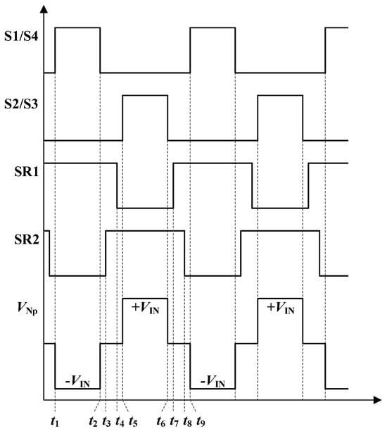
Figure 2.
Steady-state operating waveforms.
The proposed hard-switching full-bridge converter with synchronous rectification operates in a cyclic manner, with each switching period comprising eight distinct modes. The detailed analysis of these modes is as follows:
- State 1 (t1~t2): Energy Transmission PhaseDuring this phase, the primary-side switches S1 and S4 are turned on, while S2 and S3 remain off. The synchronous rectifier SR1 on the secondary side is conducting, while SR2 is reverse-biased and non-conducting. The input voltage (VIN) is directly applied across the primary winding of the transformer, resulting in negative polarity at the same-name terminal. Energy is transferred from the input to the output, the transformer is magnetized, and the inductor current (ILₒ) increases linearly.
- State 2 (t2~t3): Freewheeling PhaseAt this stage, all primary-side switches (S1 to S4) are turned off, and the voltages across the transformer windings are zero, maintaining constant magnetizing current. The synchronous rectifier SR1 remains on, while SR2 is off. Current flows through the channel of SR1 and the body diode of SR2, ensuring continuity of load current. This phase corresponds to the dead time between S1/S4 and SR2.
- State 3 (t3~t4): Freewheeling PhaseIn this phase, all primary-side switches (S1 to S4) remain off, while both SR1 and SR2 on the secondary side are conducting. The transformer primary and secondary voltages are zero, and the magnetizing current remains unchanged. Current flows simultaneously through the channels of SR1 and SR2, maintaining load continuity.
- State 4 (t4~t5): Freewheeling PhaseAt this stage, all primary-side switches (S1 to S4) remain off, and the transformer primary and secondary voltages remain zero. The synchronous rectifier SR1 turns off, while SR2 remains on. Current flows through the body diode of SR1 and the channel of SR2. This phase corresponds to the dead time between S2/S3 and SR1.
- State 5 (t5~t6): Energy Transmission PhaseDuring this phase, the primary-side switches S2 and S3 are turned on, while S1 and S4 remain off. On the secondary side, SR2 is conducting, while SR1 is reverse-biased and non-conducting. The input voltage (VIN) is directly applied to the primary winding of the transformer, resulting in positive polarity at the same-name terminal. Energy is transferred from the input to the output, the transformer is magnetized, and the inductor current (ILₒ) increases linearly.
- State 6 (t6~t7): Freewheeling PhaseAt this stage, all primary-side switches (S1 to S4) are turned off, and the voltages across the transformer windings are zero, maintaining constant magnetizing current. The synchronous rectifier SR1 is off, while SR2 remains on. Current flows through the body diode of SR1 and the channel of SR2. This phase corresponds to the dead time between S2/S3 and SR1.
- State 7 (t7~t8): Freewheeling PhaseIn this phase, all primary-side switches (S1 to S4) remain off, while both SR1 and SR2 on the secondary side are conducting. The transformer primary and secondary voltages are zero, and the magnetizing current remains unchanged. Current flows simultaneously through the channels of SR1 and SR2, maintaining load continuity.
- State 8 (t8~t9): Freewheeling PhaseDuring this phase, all primary-side switches (S1 to S4) are turned off, and the transformer primary and secondary voltages remain zero. The synchronous rectifier SR1 is conducting, while SR2 is off. Current flows through the channel of SR1 and the body diode of SR2. This phase corresponds to the dead time between S1/S4 and SR2.
- State 9 (t9)At t9, the converter transitions back to state 1, repeating the same sequence for the next switching cycle.
Figure 3 shows the current or voltage waveforms to illustrate the working principle of the converter. The simulation verifies that the waveforms of S1–S4 and SR1–SR2 align with the expected results.
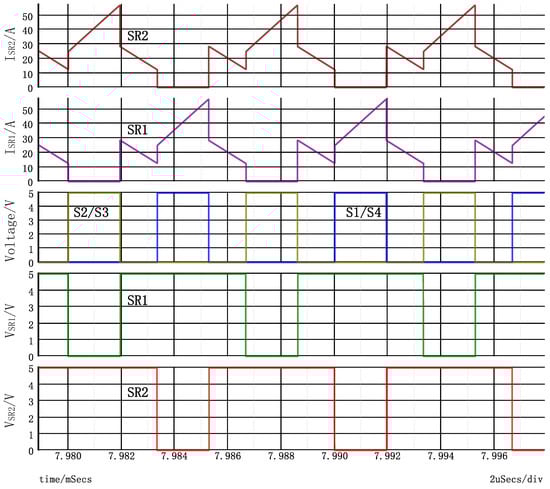
Figure 3.
Current or voltage waveforms of S1–S4 and SR1–SR2.
3. Experimental Results
Figure 4 shows the prototype of the fabricated hard-switching full-bridge converter. The measurements are performed using the ITECH IT8814 electronic load (ITECH ELECTRONIC Co., Ltd.; Nanjing; China.), which offers high resolution and precision. The power converter was tested under a rated input voltage of 36 V, 48 V, and 75 V. The efficiency over the entire load range is presented in Figure 5. At the nominal input voltage of 48 V, the peak efficiency is 97.1%, achieved at 70% load, while the full-load efficiency is 96.6%. At an input voltage of 36 V, the efficiency improves by approximately 0.2%. However, at an input voltage of 75 V, there is a slight decrease in efficiency of about 1%. Despite load variations, the efficiency remains consistently high. Compared to silicon-based MOSFETs, GaN transistors exhibit significantly lower switching losses. Even with an increased switching frequency of 300 kHz, the hard-switching full-bridge converter maintains high efficiency, highlighting the advantages of GaN transistors in high-frequency power conversion applications.
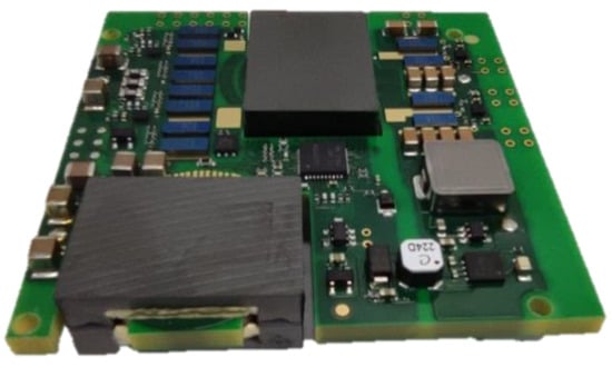
Figure 4.
The fabricated hard-switching full-bridge converter prototype.
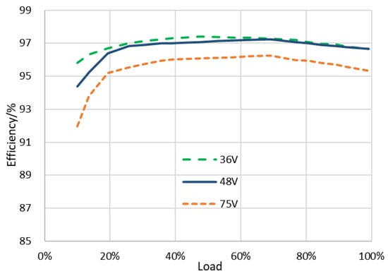
Figure 5.
Measured efficiency curve of the converter.
Figure 6 shows the ripple waveform of the output voltage under rated input voltage of 48 V and full-load conditions. The GaN-based hard-switching full-bridge converter operates at a high switching frequency, resulting in an inverse relationship between the output voltage ripple peak-to-peak value (Vpp) and the switching frequency. This enables the use of small-sized ceramic chip capacitors to meet the output ripple requirements. The compact size of these capacitors contributes to a reduced overall power supply size of 2.4 in × 2.28 in × 0.5 in, achieving a power density of 430 W/in3.
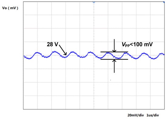
Figure 6.
The voltage ripple waveform under a rated input voltage of 48 V.
The parameters of the GaN-based hard-switching full-bridge converter designed in this study are presented in Table 2.
Table 2.
Specifications of the prototype.
Figure 7a shows the transient response of the converter under a 48 V input voltage when the load transitions from no-load to full-load, with a response time of approximately 200 µs. Figure 7b illustrates the transient response under the same input voltage when the load transitions from full-load to no-load, with a response time of approximately 100 µs. The figures demonstrate the rapid transient response of the converter, which is attributed to the use of GaN transistors. The high switching frequency enabled by GaN transistors increases the bandwidth of the closed-loop system, thereby improving the dynamic performance of the converter.
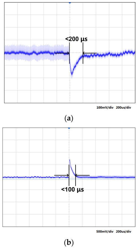
Figure 7.
Measured output voltage waveform under a 48 V input with varying load conditions. (a) Load transition from no load to full load; (b) Load transition from full load to no load.
Table 3 presents a performance comparison between the prototype developed in this study and those from other laboratories. Compared to existing studies, the prototype in this paper demonstrates a significant advantage in output power. Furthermore, the peak efficiency and full-load efficiency of this design surpass those reported in other works, while also exhibiting a notably high power density. These comparisons highlight the advantages of the proposed GaN-based power converter in terms of both efficiency and compactness.
Table 3.
Performance summary and comparison with the state-of-the art.
4. Conclusions
This paper presents a hard-switching full-bridge converter based on GaN transistors, utilizing a full-bridge topology on the primary side and a full-wave rectification circuit with synchronous rectification on the secondary side. The operating principle of the main power circuit is thoroughly analyzed, and a prototype is constructed for experimental validation. Experimental results demonstrate that the GaN-based hard-switching full-bridge converter achieves a significant improvement in efficiency, with a peak efficiency of 97.1%, outperforming conventional converters by over 2%. The use of GaN transistors enables higher switching frequencies, effectively reducing the size of the output filter and achieving a power density of 430 W/in3. Furthermore, the increased switching frequency enhances the bandwidth of the closed-loop system, improving the dynamic response of the power module. The integration of GaN transistors not only enhances the efficiency but also increases the power density of the converter. The proposed prototype offers a solution to meet the stringent size and efficiency requirements of the power supply for renewable energy solutions, automotive, aerospace, and communication power supplies.
Author Contributions
Conceptualization, F.M. and X.W.; methodology, F.M. and X.W.; software, X.W.; validation, X.W.; writing—original draft preparation, X.W. and Q.Z.; writing—review and editing, F.M. and Z.Z.; supervision, F.M.; project administration, X.W. All authors have read and agreed to the published version of the manuscript.
Funding
This work was supported in part by the National Key Research and Development Program Project of China under Project 2023YFB4403200 and in part by the National Natural Science Foundation of China under Project U21A20459.
Data Availability Statement
The original contributions presented in this study are included in this article. Further inquiries can be directed to the corresponding author.
Conflicts of Interest
Xin Wang was employed by the company China Electronics Technology Group Corporation. The remaining authors declare that the research was conducted in the absence of any commercial or financial relationships that could be construed as a potential conflict of interest.
References
- Rojas-Dueñas, G.; Riba, J.-R.; Moreno-Eguilaz, M. A Deep Learning-Based Modeling of a 270 V-to-28 V DC-DC Converter Used in More Electric Aircrafts. IEEE Trans. Power Electron. 2022, 37, 509–518. [Google Scholar] [CrossRef]
- Shahzad, D.; Farooq, M.; Pervaiz, S.; Afridi, K.K. A High-Power-Density High-Efficiency Soft-Switched Single-Phase Universal Input to 28-V Isolated AC–DC Converter Module Designed for Paralleled Operation. IEEE Trans. Power Electron. 2022, 37, 8262–8280. [Google Scholar] [CrossRef]
- Shah, F.M.; Xiao, H.M.; Li, R.; Awais, M.; Zhou, G.; Bitew, G.T. Comparative performance evaluation of temperature dependent characteristics and power converter using GaN, SiC and Si power devices. In Proceedings of the 2018 IEEE 12th International Conference on Compatibility, Power Electronics and Power Engineering (CPE-POWERENG 2018), Doha, Qatar, 10–12 April 2018. [Google Scholar]
- Liao, X.; Wang, Y.; Zeng, C.; Li, R.; Chen, Y.; Lai, P.; Huang, Y.; En, Y. Investigation of high-temperature-reverse-bias (HTRB) degradation on AlGaN/GaN HEMTs. In Proceedings of the 2014 IEEE International Conference on Electron Devices and Solid-State Circuits (EDSSC), Chengdu, China, 18–20 June 2014; pp. 1–2. [Google Scholar]
- Chen, H.-Y.; Lin, W.T.; Liao, C.H.; Lin, Z.Y.; Zhang, Z.Q.; Kao, Y.Y.; Chen, K.H.; Lin, Y.H.; Lin, S.R.; Tsai, T.Y. A domino bootstrapping 12 V GaN driver for driving an on-chip 650 V eGaN power switch for 96% high efficiency. In Proceedings of the 2020 IEEE Symposium on VLSI Circuits, Honolulu, HI, USA, 16–19 June 2020; pp. 1–2. [Google Scholar]
- Kao, Y.-Y.; Hung, S.H.; Chen, H.Y.; Lee, J.J.; Chen, K.H.; Lin, Y.H.; Lin, S.R.; Tsai, T.Y. Fully integrated GaN-on-silicon gate driver and GaN switch with temperature-compensated fast turn-on technique for achieving switching frequency of 50 MHz and slew rate of 118.3 V/Ns. IEEE J. Solid-State Circuits 2021, 56, 3619–3627. [Google Scholar] [CrossRef]
- Lin, S.-Y.; Lin, S.Y.; Hung, S.H.; Wang, T.W.; Li, C.H.; Go, C.L.; Huang, S.C.; Chen, K.H.; Zheng, K.L.; Lin, Y.H.; et al. A GaN gate driver with on-chip adaptive on-time controller and negative current slope detector. In Proceedings of the 2023 IEEE International Solid-State Circuits Conference (ISSCC), San Francisco, CA, USA, 19–23 February 2023; pp. 306–308. [Google Scholar]
- Choi, J.; Tsukiyama, D.; Tsuruda, Y.; Davila, J.M.R. High-frequency, high-power resonant inverter with eGaN FET for wireless power transfer. IEEE Trans. Power Electron. 2018, 33, 1890–1896. [Google Scholar] [CrossRef]
- Yan, D.; Ma, D.B. An automotive-use battery-to-load GaN-based switching power converter with anti-aliasing MR-SSM and in-cycle adaptive ZVS techniques. IEEE J. Solid-State Circuits 2021, 56, 1186–1196. [Google Scholar] [CrossRef]
- Yeh, C.-H.; Lin, Y.T.; Kuo, C.C.; Huang, C.J.; Xie, C.Y.; Lu, S.F.; Yang, W.H.; Chen, K.H.; Liu, K.C.; Lin, Y.H. A 70W and 90% GaN-based class-E wireless-powertransfer system with automatic-matching-point-search control for zerovoltage switching and zero-voltage-derivative switching. In Proceedings of the 2018 IEEE International Solid-State Circuits Conference-(ISSCC), San Francisco, CA, USA, 11–15 February 2018; pp. 138–140. [Google Scholar]
- Yang, T.-H.; Wen, Y.H.; Chiu, C.K.; Chen, K.H.; Lin, Y.H.; Lin, S.R.; Tsai, T.Y. A pre-charge tracking technique in the 40 MHz high-speed switching 48-to-5 V GaN-based DC–DC buck converter for reducing large self-commutation loss and achieving a high efficiency of 95.4%. IEEE J. Solid-State Circuits 2022, 57, 2045–2053. [Google Scholar] [CrossRef]
- Chen, Y.; Ma, D.B. A 10-MHz closed-loop EMI-regulated GaN switching power converter using emulated Miller Plateau tracking and adaptive strength gate driving. IEEE J. Solid-State Circuits 2021, 56, 531–540. [Google Scholar] [CrossRef]
- Sebastian, J.; Fernandez, A.; Villegas, P.; Hernando, M.; Prieto, M.J. New topologies of active input current shapers to allow AC-to-DC converters to comply with the IEC-1000-3-2. In Proceedings of the 31st Annual Power Electronics Specialists Conference. Conference Proceedings, Galway, Ireland, 23 June 2000; Volume 2, pp. 565–570. [Google Scholar]
- Kondrath, H. Investigation into Component Losses and Efficiency of a Bidirectional Full-Bridge DC-DC Converter. In Proceedings of the IECON 2018—44th Annual Conference of the IEEE Industrial Electronics Society, Washington, DC, USA, 21–23 October 2018; pp. 1273–1278. [Google Scholar]
- Khodabakhsh, J.; Moschopoulos, G. A Comparative Study of Conventional and T-Type ZVS-PWM Full-Bridge Converters. In Proceedings of the 2018 IEEE Energy Conversion Congress and Exposition (ECCE), Portland, OR, USA, 23–27 September 2018; pp. 6314–6319. [Google Scholar]
- Gu, B.; Lai, J.-S.; Kees, N.; Zheng, C. Hybrid-Switching Full-Bridge DC–DC Converter with Minimal Voltage Stress of Bridge Rectifier, Reduced Circulating Losses, and Filter Requirement for Electric Vehicle Battery Chargers. IEEE Trans. Power Electron. 2013, 28, 1132–1144. [Google Scholar] [CrossRef]
- Bhargavi, P.; Chaganti, P.C.V.; Sowmya, V.; Manitha, P.V.; Lekshmi, S. A Comparative study of Phase shifted Full Bridge and High-Frequency Resonant Transistor DC-DC Converters for EV Charging Application. In Proceedings of the 2022 IEEE 2nd International Conference on Mobile Networks and Wireless Communications (ICMNWC), Tumkur, Karnataka, India, 2–3 December 2022; pp. 1–6. [Google Scholar]
- Lim, C.-Y.; Jeong, Y.; Moon, G.-W. Phase-Shifted Full-Bridge DC–DC Converter with High Efficiency and High Power Density Using Center-Tapped Clamp Circuit for Battery Charging in Electric Vehicles. IEEE Trans. Power Electron. 2019, 34, 10945–10959. [Google Scholar] [CrossRef]
- Wu, H.; Mu, T.; Ge, H.; Xing, Y. Full-Range Soft-Switching-Isolated Buck-Boost Converters with Integrated Interleaved Boost Converter and Phase-Shifted Control. IEEE Trans. Power Electron. 2016, 31, 987–999. [Google Scholar] [CrossRef]
- Landon, T.; Steinbeiser, C.; Page, P.; Hajji, R.; Burgin, G.; Branson, R.; Krutko, O.; Delaney, J.; Witkowski, L. Design of a 600W Doherty using generation 2 HVHBT with 55% WCDMA efficiency linearized to −55dBc for 2c11 6.5dB PAR. In Proceedings of the 2012 IEEE Topical Conference on Power Amplifiers for Wireless and Radio Applications, Santa Clara, CA, USA, 15–18 January 2012; pp. 73–76. [Google Scholar]
- Steinbeiser, C.; Page, P.; Landon, T.; Burgin, G. Doherty Power Amplifiers Using 2nd Generation HVHBT Technology for High Efficiency Basestation Applications. In Proceedings of the 2010 IEEE Compound Semiconductor Integrated Circuit Symposium (CSICS), Monterey, CA, USA, 3–6 October 2010; pp. 1–4. [Google Scholar]
- Takenaka, I.; Ishikura, K.; Takahashi, H.; Hasegawa, K.; Ueda, T.; Kurihara, T.; Asano, K.; Iwata, N. A 330W Distortion-Cancelled Doherty 28V GaAs HJFET Amplifier with 42% Efficiency for W-CDMA Base Stations. In Proceedings of the 2006 IEEE MTT-S International Microwave Symposium Digest, San Francisco, CA, USA, 11–16 June 2006; pp. 1344–1347. [Google Scholar]
- Chandrashekar, K.; Ashwini, U. Dual Channel C-Band Solid State Power Amplifier for Unmanned Aerial Vehicles. In Proceedings of the 2024 International Microwave and Antenna Symposium (IMAS), Marrakech, Morocco, 21–23 October 2024; pp. 1–5. [Google Scholar]
- Gagan, M.N.; Usha, A.; Jagadeesh, S.; Singh, B.K.; Chippalkatti, V.S. Design and implementation of pulsed output interleaved flyback converter with lossless snubber and current mode control. In Proceedings of the 2017 International Conference on Smart grids, Power and Advanced Control Engineering (ICSPACE), Bangalore, India, 17–19 August 2017; pp. 53–58. [Google Scholar]
- Dragon, C.; Brakensiek, W.; Burdeaux, D.; Burger, W.; Funk, G.; Hurst, M.; Rice, D. 200W push-pull & 110W single-ended high performance RF-LDMOS transistors for WCDMA basestation applications. In Proceedings of the IEEE MTT-S International Microwave Symposium Digest, 2003, Philadelphia, PA, USA, 8–13 June 2003; Volume 1, pp. 69–72. [Google Scholar]
- Noh, G.; Lim, G.C.; Ha, J.I. Analysis of Synchronous-Rectification Switch Control for Active Class-E Rectifier. In Proceedings of the 2021 IEEE Energy Conversion Congress and Exposition (ECCE), Vancouver, BC, Canada, 10–14 October 2021; pp. 2059–2066. [Google Scholar]
- Shen, J.; Jing, L.; Qiu, J. High-frequency Full-bridge 48V DC-5V DC LLC Resonant Converter with AlGaN/GaN HEMTs. In Proceedings of the 2023 5th International Conference on Electrical Engineering and Control Technologies (CEECT), Chengdu, China, 15–17 December 2023; pp. 338–342. [Google Scholar]
- Zambetti, O.; Colombo, M.; D’angelo, S.; Saggini, S.; Rizzolatti, R. 48V to 12V isolated resonant converter with digital controller. In Proceedings of the 2017 IEEE Applied Power Electronics Conference and Exposition (APEC), Tampa, FL, USA, 26–30 March 2017; pp. 315–321. [Google Scholar]
- Li, M.; Ouyang, Z.; Andersen, M.A.E. A Hybrid Multitrack-Sigma Converter with Integrated Transformer for Wide Input Voltage Regulation. In Proceedings of the 2020 IEEE Applied Power Electronics Conference and Exposition (APEC), New Orleans, LA, USA, 15–19 March 2020; pp. 1844–1850. [Google Scholar]
- Fu, M.; Fei, C.; Yang, Y.; Li, Q.; Lee, F.C. A Two-Stage Rail Grade DC/DC Converter Based on GaN Device. In Proceedings of the 2019 IEEE Applied Power Electronics Conference and Exposition (APEC), Anaheim, CA, USA, 17–21 March 2019; pp. 2110–2114. [Google Scholar]
Disclaimer/Publisher’s Note: The statements, opinions and data contained in all publications are solely those of the individual author(s) and contributor(s) and not of MDPI and/or the editor(s). MDPI and/or the editor(s) disclaim responsibility for any injury to people or property resulting from any ideas, methods, instructions or products referred to in the content. |
© 2025 by the authors. Licensee MDPI, Basel, Switzerland. This article is an open access article distributed under the terms and conditions of the Creative Commons Attribution (CC BY) license (https://creativecommons.org/licenses/by/4.0/).