Article

A Sub-1-V Nanopower MOS-Only Voltage Reference

1
Institute of VLSI Design, Zhejiang University, Hangzhou 310027, China
2
School of Electronics and Information, Soochow University, Suzhou 215123, China
3
Beijing Smartchip Microelectronics Technology Co., Ltd., Beijing 102200, China
*
Author to whom correspondence should be addressed.
J. Low Power Electron. Appl. 2024, 14(1), 13; https://doi.org/10.3390/jlpea14010013
Submission received: 29 December 2023 / Revised: 26 January 2024 / Accepted: 27 February 2024 / Published: 29 February 2024
(This article belongs to the Special Issue Ultra-Low-Power ICs for the Internet of Things Vol. 2)

Abstract

:
A novel low-power MOS-only voltage reference is presented. The Enz–Krummenacher–Vittoz (EKV) model is adopted to provide a new perspective on the operating principle. The normalized charge density, introduced as a new variable, serves as an indicator when trimming the output temperature coefficient. The proposed voltage reference consists of a specific current generator and a 5-bit trimmable load. Thanks to the good match between the current source stage and the output stage, the nonlinear temperature dependence of carrier mobility is automatically canceled out. The circuit is designed using 55 nm COMS technology. The operating temperature ranges from −40 ° C to 120 ° C. The average temperature coefficient of the output voltage can be reduced to 21.7 ppm/ ° C by trimming. The power consumption is only 23.2 nW with a supply voltage of 0.8 V. The line sensitivity and the power supply rejection ratio at 100 Hz are 0.011 %/V and −89 dB, respectively.

1. Introduction

The low-power voltage reference is an essential circuit block in power-limited applications, such as the Internet of Things (IoT), portable devices, and biological interfaces [1,2,3,4,5]. As a constant reference quantity for the circuit system, the robustness and insensitivity of its output have crucial impacts on the performance of the system. The voltage reference in such applications aims to keep a stable and constant output in any process, voltage, and temperature (PVT) with minimal power.
Currently, voltage reference sources can be roughly sorted into three categories: bipolar (BJT) references, CMOS references, and hybrid references. The traditional bipolar bandgap references (BGRs) generate an output voltage of about 1.2 V ( V B G ), which is relatively consistent among different process technologies. Despite that BGR has little process variation, it requires a supply voltage higher than 1 V [6,7,8]. This is not suitable for most low-power applications and is not available in some advanced technology nodes. Furthermore, the temperature coefficient (TC) of the conventional first-order BGR is relatively large. Meanwhile, high-order compensation technology inevitably makes the circuit topology more complex.
To realize a voltage reference operating with a sub-1 V supply, the latter two references have been developed [9,10,11,12,13,14]. The CMOS references are generally based on the temperature characteristics of the threshold voltage ( V T ). The V T -based references (VTR) utilize the exponential relationship of MOS transistors biased in the subthreshold region to take the place of BJTs. The output voltage of VTRs is usually equal to the extrapolated value of the threshold voltage, thus allowing the lower supply voltage. Unfortunately, the process variation of its output voltage is larger compared to that of BGR. Some VTRs also need resistors to generate a controllable voltage proportional to the absolute temperature (PTAT) [15,16,17]. Because the current is limited to very small, it can be seen that the resistor not only costs more mask layers in manufacturing but also occupies more chip area. In addition, some designs associate the different types of transistors [1,18,19], generating an output proportional to the difference of two threshold values ( V T 1 V T 2 ). Although this technique can significantly reduce the supply voltage, it also requires the use of more masks and increases the process variations.
Recently, some works combined the principles of VTR and BGR, creating a hybrid voltage reference [20,21,22]. The hybrid reference generates a nominal value of V B G V T with process dependence compensated by a dimension-induced side-effect. However, reducing the minimum supply voltage of the hybrid reference is challenging because of the fixed voltage drop between the base and emitter.
Based on the analyses above, we present a new VTR that only consists of one type of MOS transistor. A novel current source is proposed and discussed by a new approach. A simple trimming method is also adopted to further reduce the TC. The paper is organized as follows. Section 2 reviews the basic EKV model, and introduces it into the explanation of the principle of V T -based voltage reference. Section 3 presents the design of the proposed circuit and shows the detailed design considerations of each part. Section 4 gives the simulated results and the comparison with other works that have been reported in recent years. Section 5 concludes the paper.

2. Principle of MOS-Only Voltage Reference

2.1. EKV Model

Before we look into the Enz–Krummenacher–Vittoz (EKV) model, it is admirable to revisit the conventional square-law model, which is widely adopted in textbooks. For saturation region and triode region, the drain current equation I D of the square-law model can be expressed as follows:
I D = μ C ox W L V GS V TH V DS 1 2 V DS 2 ,
where μ is the carrier mobility, C o x is the gate oxide capacitance of unit area, W is the width of the MOS transistor, L is the length of the MOS transistor, and V G S and V D S are, respectively, the gate and drain voltage referred to the source terminal. It is important to note that, to distinguish it from V T , V T H is the threshold voltage with respect to the source. It can be seen from Equation (1) that the thermal voltage U T is not taken into account, which leads to the poor coherence between the equation and simulation in temperature-dependent performance. As a circuit module that is highly concerned with temperature characteristics, when designing and analyzing the voltage reference, the model should include a comprehensive representation of temperature characteristics. Thus, we introduce the Enz–Krummenacher–Vittoz (EKV) model to explain and optimize the proposed voltage reference circuit.
The EKV model is a charge-based compact model proposed by Enz, Krummenacher, and Vittoz in Switzerland in 1995 [23]. The starting point of this model was to establish a single equation that could adapt to all inversion regions [24,25,26,27]. The drain current I D of the EKV model is expressed through the normalized drain current i [28,29]:
i = I D I S ,
where I S is the specific current, defined as
I S = 2 n U T 2 μ C o x W L = 2 n U T 2 μ C o x K .
Here, n is the subthreshold slope factor of the MOS transistor, which varies between 1.3 and 2, depending on the process technology. K is called the aspect ratio. It can be seen that the temperature dependence of I S depends on the carrier mobility and thermal voltage. The temperature dependence of the mobility can be expressed as μ = μ ( T R ) · ( T / T R ) m , where the range of m is 1.5 to 2 [30]. Hence, the specific current is a nonlinear increasing function of temperature, approximately proportional to T 2 m .
The basic EKV model introduces a new variable q x , called normalized mobile charge density, to value the amount of charge density at the location x along the channel. The normalized mobile charge density can be calculated from the nonequilibrium voltage V x along the channel as follows:
V P V x = U T [ 2 ( q x 1 ) + ln ( q x ) ] ,
V P = V G V T n ,
where V T and V G are the bulk-referenced threshold voltage and gate voltage, respectively, and V P is defined as the pinch-off voltage. Equation (4) represents the relationship between the V x and q x at the location x. We can replace the subscript of x with S or D to obtain the charge density at the source or drain terminal. When we obtain the q S and q D based on the source and drain voltage, the normalized drain current of the transistor i can be derived as follows:
i = ( q S 2 + q S ) ( q D 2 + q D ) .
On the right side of Equation (6), the square term q 2 represents drift current, which is proportional to the surface potential strength. The linear term q represents diffusion current, which is proportional to the mobile charge density gradient. The part inside the first bracket is called forward current, and the part inside the second bracket is called reverse current. Equation (6) is applicable to both saturated and nonsaturated transistors. However, for saturated transistors, where the V D is greater than the pinch-off voltage V P , the current contributed by the second bracket can be neglected.
Above are the basic equations of the EKV model. For the origin of Equations (4)–(6), we provide a detailed derivation in Appendix A. It is admirable that the EKV model provides predictions of MOSFET behavior across all operating regions, including weak inversion, moderate inversion, and strong inversion. In addition, q not only represents the normalized charge density but also can serve as an index of channel inversion level. When q << 1, that is, q > q 2 , the diffusion current is dominant. At this point, the channel is in weak inversion (WI). Similarly, when q >> 1, the channel is in strong inversion (SI). When q = 1, the drift current is equal to the diffusion current, and the channel is in moderate inversion (MI).

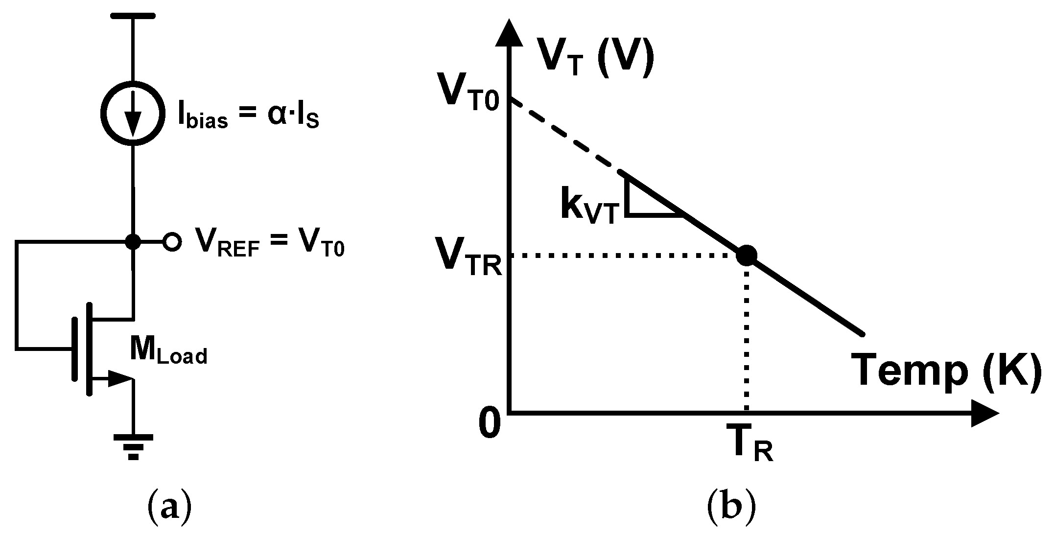
2.2. MOS-Only Voltage Reference Operation Principle

The basic principle of V T -based voltage reference is to bias a diode-connected MOSFET with a definite current that varies with temperature. The conceptual diagram is shown in Figure 1a, and the following text details the analysis of how to determine the magnitude and the temperature dependence of this current.
As shown in Figure 1b, the threshold voltage V T is complementary to the absolute temperature (CTAT) with good linearity. Thus its temperature dependence can be represented by a linear function:
V T = V T 0 k V T T ,
where k V T is the temperature coefficient (positive value), and V T 0 is the intersection when the line is extrapolated to absolute zero temperature.
According to Equations (4) and (5), the gate voltage for a source-grounded MOSFET can be expressed as follows:
V G = n U T [ 2 ( q S 1 ) + ln ( q S ) ] + V T .
The first term of Equation (8) is PTAT, and the second term is CTAT. In other words, to make the gate voltage a temperature-independent quantity V R E F , the temperature coefficients of the two terms must complement each other.
n k b e 0 [ 2 ( q S 1 ) + ln ( q S ) ] = k V T ,
where k b is the Boltzmann constant, e 0 is the elementary charge. Unfortunately, Equation (9) does not have an analytical solution, but we can use the function ω ( x ) to represent the solution of the equation y + ln ( y ) = x . ω ( x ) can be found in the Symbolic Math Toolbox of MATLAB R2018a or newer versions as a mathematical function w r i g h t O m e g a . Therefore, q S can be expressed as follows:
q S = 1 2 ω ( k V T k b / e 0 + 2 + ln 2 ) .
Assuming the transistor is saturated, we eliminate the reverse current by combining Equations (2), (6) and (10), and it can be determined that the required bias current I b i a s is
I b i a s = I S · 1 4 ω 2 ( k V T k b / e 0 + 2 + ln 2 ) = α I S ,
where α is a positive dimensionless constant. As shown in Equation (11), the quantity in the parentheses is temperature-independent, i.e., α is temperature-independent. Therefore, the temperature characteristic of the required bias current is consistent with the temperature characteristic of I S . At this bias current, the gate voltage of the diode-connected transistor M L o a d is equal to V T 0 . It should be noted that the drain voltage of M L o a d is also V T 0 ; thus, the assumption of saturation holds.
Through the analysis above, we can see that the key of V T -based voltage reference is to generate a current exactly proportional to the specific current I S of the load transistor. It is worth noting that when q S deviates from our expected value, the right side of Equation (8) introduces a temperature-dependent term. In other words, the target bias current biases the load transistor to a constant inversion level. Interestingly, the temperature characteristic of carrier mobility does not appear in the analysis above. This is because as long as the bias current is proportional to the specific current, the nonlinear temperature dependence of μ is automatically canceled out.

3. Circuit Design

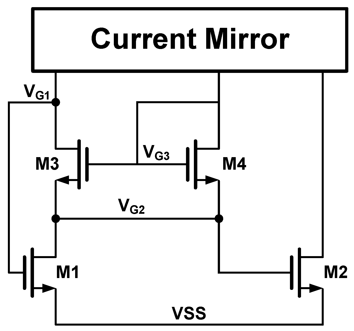
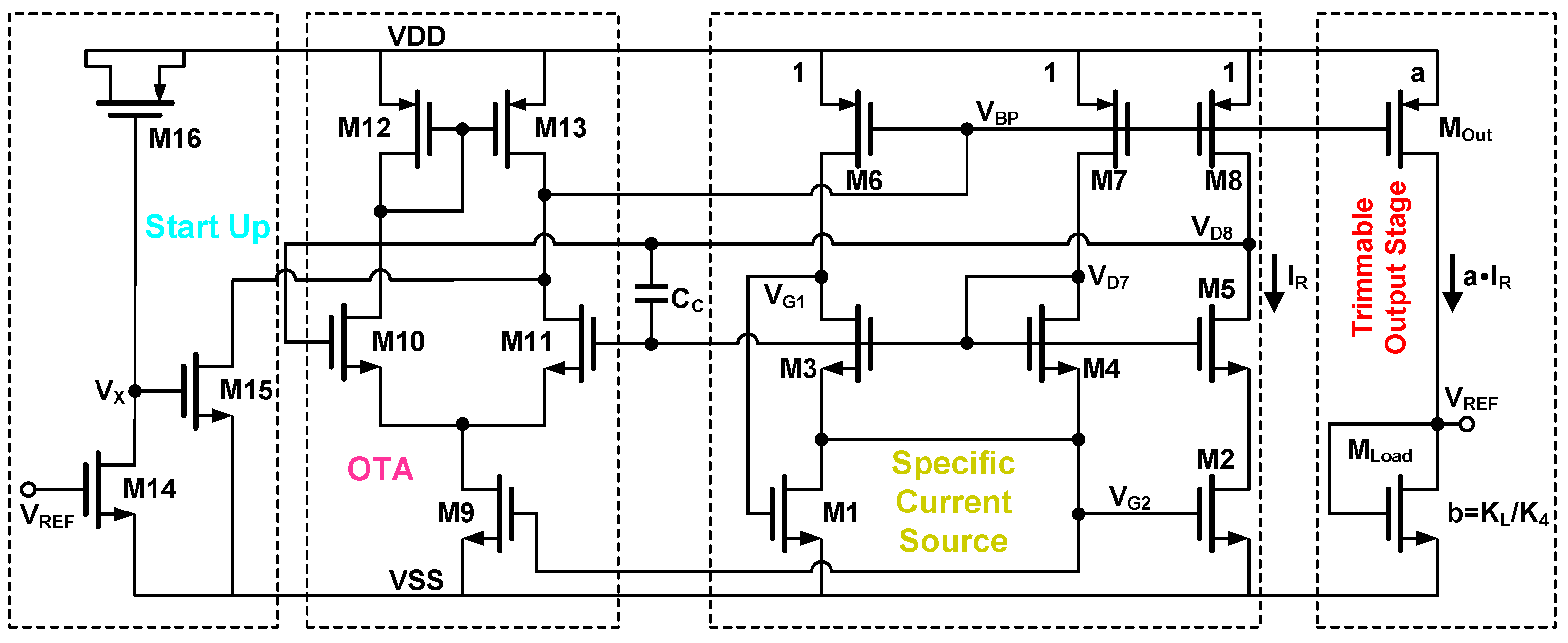
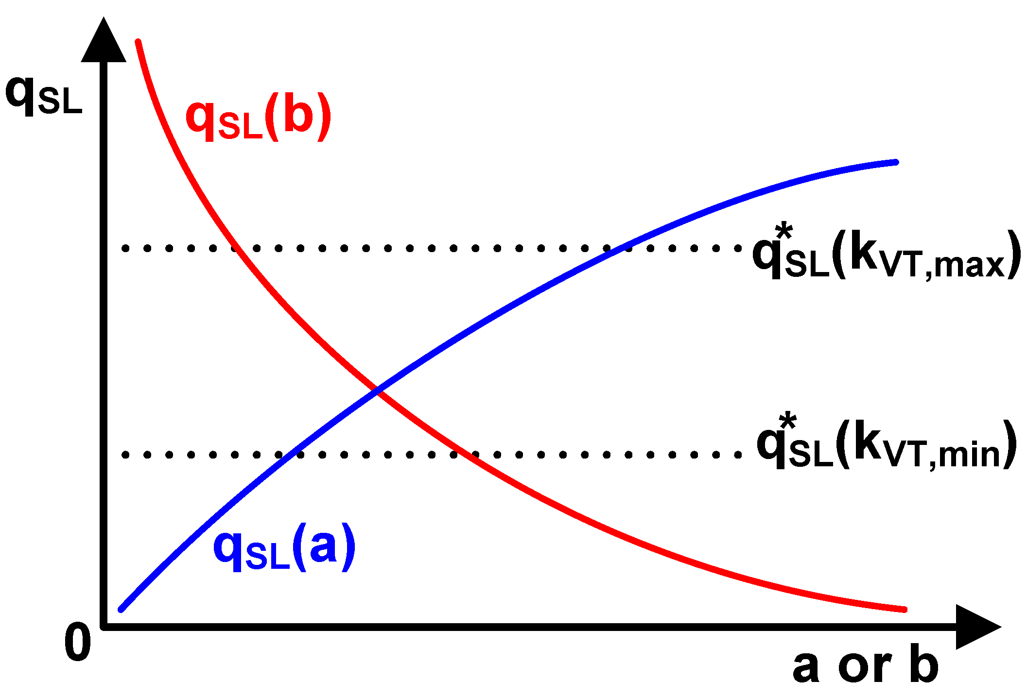
3.1. Proposed Specific Current Source
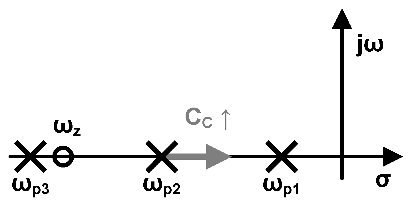
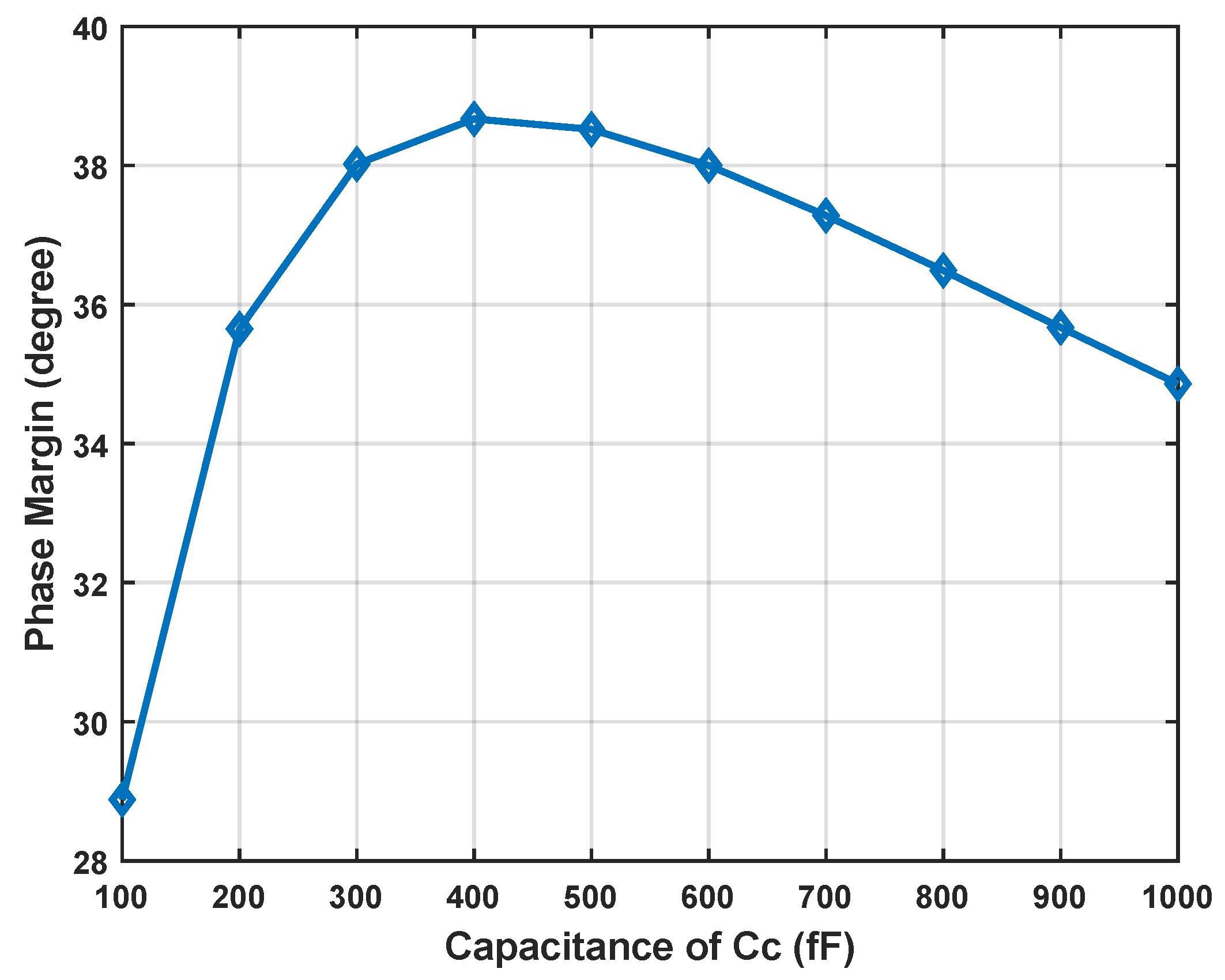
Just as we concluded in Section 2.2, the key of the V T -based voltage reference is to design a specific current source. The core circuit of the proposed specific current source is shown in Figure 2. The devices in the circuit determining the current are M 1 M 4 . To ensure that the current generated matches the load transistor M L o a d , the unit size of M 1 M 4 is equal to the size of M L o a d . In other words, to avoid V T mismatch caused by inconsistent channel lengths, all NMOS transistors have identical unit sizes to eliminate the impact of second-order effects. In addition, the bulk terminals of all NMOS are connected to V S S .
The current mirror in the upper part of Figure 2 could be replaced by either a simple PMOS current mirror or a cascoded one. For ease of explaining its operating principle, we assume that the current ratios of these three branches are equal. Thus, the drain currents of M 1 M 4 can be expressed as follows:
1 2 i 1 I S 1 = i 2 I S 2 = i 3 I S 3 = i 4 I S 4 = I R .
For each transistor, we can use Equations (4) and (6) to sequentially derive out the following relationships:
M 1 : V P 1 = U T 2 + ln q S 1 = V G 1 V T n i 1 = q S 1 = 2 I R I S 1 ;
M 2 : V P 2 = U T 2 + ln q S 2 = V G 2 V T n i 2 = q S 2 = I R I S 2 ;
M 3 : V P 3 V G 2 = U T 2 ( q S 3 1 ) V P 3 V G 1 = U T 2 ( q D 3 1 ) i 3 = q S 3 2 q D 3 2 = I R I S 3 ;
M 4 : V P 4 V G 2 = U T 2 ( q S 4 1 ) i 4 = q S 4 2 = I R I S 4 .
The equations listed above were simplified based on the proper assumptions as follows: (i) The sizes of M 1 and M 2 are set large enough, thus, the q 1 , 2 = I D 1 , 2 / I S 1 , 2 1 . (ii) The sizes of M 3 and M 4 are set small enough, thus, the q 3 , 4 = I D 3 , 4 / I S 3 , 4 1 . Simply speaking, M 1 , 2 are in weak inversion level, and M 3 , 4 are in strong inversion level. If we set the sizes of the M 1 and M 2 to be similar, the difference between V G 1 and V G 2 can be controlled at a lower level. In other words, M 3 is in the deep triode region, while M 1 , 2 , 4 is in saturation. In Equations (13), (14) and (16), therefore, we neglected the contribution of q D 1 , 2 , 4 to the normalized drain current.
By combining Equations (13) and (14), we have the following:
V G 1 V G 2 = n U T ln ( 2 I S 2 I S 1 ) .
Since V P 3 is equal to V P 4 , we can easily determine that q S 3 and q S 4 are equal. When we take the difference of the first two rows of Equation (15), we can obtain another relationship of V G 1 and V G 2 :
V G 1 V G 2 = 2 U T ( q S 3 q D 3 ) .
The third row of Equation (15) can also be written as follows:
q S 3 2 q D 3 2 = I R I S 3 = q S 4 2 · I S 4 I S 3 = q S 3 2 · I S 4 I S 3 .
By substituting Equation (17) into Equation (18), we will have a quadratic equation of q S 3 :
q S 3 2 ( q S 3 c 1 ) 2 = q S 3 2 · c 2 ,
where c 1 = 1 2 n ln ( 2 I S 2 / I S 1 ) , and c 2 = I S 4 / I S 3 . Finally, we can obtain the solution of Equation (20), and the produced current can be expressed as follows:
q S 3 = c 1 c 2 ( 1 + 1 c 2 ) = q S 4 ,
I R = q S 4 2 · I S 4 = c 1 2 c 2 2 ( 1 + 1 c 2 ) 2 · I S 4 .
The other root of Equation (20) is discarded, as it does not comply with the assumption made before, that q S 3 , D 3 1 . If we substitute c 1 and c 2 with the aspect ratios of M 1 M 4 , Equation (22) can be rewritten as follows:
I R = 1 2 μ U T 2 C o x n 3 ln 2 ( 2 K 2 K 1 ) · K 3 2 K 4 1 + 1 K 4 K 3 2 .
Therefore, the current of each branch is proportional to the specific current. The temperature characteristic of I R also follows the characteristic of the unit transistor.
The complete schematic of the proposed voltage reference is given in Figure 3. As annotated in the figure, the overall circuit is composed of four parts: a specific current source, an operational transconductance amplifier (OTA), a start-up circuit, and a trimmable output stage. A cascode transistor M 5 is added to mitigate the difference in drain voltage between M 1 and M 2 . The OTA is used to decrease the voltage difference of V D 7 and V D 8 , thus, improving the accuracy of the current mirror and reducing the line sensitivity. The role of the start-up circuit is to help the circuit to reach the desired stable state after power-up. Finally, the output stage copies the I R and generates the reference voltage V R E F . In the following subsection, we will give detailed explanations of the operating principles of the remaining part.

3.2. Loop Stability

While the amplifier enhances the loop gain, at the same time, the stability of the loop needs to be carefully analyzed. Thus, to prevent the parasitic oscillation of the circuit, a compensation capacitor C C is added.
The proposed specific current source contains three branches, and both positive feedback and negative feedback exist in the loop. Thus, the expression of the total loop gain is quite complex. Based on reasonable simplifications and comparison with simulation, the frequency response of the loop gain can be expressed as follows:
L G ( s ) = K s w z s w p 1 s w p 2 s w p 3 ,
where
w z = g m 1 C g s 2 ; w p 1 = w o t a = g o t a C o t a ; w p 2 = g d s p C c 1 + g m 2 g m 1 + g m 2 g m 3 g m 4 g d s 3 ; w p 3 = g m 2 C g s 2 · ( 1 + g m 1 g m 2 + g m 1 g d s 3 ) ; L G ( 0 ) = g m p g d s p · g m 2 g d s 3 · ( 1 g m 3 g m 4 ) · g m o t a g o t a .
L G ( 0 ) is the DC gain of the loop. g o t a and C o t a denote the conductance and capacitance at the output node of the amplifier. The loop gain contains one negative zero and three negative poles. w p 1 and w p 2 are much smaller than w p 3 , contributing a phase shift of 180 ° . Given that the current in M 1 is twice that of M 2 , g m 1 / g m 2 is approximately equal to 2. Hence, w p 3 is larger than the zero w z , causing the phase to increase by 90 ° and then decrease by 90 ° . The distribution of the loop’s poles and zero is shown in Figure 4. As the compensating capacitance C C increases, w p 2 moves towards the origin. By carefully locating two poles, w p 1 2 , it is possible to retain enough phase margin. The detailed stability results will be presented in the section on simulation results.

3.3. Output Stage

After generating the required current I R , we can copy it into the load transistor with a certain proportion and obtain a reference voltage approximately equal to V T 0 . Due to the variation of V T and its temperature coefficient during the actual manufacturing, it is necessary to perform trimming in the output branch. As follows, two methods of trimming will be presented: (i) trimming the multiplier of M L o a d ; (ii) trimming the copy ratio of the current mirror.
If we suppose the copy ratio of the PMOS current mirror is 1 : a , and the aspect ratio of the load transistor is K L , then
q S L = a K 4 K L · q s 4 = c 1 c 2 ( 1 + 1 c 2 ) · a b ,
where b = K L / K 4 . According to Equation (10), the trimming range determined by the variables a and b must cover the variations in k V T caused by the process corner. The effects of a and b on the normalized charge density of M L o a d are shown in Figure 5. If we increase the output stage current, i.e., a, the normalized charge density of the load q S L will rise. When it reaches the value calculated from Equation (10), the temperature coefficient of the V R E F approximates zero. Similarly, adjusting the size of the load transistor, i.e., b, can achieve the same goal.
The dashed line represents the target charge density, where the temperature coefficient should be zero. q S L * ( k V T , m a x ) corresponds to the case of a relatively large k V T , and, similarly, the q S L * ( k V T , m i n ) does, too. Hence, the intersection points of two dashed lines and q S L ( a ) , or q S L ( b ) , indicate the minimum trimming range.

3.4. Start-Up Circuit

When the power supply voltage is applied, all branches in the voltage reference may remain zero. Thus, a start-up circuit formed by M 14 M 16 is adopted to assist the circuit escape from the zero-current state [31].
In the initial start-up stage, due to V R E F being zero, M 14 is turned off. Therefore, the ramp-up of VDD is coupled to node V S T through the MOS capacitor M 16 . Once the voltage of V S T exceeds the threshold voltage of M 15 , the node V B P will be pulled down, hence the branch current rising. Meanwhile, V R E F will also rise until it reaches the final steady state. When V R E F becomes the desired value, approximately V T 0 , M 14 is turned on, discharging the node V S T to ground. Finally, M 15 is turned off, disconnecting the start-up circuit from the core circuit.

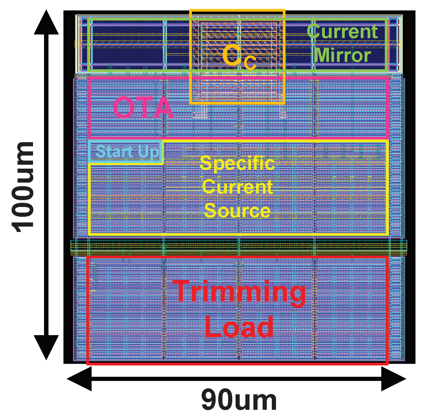
4. Simulation Results

In the early stage of circuit design, we use the EKV model to investigate the behavior of the circuit and roughly determine the size of the transistor. The parameters of the EKV model can be extracted through simulation using a MATLAB script which is available on the website provided in [29]. To ensure the simulation accuracy, the final results are still obtained through the Spectre simulator with the BSIM4 model. Table 1 gives the sizes of each transistor in Figure 3.

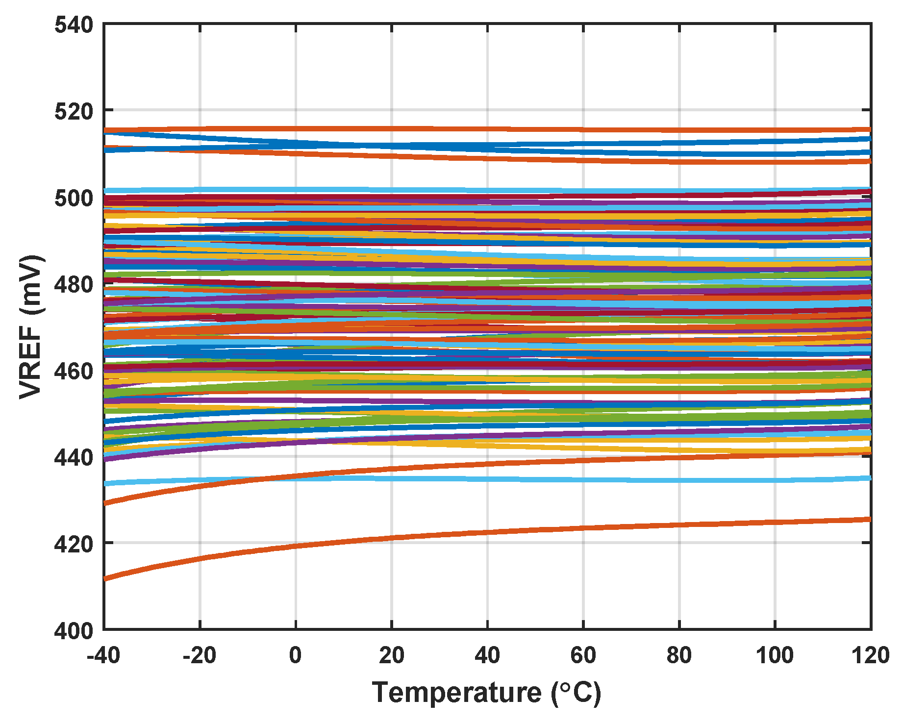
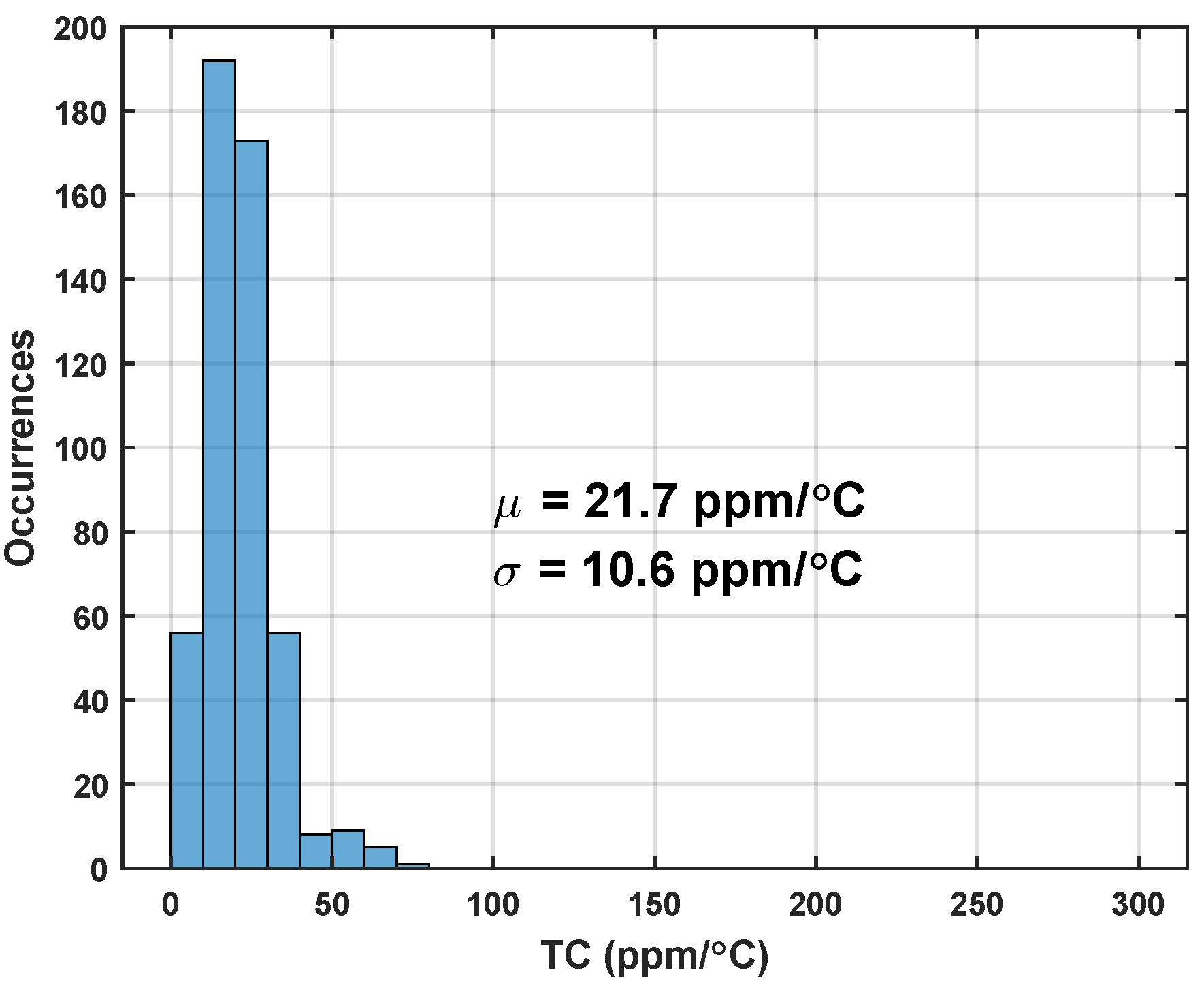
4.1. Temperature Dependence before Trimming

As explained in Section 3.3, we can trim the temperature coefficient by adjusting the size of the load transistor or the current mirror ratio. It is preferred to take the method of trimming load, thus the consumption of the circuit can be constant. The total current consumption of the proposed voltage reference is proportional to the specific current of the unit NMOS transistor. According to Equation (3), the power of the circuit is approximately a PTAT quantity. At room temperature, the generated specific current I R is 3.6 nA. As we set the output current ratio a equal to 3, the total current is approximately 8 times that of I R , i.e., 29.0 nA. Across the entire temperature range, the total current increases from 19.3 nA at −40 ° C to 41.2 nA at 120 ° C.
In order to determine the trimming range of the circuit, it is necessary to evaluate the temperature dependence before trimming. A Monte Carlo simulation of 500 samples is performed, sweeping the temperature from −40 ° C to 120 ° C. Both mismatch and corner variation are included in the model to ensure the performance after layout. To avoid making the figure too cluttered, only 100 V R E F curves are shown in Figure 6. Thanks to the fact that the specific current of M L o a d is well matched to the current generated, curves before trimming are relatively flat. The average value of V R E F varies from 421 mV to 522 mV. Figure 7 shows the TC histogram of 500 samples. The mean of TC is about 41.8 ppm/ ° C, and the standard deviation is about 37.0 ppm/ ° C. The statistical distribution indicates that the temperature coefficient of the vast majority of samples is less than 100 ppm/ ° C, which can be easily reduced through trimming.

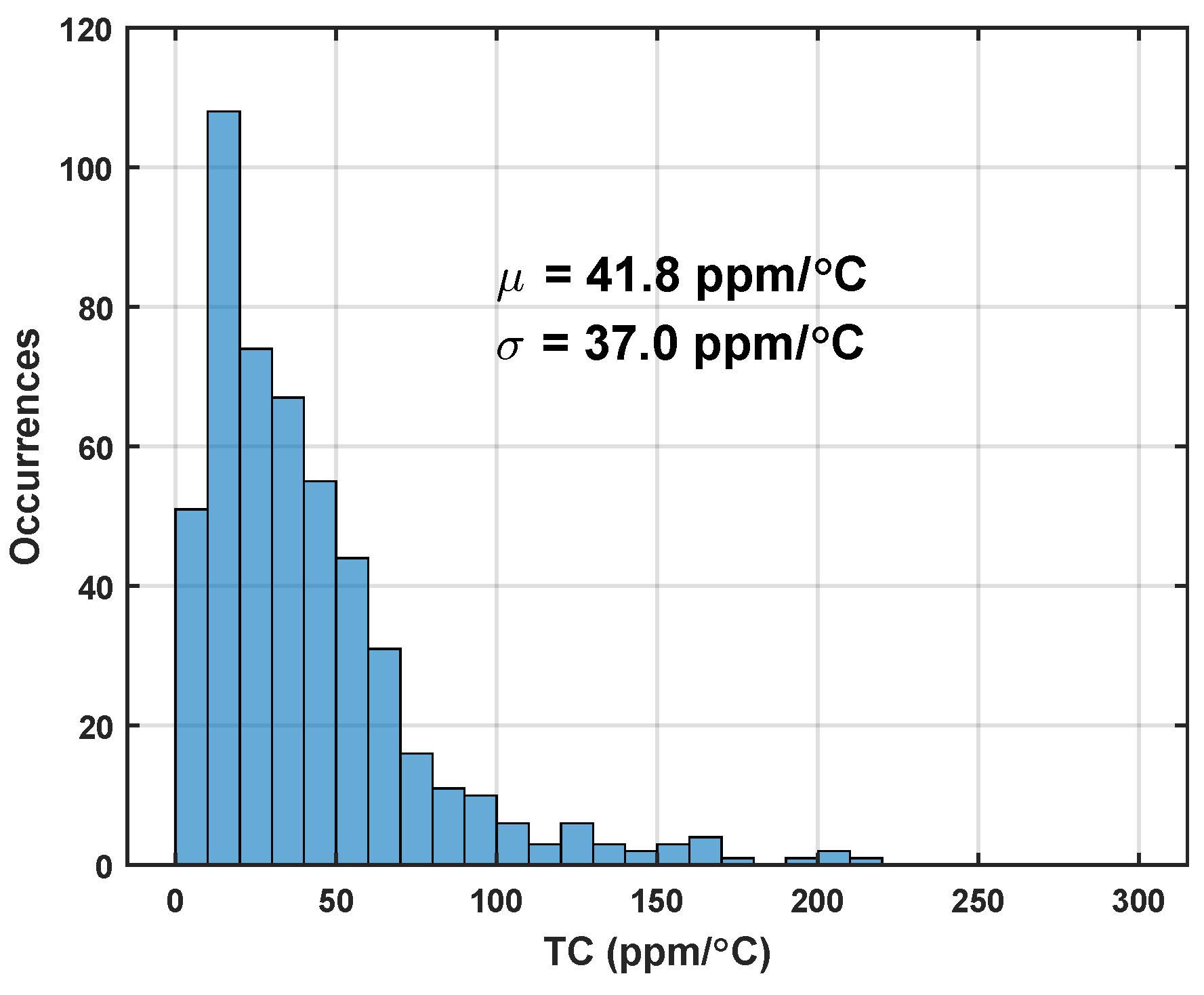
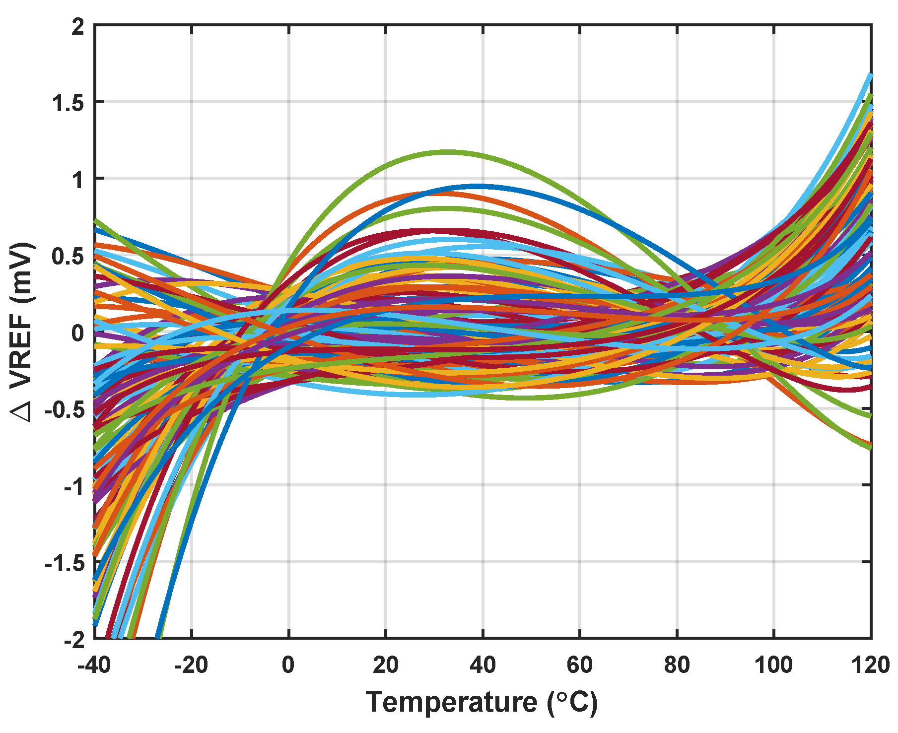
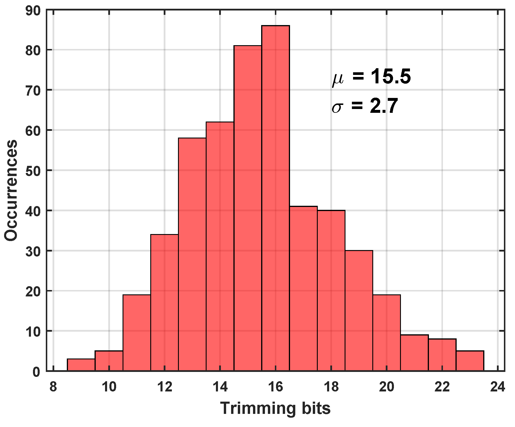
4.2. Temperature Dependence after Trimming

The process variation range of V T 0 is relatively wide, as Figure 6 confirms. Therefore, we cannot use the one-point trimming methodology as BJT-based voltage reference does. The trimming method we adopted can be described as follows: (1) Sweep the trim bits at one ambient temperature, e.g., 20 ° C, to obtain the voltage of V R E F . (2) Sweep the trim bits at another ambient temperature, e.g., 60 ° C, to obtain another set of output values. (3) Take the absolute difference between two sets of data. The trim bits corresponding to the minimum difference are the final bits we need.
A single NMOS switch is used to connect or disconnect the variable load transistors to the output. The size of the variable load follows a binary order, specifically, 1, 1/2, 1/4, 1/16, and 1/32, with respect to the size of M L o a d . Similarly, we performed a Monte Carlo simulation of 500 samples with the above trimming procedure. Figure 8 presents the trimmed output voltage after subtracting its mean value. The curves intersect at the two temperature points where we performed the trimming. The histogram in Figure 9 shows that the mean of TC is reduced to 21.7 ppm/ ° C and the standard deviation to 10.6 ppm/ ° C. A total of 84.2 percent of the samples have a temperature coefficient below 30 ppm/ ° C, and 95.4 percent of the samples have a temperature coefficient below 40 ppm/ ° C.
After calibration, the distribution of average output voltage and the final determined trimming bits are shown in Figure 10 and Figure 11. The mean value of the V R E F is 474.4 mV, roughly similar to the output under the typical process corner. As we adopted the global Monte Carlo model during simulation, the variation coefficient σ / μ is 5.8%, which is larger compared to the coefficient of BGR. V R E F is relatively higher under the fast corner and lower under the slow corner; therefore, the proposed voltage reference can also serve as an indicator of the NMOS corner. Figure 11 implies that the selection of a 5-bit trimming range can meet the needs of the vast majority of samples. The bits number varies from 9 to 23, and its mean value is around the half of 2 5 .

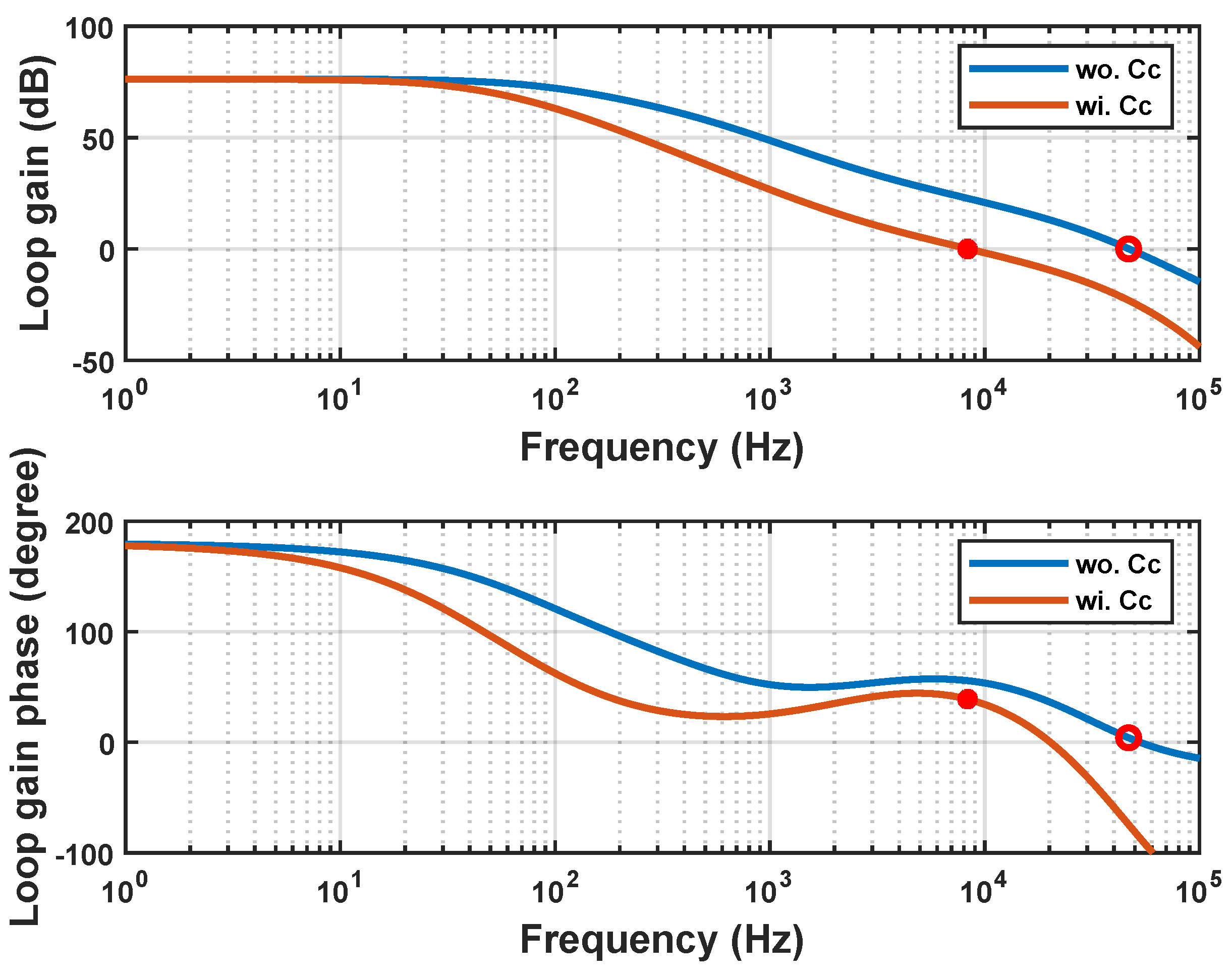
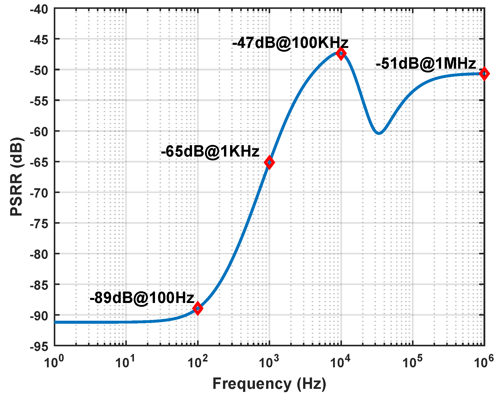
4.3. Frequency Compensation

Figure 12 illustrates the frequency response of the loop gain with or without C C . The red circles in the figure denote the unit gain frequency and the corresponding phase margin. As explained in Section 3.2, the increasing of C C compresses the unity gain bandwidth of the loop. When the unity gain bandwidth decreases, the frequency point corresponding to the phase margin first approaches w p 3 and then moves closer to w z . In a figurative sense, the corresponding point will first climb a hill and then descend into a valley. The simulation result of phase margin versus C C is shown in Figure 13. The capacitance value of the C C is finally determined to be 400 fF, while the phase margin of the loop is 38.7 ° .

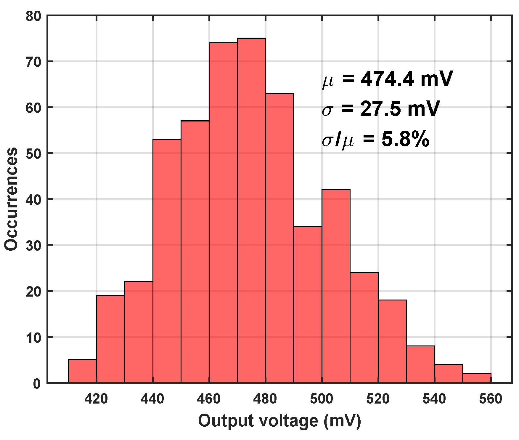
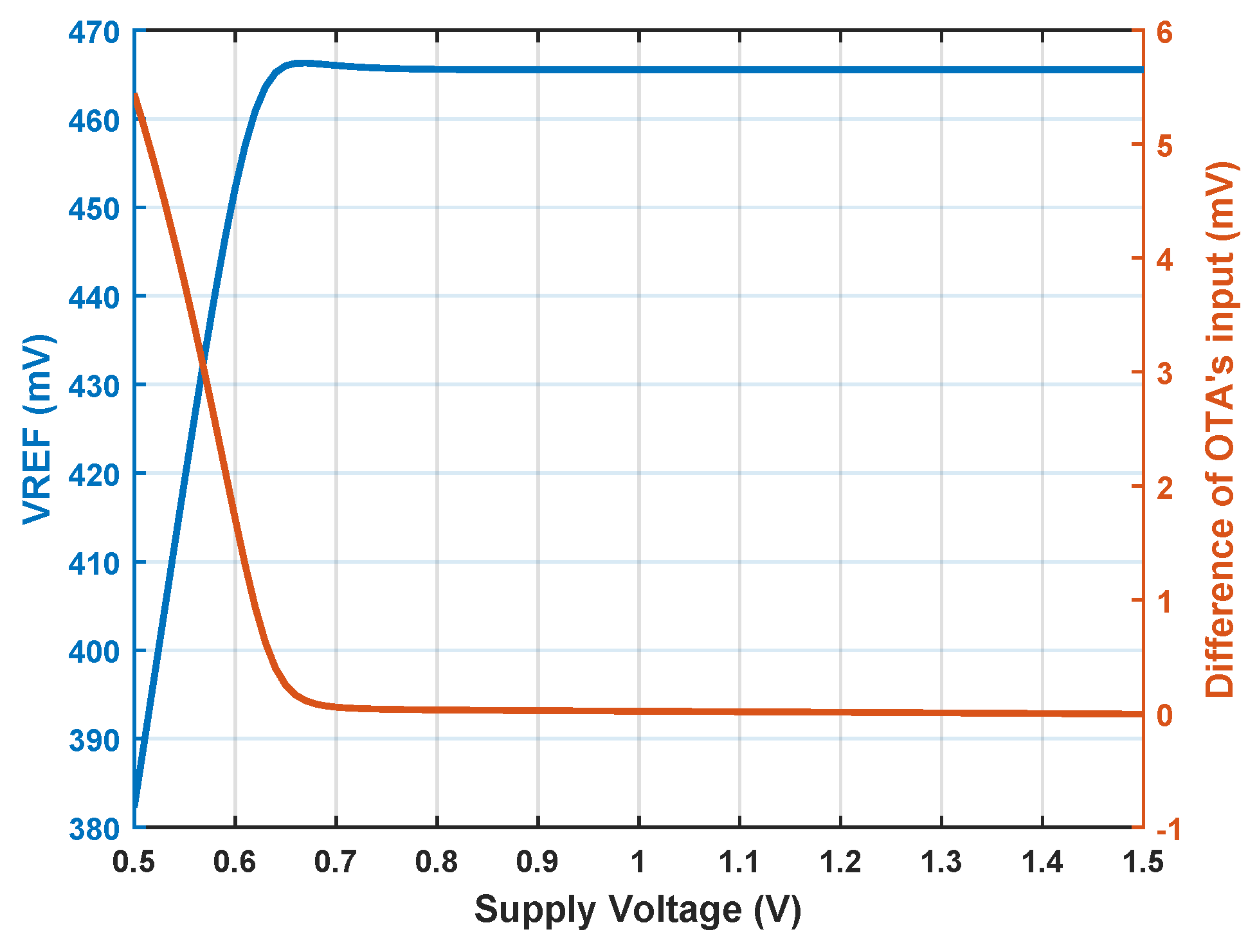
4.4. Supply Dependence

The supply dependence of the proposed voltage reference was simulated at room temperature. Figure 14 shows the output voltage and the input difference of the amplifier as functions of VDD. The minimum supply voltage could be as low as 0.8 V, and the line sensitivity (LS) is 0.011%, ranging from 0.8 V to 1.5 V. The maximum supply voltage is mainly limited by the breakdown voltage of V D S . The results also indicate that a lower supply voltage leads to inaccuracy in the specific current generator. The acceptable supply voltage depends not only on the voltage headroom of the PMOS current mirror but also on the allowable amplifier input residue, because the larger the residue, the worse the temperature coefficient of V R E F . Figure 15 shows the power supply rejection ratio (PSRR) with a load capacitance of 10 pF at room temperature. Thanks to the additional amplifier, the PSRR is −89 dB at 100 Hz.
Figure 16 shows the layout of the proposed voltage reference. Each part of the circuit is annotated, including the compensation capacitor C C . The overall area of the core circuit is only 90 µm × 100 µm. Since the size of all NMOS is determined based on the unit cell M u , the layout of the circuit is highly compact. C C is composed of a metal–insulator–metal (MIM) capacitor using top metal; thus, it can be stacked on the active device to save area. Dummy transistors are added on both sides of the layout to mitigate the layout-dependent effect (LDE).
Table 2 compares the performance of the proposed V T -based voltage reference with other reported works. It can be seen that the proposed reference is very competitive in many aspects. We balanced the circuit’s power and TC, adding an amplifier to improve LS with an acceptable current consumption. Thus, our design shows excellent supply and temperature independence. Meanwhile, our design only adopts one type of MOSFET, which makes it more efficient in terms of mask layer numbers and process portability. Compared with [32], which also contains one MOSFET type, our design achieves a lower supply voltage and less power consumption. In addition, our design enables the majority of chips to achieve a small TC through a 5-bit trimming, which improves the yield in practical system applications.

5. Conclusions

This paper presents a 55 nm low-power V T -based voltage reference. The reference proposed only requires MOS transistors, and no BJTs or resistors are needed. A detailed explanation of the operating principle and design of the circuit was given with the EKV model. The reference consists of a novel specific current generator, a simple amplifier, a start-up circuit, and a trimmable output stage.
The simulation results showed that a balanced trade-off between TC and power was achieved. The proposed voltage reference has an average TC of 21.7 ppm/ ° C with a power consumption of 23.2 nW. The circuit also has excellent supply independence. Its line sensitivity is only 0.011 %/V, and PSRR is −89 dB at 100 Hz. The core area of the circuit is 0.009 mm 2 . Therefore, the proposed circuit is a suitable voltage reference module for low-power applications.

Author Contributions

Conceptualization, S.W.; methodology, S.W.; validation, S.W.; writing—original draft, S.W.; writing—review and editing, Z.L. and X.Y.; supervision, K.X.; project administration, H.D. and Z.W. All authors have read and agreed to the published version of the manuscript.

Funding

This work was supported by the National Key Research and Development Program of China under Grant SQ2022YFB3200085.

Data Availability Statement

All data are available from the authors upon request.

Conflicts of Interest

Authors Kunpeng Xu, Hongguang Dai and Zhanxia Wu were employed by the company Beijing Smartchip Microelectronics Technology Co., Ltd. The remaining authors declare that the research was conducted in the absence of any commercial or finacial relationships that could be construed as a potential conflict of interest.

Appendix A

In this appendix, the origins of basic EKV equations are derived. Firstly, there are two transport mechanisms in the composition of the MOS transistor: drift current and diffusion current. The total drain current I D can be expressed as follows:
I D = μ W Q i d ψ S d x + U T d Q i d x ,
where Q i is the mobile charge density, and ψ S is the surface potential at the position x along the channel. The diffusion factor varies little across the WI, MI, and SI. Therefore, for diffusion current, the relationship between Q i and surface potential can be approximated as follows:
d Q i C o x = 1 + γ 2 ψ S d ψ S = n d ψ S ,
where γ is known as the back gate parameter. We normalize the Q i as follows:
q = Q i 2 n U T C o x ,
Thus, Equation (A2) can be expressed as follows:
d ψ S = 2 U T d q .
Therefore, we rewrite the differential equation of the drain current:
S D I D d x = S D 2 n U T 2 C o x ( 2 q + q ) d q .
Finally, we perform the integration from the source terminal to the drain terminal and obtain
I D = 2 n U T 2 μ C o x W L · q S 2 + q S q D 2 + q D .
Another fundamental physical equation of the EKV model relates the nonequilibrium voltage V and q:
Q i exp ψ S ϕ F V U T ,
hence,
d Q i Q i = d q q = d ψ S d V U T .
Substituting Equation (A4) into Equation (A8), we obtain
q x q P 2 + 1 q d q = V x V P 1 U T d V .
where q P denotes the normalized charge density at the pinch-off point and equals one. Thus, we connect the V and q after integration and have Equation (4).
The physical interpretation of the linear relationship between V P and V G is relatively complex, and due to text space constraints, the detailed derivation is not provided here. Readers can find a detailed explanation of Equation (5) in reference [23,28].

References

  1. Wang, J.; Sun, X.; Cheng, L. A Picowatt CMOS Voltage Reference Operating at 0.5-V Power Supply with Process and Temperature Compensation for Low-Power IoT Systems. IEEE Trans. Circuits Syst. II Express Briefs 2023, 70, 1336–1340. [Google Scholar] [CrossRef]
  2. Parisi, A.; Finocchiaro, A.; Papotto, G.; Palmisano, G. Nano-Power CMOS Voltage Reference for RF-Powered Systems. IEEE Trans. Circuits Syst. II Express Briefs 2018, 65, 1425–1429. [Google Scholar] [CrossRef]
  3. Zhu, Z.; Hu, J.; Wang, Y. A 0.45 V, Nano-Watt 0.033% Line Sensitivity MOSFET-Only Sub-Threshold Voltage Reference with No Amplifiers. IEEE Trans. Circuits Syst. I Regul. Pap. 2016, 63, 1370–1380. [Google Scholar] [CrossRef]
  4. Yan, W.; Li, W.; Liu, R. Nanopower CMOS Sub-Bandgap Reference with 11 ppm/°C Temperature Coefficient. Electron. Lett. 2009, 45, 627. [Google Scholar] [CrossRef]
  5. Zhang, H.; Liu, X.; Zhang, J.; Zhang, H.; Li, J.; Zhang, R.; Chen, S.; Carusone, A.C. A Nano-Watt MOS-Only Voltage Reference with High-Slope PTAT Voltage Generators. IEEE Trans. Circuits Syst. II Express Briefs 2018, 65, 1–5. [Google Scholar] [CrossRef]
  6. Kim, M.; Cho, S. A Single BJT Bandgap Reference with Frequency Compensation Exploiting Mirror Pole. IEEE J. Solid-State Circuits 2021, 56, 2902–2912. [Google Scholar] [CrossRef]
  7. Zhang, Z.; Zhan, C.; Wang, L.; Law, M.K. A −40 °C–125 °C 0.4-µA Low-Noise Bandgap Voltage Reference with 0.8-mA Load Driving Capability Using Shared Feedback Resistors. IEEE Trans. Circuits Syst. II Express Briefs 2022, 69, 4033–4037. [Google Scholar]
  8. Huang, W.; Liu, L.; Zhu, Z. A Sub-200nW All-in-One Bandgap Voltage and Current Reference without Amplifiers. IEEE Trans. Circuits Syst. II Express Briefs 2021, 68, 121–125. [Google Scholar] [CrossRef]
  9. Vita, G.D.; Iannaccone, G. A Sub-1 V, 10 ppm/°C, Nanopower Voltage Reference Generator. In Proceedings of the 2006—32nd European Solid-State Circuits Conference, Montreaux, Switzerland, 19–21 September 2006; pp. 307–310. [Google Scholar]
  10. Ueno, K.; Hirose, T.; Asai, T.; Amemiya, Y. A 300 nW, 15 ppm/°C, 20 ppm/V CMOS Voltage Reference Circuit Consisting of Subthreshold MOSFETs. IEEE J. Solid-State Circuits 2009, 44, 2047–2054. [Google Scholar] [CrossRef]
  11. Qiao, H.; Zhan, C.; Chen, Y. A −40 °C to 140 °C Picowatt CMOS Voltage Reference with 0.25-V Power Supply. IEEE Trans. Circuits Syst. II Express Briefs 2021, 68, 3118–3122. [Google Scholar] [CrossRef]
  12. Aminzadeh, H. All–MOS Self-Powered Subthreshold Voltage Reference with Enhanced Line Regulation. AEU Int. J. Electron. Commun. 2020, 122, 153245. [Google Scholar] [CrossRef]
  13. Luong, P.; Christoffersen, C.; Rossi-Aicardi, C.; Dualibe, C. Nanopower, Sub-1 V, CMOS Voltage References with Digitally-Trimmable Temperature Coefficients. IEEE Trans. Circuits Syst. I Regul. Pap. 2017, 64, 787–798. [Google Scholar] [CrossRef]
  14. De Lima, V.F.; Klimach, H. A 37 nW MOSFET-Only Voltage Reference in 0.13 µm CMOS. In Proceedings of the 2020 33rd Symposium on Integrated Circuits and Systems Design (SBCCI), Campinas, Brazil, 24–28 August 2020; pp. 1–6. [Google Scholar]
  15. Che, C.; Lei, K.M.; Martins, R.P.; Mak, P.I. A 0.4-V 8400-µm2 Voltage Reference in 65-nm CMOS Exploiting Well-Proximity Effect. IEEE Trans. Circuits Syst. II Express Briefs 2023, 70, 3822–3826. [Google Scholar]
  16. Parisi, A.; Finocchiaro, A.; Palmisano, G. An accurate 1-V threshold voltage reference for ultra-low power applications. Microelectron. J. 2017, 63, 155–159. [Google Scholar] [CrossRef]
  17. Fan, H.; Fang, Z.; Li, Y.; Qian, Q.; Kang, X.; Chen, M.; Sun, W. A 3.38-ppm/°C Voltage Reference for Harsh Environment Applications Empowered by the In-Loop Resistance Trimming Technique. IEEE Trans. Circuits Syst. II Express Briefs 2023. early access. [Google Scholar] [CrossRef]
  18. Navidi, M.M.; Graham, D.W. A Low-Power Voltage Reference Cell with a 1.5 V Output. J. Low Power Electron. Appl. 2018, 8, 19. [Google Scholar] [CrossRef]
  19. Seok, M.; Kim, G.; Blaauw, D.; Sylvester, D. A Portable 2-Transistor Picowatt Temperature-Compensated Voltage Reference Operating at 0.5 V. IEEE J. Solid-State Circuits 2012, 47, 2534–2545. [Google Scholar] [CrossRef]
  20. Ji, Y.; Lee, J.; Kim, B.; Park, H.J.; Sim, J.Y. 18.8 A 192pW Hybrid Bandgap-Vth Reference with Process Dependence Compensated by a Dimension-Induced Side-Effect. In Proceedings of the 2019 IEEE International Solid-State Circuits Conference (ISSCC), San Francisco, CA, USA, 17–21 February 2019; pp. 308–310. [Google Scholar]
  21. Liu, X.; Liang, S.; Liu, W.; Sun, P. A 2.5 ppm/°C Voltage Reference Combining Traditional BGR and ZTC MOSFET High-Order Curvature Compensation. IEEE Trans. Circuits Syst. II Express Briefs 2021, 68, 1093–1097. [Google Scholar] [CrossRef]
  22. Chowdary, G.; Kota, K.; Chatterjee, S. A 1-nW 95-ppm/°C 260-mV Startup-Less Bandgap-Based Voltage Reference. In Proceedings of the 2020 IEEE International Symposium on Circuits and Systems (ISCAS), Seville, Spain, 12–14 October 2020; pp. 1–4. [Google Scholar]
  23. Enz, C.C.; Krummenacher, F.; Vittoz, E.A. An analytical MOS transistor model valid in all regions of operation and dedicated to low-voltage and low-current applications. Analog Integr. Circuits Signal Process. 1995, 8, 83–114. [Google Scholar] [CrossRef]
  24. Enz, C.; Chicco, F.; Pezzotta, A. Nanoscale MOSFET Modeling: Part 1: The Simplified EKV Model for the Design of Low-Power Analog Circuits. IEEE Solid-State Circuits Mag. 2017, 9, 26–35. [Google Scholar] [CrossRef]
  25. Enz, C.; Chicco, F.; Pezzotta, A. Nanoscale MOSFET Modeling: Part 2: Using the Inversion Coefficient as the Primary Design Parameter. IEEE Solid-State Circuits Mag. 2017, 9, 73–81. [Google Scholar] [CrossRef]
  26. Enz, C.; Chalkiadaki, M.A.; Mangla, A. Low-power analog/RF circuit design based on the inversion coefficient. In Proceedings of the ESSCIRC Conference 2015—41st European Solid-State Circuits Conference (ESSCIRC), Graz, Austria, 14–18 September 2015; IEEE: New York, NY, USA, 2015; pp. 202–208. [Google Scholar]
  27. Enz, C.; Pezzotta, A. Nanoscale MOSFET modeling for the design of low-power analog and RF circuits. In Proceedings of the 2016 MIXDES—23rd International Conference Mixed Design of Integrated Circuits and Systems, Lodz, Poland, 23–25 June 2016; IEEE: New York, NY, USA, 2016; pp. 21–26. [Google Scholar]
  28. Jespers, P. The gm/ID Methodology, a Sizing Tool for Low-Voltage Analog CMOS Circuits: The Semi-Empirical and Compact Model Approaches; Springer Science & Business Media: New York, NY, USA, 2009. [Google Scholar]
  29. Jespers, P.G.A.; Murmann, B. Systematic Design of Analog CMOS Circuits: Using Pre-Computed Lookup Tables; Cambridge University Press: Cambridge, UK, 2017. [Google Scholar]
  30. Filanovsky, I.; Allam, A. Mutual compensation of mobility and threshold voltage temperature effects with applications in CMOS circuits. IEEE Trans. Circuits Syst. I Fundam. Theory Appl. 2001, 48, 876–884. [Google Scholar] [CrossRef]
  31. Alhasssan, N.; Zhou, Z.; Sánchez Sinencio, E. An All-MOSFET Sub-1-V Voltage Reference with a—51-dB PSR up to 60 MHz. IEEE Trans. Very Large Scale Integr. (VLSI) Syst. 2017, 25, 919–928. [Google Scholar] [CrossRef]
  32. Chen, Y.; Guo, J. A 42nA IQ, 1.5–6V VIN, Self-Regulated CMOS Voltage Reference with −93 dB PSR at 10 Hz for Energy Harvesting Systems. IEEE Trans. Circuits Syst. II Express Briefs 2021, 68, 2357–2361. [Google Scholar] [CrossRef]
Figure 1. (a) The conceptual diagram of V T -based voltage reference; (b) the temperature characteristic of V T .
Jlpea 14 00013 g001
Figure 2. Core circuit of the proposed specific current source.
Jlpea 14 00013 g002
Figure 3. Schematic of the proposed V T -based voltage reference source.
Jlpea 14 00013 g003
Figure 4. Pole-zero plot of loop gain and the effect of compensating capacitor.
Jlpea 14 00013 g004
Figure 5. The impact of a (current mirror copy ratio) and b (size ratio K L / K 4 ) on the normalized charge density of M L o a d .
Jlpea 14 00013 g005
Figure 6. Monte Carlo simulation results before trimming: temperature dependence of V R E F .
Jlpea 14 00013 g006
Figure 7. Monte Carlo simulation results before trimming: histogram of temperature coefficient.
Jlpea 14 00013 g007
Figure 8. Monte Carlo simulation results after trimming: temperature dependence of Δ V R E F .
Jlpea 14 00013 g008
Figure 9. Monte Carlo simulation results after trimming: histogram of temperature coefficient.
Jlpea 14 00013 g009
Figure 10. Histogram of average output voltage after trimming.
Jlpea 14 00013 g010
Figure 11. Histogram of determined trimming bits number.
Jlpea 14 00013 g011
Figure 12. Frequency response of loop gain without or with C C .
Jlpea 14 00013 g012
Figure 13. Phase margin as a function of C C .
Jlpea 14 00013 g013
Figure 14. V R E F and difference of OTA’s input voltage versus supply voltage.
Jlpea 14 00013 g014
Figure 15. PSRR with a C L of 10 pF.
Jlpea 14 00013 g015
Figure 16. Layout.
Figure 16. Layout.
Jlpea 14 00013 g016
Table 1. Sizes of the transistors in Figure 3.
TransistorSizeTransistorSize
M u 0.12/20 (µm/µm) M 10 , 11 4 M u
M 1 64 M u M 12 , 13 5/20 (µm/µm)
M 2 52 M u M 14 2 M u
M 3 3 M u M 15 2 M u
M 4 , 5 1 M u M 16 5/20 (µm/µm)
M 6 8 5/20 (µm/µm) M O u t 3 × 5/20 (µm/µm)
M 9 104 M u M L o a d ( 1 4 47 64 ) M u
Table 2. Comparison of the proposed voltage reference with previous works.
ParameterThis WorkTCASII’23 [1]TCASII’23 [15]TCASII’21 [32]SBCCI’20 [14]JLPEA’18 [18]
Process (nm)5518065180130350
Temp. Range (°C)−40–120−10–100−20–80−40–85−40–125−70–85
TC (ppm/°C)21.79079.460.8628.842
V R E F (mV)474.4288107.2985575.21520
σ / μ (%)5.80.5742.42.64.322
Supply (V)0.8–1.50.5–20.4–0.81.5–61–1.81.7–3.3
LS (%/V)0.0110.230.540.0030.07110
Consumption (nW)23.20.556.76336.41110
PSRR (dB)−89 (@100 Hz)−45 (@100 Hz)−66.5 (@10 Hz)−93.3 (@10 Hz)−54.4 (@100 Hz)−35 (@100 Hz)
Area (mm2)0.0090.00290.00840.0150.00780.06
Components1 Type MOS3 Types MOSMOS + Res2 Types MOS1 Type MOS2 Types MOS + Res
Disclaimer/Publisher’s Note: The statements, opinions and data contained in all publications are solely those of the individual author(s) and contributor(s) and not of MDPI and/or the editor(s). MDPI and/or the editor(s) disclaim responsibility for any injury to people or property resulting from any ideas, methods, instructions or products referred to in the content.

