Abstract
HfO2 thin films are extensively applied in optical coatings and microelectronic devices. However, film defects, which are vital to the performance of the thin films, are still under intense investigation. In this work, the absorption, photoluminescence, and crystallization characteristics of HfO2 films prepared by electron-beam evaporation and ion-assisted deposition are investigated in detail. Experimental results showed that high-temperature thermal annealing in air resulted in a reduced absorption coefficient, an increased bandgap width, and an increased degree of crystallization. After thermal annealing, an absorption shoulder near 5.8 eV was caused by excitons in the films, which were independent of oxygen vacancy defects and crystallization. Under 6.4 eV (193 nm) laser excitation, the photoluminescence spectrum showed five emission peaks for HfO2 films both with and without thermal annealing. The emission peak near 4.4 eV was generated by the self-trapped exciton, and the peak near 4.0 eV was related to the OH group in the film. The oxygen vacancy defect-induced absorption of HfO2 films in a broad spectral range significantly increased when HfO2 film was re-annealed in Ar gas after first being annealed in air, while the photoluminescence spectrum showed no significant change, indicating that the emission peaks at 2.3, 2.8, and 3.4 eV were not related to oxygen vacancy defects.
1. Introduction
HfO2 is a dielectric material with a wide band-gap, high dielectric constant, high refractive index, and high thermal stability that is widely used in the preparation of optical coatings and microelectronic films [1,2,3]. For optical thin-film applications, it is widely used in the preparation of optical films with low absorption and high damage threshold for high-power pulsed laser systems [4,5,6,7,8]. For microelectronic applications, HfO2 is the most promising alternative to SiO2 in metal-oxide-semiconductor (MOS) microelectronic devices [9]. Studies have shown that there are various defects in HfO2 films, such as oxygen vacancies and charge traps [9,10,11,12,13,14,15,16]. These defects affect the absorption loss and laser damage threshold of the optical coatings, and the leakage current and carrier mobility of the MOS. The investigation of the defects in HfO2 films is therefore of great significance for the preparation of high-performance laser optical thin films and microelectronic films.
Defects in HfO2 films are difficult to measure directly. When defects are present, localized states are generated between the valence band and conduction band. When electrons at lower energy levels absorb photon energy, they may jump to higher energy levels, and when electrons at higher energy levels return back to lower energy levels via radiation relaxation, photon emission may occur. Therefore, the optical absorption spectrum and the photoluminescence emission spectrum of HfO2 films can be used to analyze the defect states in the films. There has been some past research studying both the absorption and photoluminescence of HfO2 optical films. Ciapponi et al. found that HfO2 films prepared by electron-beam deposition (EBD) showed significant luminescence, but the luminescence of ion-assisted films could not be distinguished from the uncoated substrate [15]. Papernov et al. studied the optical properties of oxygen vacancies in HfO2 thin films by absorption and luminescence spectroscopy [13]. They only investigated the luminescence for EBD films since no measurable luminescence was detected in the films prepared by ion-beam sputtering (IBS). In this paper, we present the absorption, photoluminescence, and crystallization properties of two kinds of HfO2 films prepared by EBD and ion-assisted deposition (IAD), respectively. The optical absorption and photoluminescence characteristics of the films as deposited and after thermal annealing were investigated in detail in combination with the crystallization of the films, and the causes of the films’ absorption and photoluminescence were analyzed. These results will be very helpful in the preparation of high-performance HfO2 films with low absorption and high damage threshold that are essential for high-power laser applications.
2. Materials and Methods
EBD and IAD are the major techniques for preparing low-absorption HfO2 optical films [16]. Both techniques were employed to prepare the HfO2 film samples in our experiment. The samples were prepared with a Syruspro 1110 coating plant from Leybold Optics, Alzenau, Germany. The raw material for the coating was a high-purity hafnium metal with purity higher than 99.9%, which was oxygenated to form the HfO2 films during the coating process. Two sets of samples were prepared by EBD and IAD, respectively. The starting vacuum pressure for deposition was 3 × 10⁻⁶ mbar. The film deposition rate was 0.2 nm/s, and the substrate temperature was 120 °C. The O2 flow rate was 45 sccm (standard cubic centimeters per minute). The ion source used for the IAD process was an advanced plasma source (APS, Leybold Optics, Alzenau, Germany) operated with 100 V bias voltage and 50 A beam current. The deposition rate and film thickness were controlled by a quartz crystal. The transmittance and reflectance spectroscopy of the film samples were measured with a Lambda 950 spectrophotometer (Pekin Elmer, Waltham, MA, USA). The photoluminescence (PL) spectra of the film samples were excited by an ArF excimer laser at 193 nm (IndyStar 1000, Coherent, Santa Clara, CA, USA). The laser repetition rate was 100 Hz, and the pulse width was 10.5 ns. The excimer laser beam was approximately normally incident onto the sample surface. PL was collected at a 45° detection angle from the incident laser beam with a lens coupling the PL emission into an optical fiber that was connected to the entrance of a high-resolution spectrometer (iHR320, Jobin Yvon, Paris, France, grating grooves: 300–2400 line/mm, spectral resolution: 0.79–0.02 nm) equipped with an intensified charge-coupled device (ICCD). A 193 nm filter was placed in front of the entrance of PL collection optics to avoid interference from the 193 nm laser-excited fluorescence of the optical fiber. The samples were placed inside an adiabatic chamber purged with high-purity N2 gas. The measurements were performed at room temperature and in an N2 atmosphere to avoid the influence of the oxygen absorption of the 193 nm excitation on the PL measurements. The XRD of the film was performed with a X’Pert3 Powder X-ray diffractometer (XRD, PANalytical, Almelo, The Netherlands) with a 2θ scan range of 10°–70° and a step of 0.03°. Thermal annealing was carried out in a tube furnace with a maximum temperature of 400 °C. The furnace temperature was first increased linearly from room temperature to the treatment temperature (400 °C) in one hour, then stabilized at 400 °C for 1 h, and then decreased back to room temperature (around 25 °C). High-purity Ar gas (>99.999%) was introduced into the tube furnace when needed. The substrates used for depositing the HfO2 films were fused silica and silicon wafers, respectively, with diameters of 25 mm. The film coated on fused silica was used for transmittance and reflectance measurements in the wavelength range of 190–800 nm and for XRD. Considering that fused silica has a strong photoluminescence under 193 nm laser irradiation and silicon substrate does not [17], the HfO2 film coated on silicon was used to measure the PL spectrum in order to avoid the influence of the substrate emission.
3. Results and Discussion
3.1. Optical Absorption
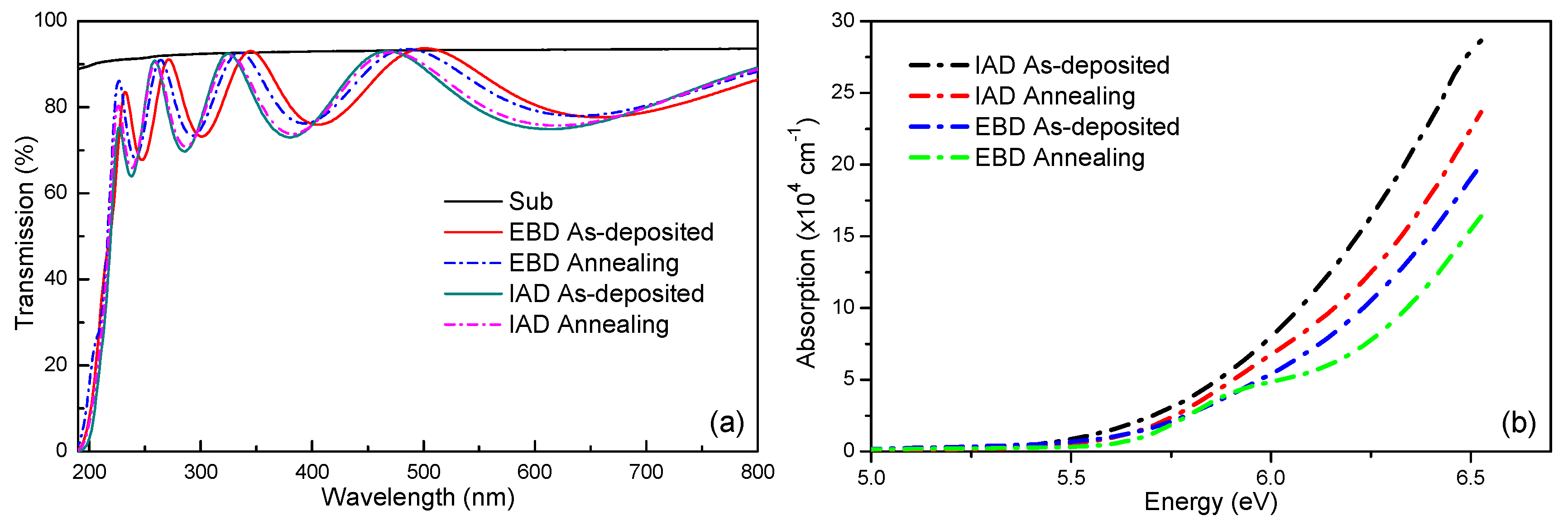
The EBD and IAD HfO2 film samples presented a significantly lower transmission at wavelengths shorter than 250 nm compared to bare fused-silica substrate, as presented in Figure 1a, indicating that the HfO2 films had a strong absorption at the short wavelength range, as presented in Figure 1b. After thermal annealing at 400 °C in air, the transmittance in the short wavelength range improved with decreasing absorption. In the meantime, the refractive index and physical thickness of the films were calculated via a method proposed by Swanepoel [18]. The EBD and IAD films had refractive indices of 1.93 and 2.05 at a wavelength of 400 nm and physical thicknesses of 252 and 227 nm, respectively. After annealing, the refractive indices increased to 1.98 and 2.06, and the thicknesses reduced to 245 and 226 nm, respectively. Unlike the ideal crystal, there were many mesoscopic voids in both the EBD and IAD HfO2 films. Thermal annealing reduced the void density and volume in the film samples, increasing the refractive index and decreasing the physical thickness of the films. The annealing-induced changes in the refractive index and thickness of the IAD film were smaller than that of the EBD film. On the other hand, the weak absorption of the HfO2 films at a wavelength greater than 250 nm was calculated by the method proposed by Swanepoel [18]. The absorption coefficient α of a strong absorption at a wavelength shorter than 250 nm was calculated by the formula [12]:
where T and R are the transmittance and reflectance of the film, respectively, and d is the physical thickness of the film. The relationship between the calculated absorption spectrum presented in Figure 1b shows that the IAD film had a higher absorption than the EBD film. After annealing in air, the absorption of the HfO2 film at a photon energy level higher than 5.5 eV (225 nm) was significantly reduced, which could be related to the reduction of oxygen vacancy defects in the film.
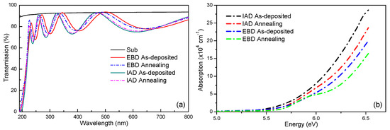
Figure 1.
(a) The transmission of the prepared HfO2 film samples and the substrate; (b) The absorption of the prepared HfO2 film samples. EBD: electron-beam deposition; IAD: ion-assisted deposition; Sub: bare fused-silica substrate.
As HfO2 film is an indirect bandgap material [12,19], the absorption coefficient related to band edge and the photon energy satisfy the following formula:
where hv is the energy of the incident photon, B is the absorption edge width parameter, and Eg is the band gap.
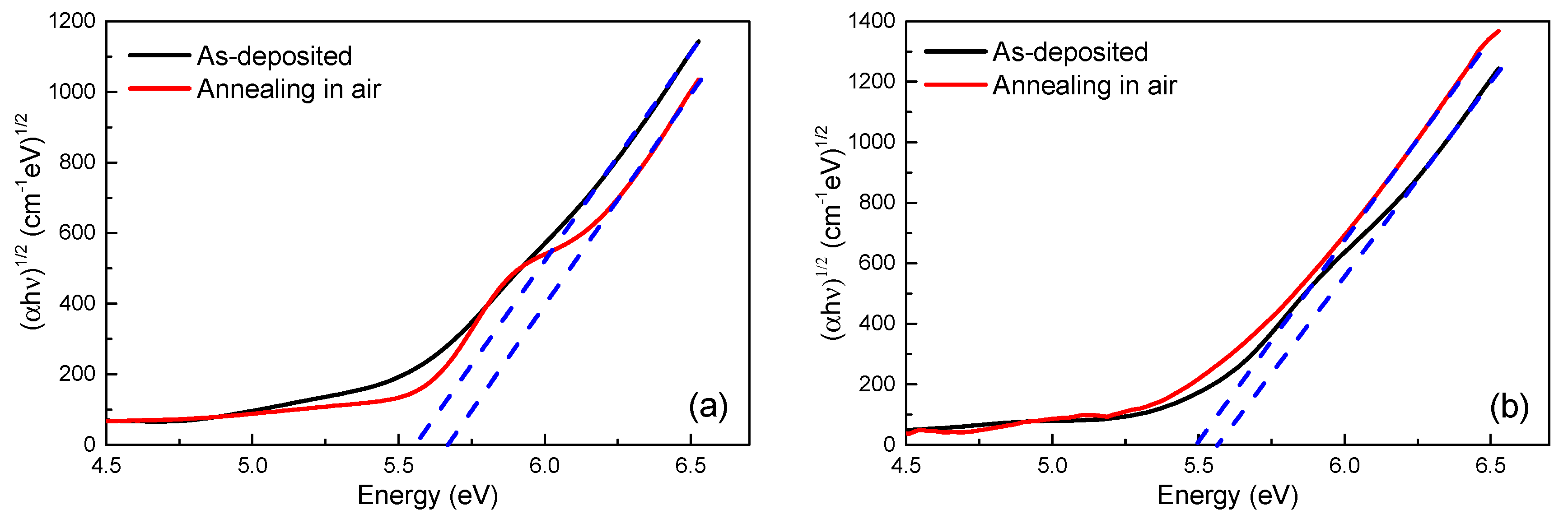
The optical band gap width Eg of the HfO2 film could be determined by the Tauc patterning method, and the results are shown in Figure 2 and Table 1. The bandgap data were consistent with the reported values of 5.25–5.8 eV [14]. The smaller bandgap of the IAD film compared to the EBD film may be related to the increase of the microscopic defects in the film caused by ion bombardment. The absorption spectrum of the EBD film after thermal annealing showed a significant shoulder around 5.8 eV. This shoulder appeared after annealing in air, indicating that it was not caused by oxygen vacancies. Hoppe et al. showed the same results and thought it was intrinsic to monoclinic HfO2 [12], and Aarik et al. indicated it might have originated from excitonic absorption [19].
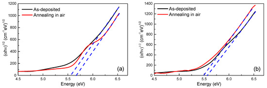
Figure 2.
Tauc patterning calculated from the absorption spectra of (a) EBD and (b) IAD thin films.

Table 1.
The optical bandgap Eg of the HfO2 films.
3.2. Crystalline Structure
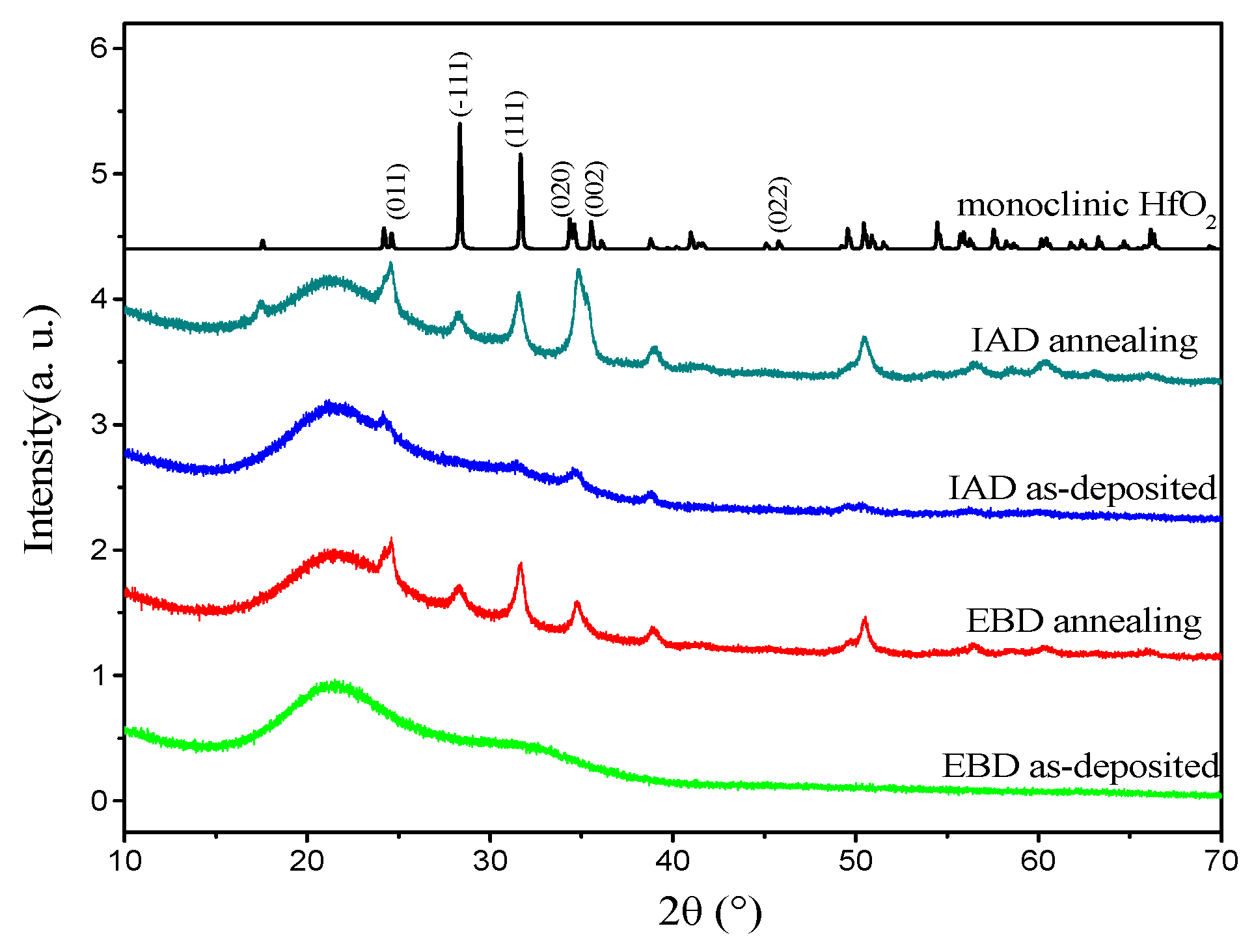
A comparison of the crystalline structures of the HfO2 films before and after thermal annealing (as shown in Figure 3) indicated that the EBD film was amorphous and the monoclinic-phase HfO2 appeared after annealing. The as-deposited IAD film contained a monoclinic phase, and the diffraction peak became stronger after annealing. According to the Scherrer formula, the crystal size D (nm) can be evaluated as:
where K = 0.89 is the Scherrer constant, B is the half-maximum width of the diffraction peak (radians), θ is the diffraction angle, and γ is the X-ray wavelength (0.154056 nm). Defects may have contributed to line broadening and thus caused errors when we used the Scherrer formula. For a rough estimation, we ignored the error and directly used the Scherrer formula to calculate the crystallite sizes of thin films. The crystallite sizes of the EBD and IAD HfO2 films after annealing were 14.90 and 14.40 nm, respectively. The small difference in crystallite size but the significant difference in the absorption shoulder near 5.8 eV after annealing for both the EBD and IAD films, as well as the fact that no absorption shoulder was present for as-deposited and partially crystallized IAD films, clearly indicated that the absorption shoulder was not related to the film crystallization.

Figure 3.
The XRD patterns of the prepared HfO2 films.
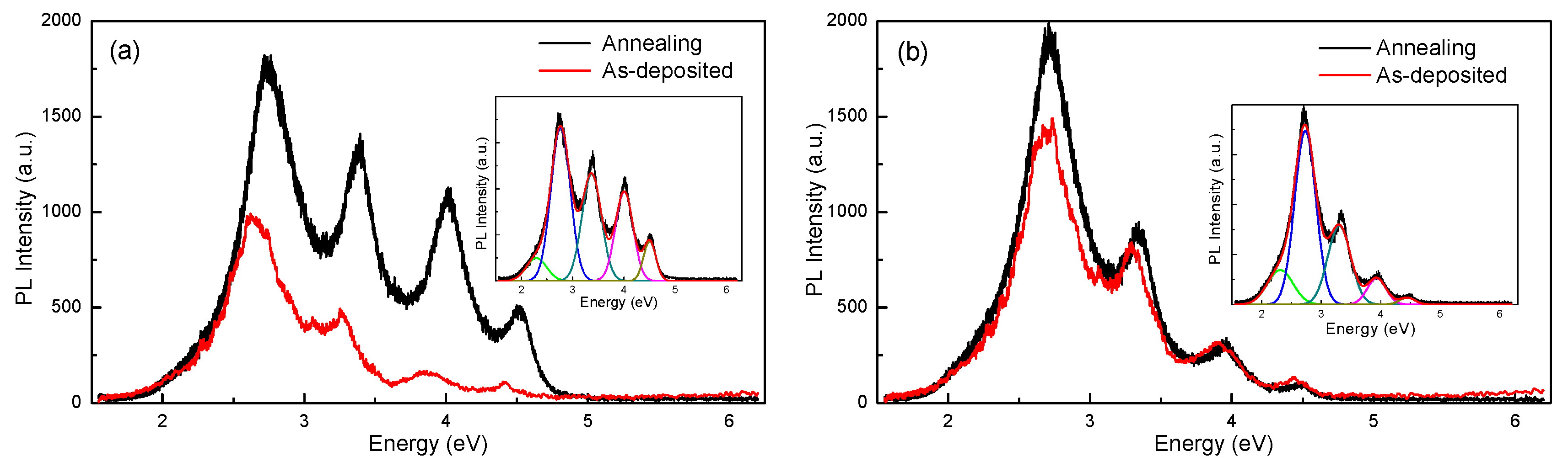
3.3. Photoluminescence
PL is a sensitive and effective tool for the defect characterization of films. In our experiment, a 193 nm (6.4 eV) excimer laser was used as the excitation source for PL measurements. The laser energy density was 2 mJ/cm2. The measured PL spectra of the as-deposited and thermally annealed EBD and IAD HfO2 films are presented in Figure 4. The PL spectra could be decomposed into five PL bands, with corresponding peak positions of approximately 2.3, 2.8, 3.4, 4.0, and 4.4 eV, respectively, as shown in the insets of Figure 4. The PL bands may have originated from self-trapped excitons, radicals, defects, etc. For both the EBD and IAD samples in general, annealing caused increases in peak intensities. The peak intensity increase was much more significant for the EBD film than for the IAD film, which was believed to be related to the annealing-induced crystallization. As the as-deposited IAD film was already partially crystallized, the annealing-induced peak intensity change was relatively small.
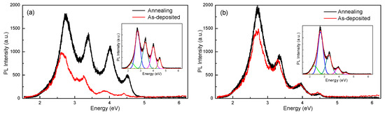
Figure 4.
Photoluminescence (PL) spectra of (a) the EBD HfO2 films and (b) the IAD HfO2 films, excited by 193 nm laser irradiation. The insets are the multi-band fits.
In recent years, PL of HfO2 film has been intensively investigated [13,15,19,20,21,22,23]. Aarik et al. [19] assigned the PL band near 4.4 eV to self-trapped excitons, which caused the absorption shoulder near 5.8 eV. Our absorption and PL measurements confirmed the correlation between the 4.4 eV PL band and the absorption shoulder near 5.8 eV. From Figure 1 and Figure 4, thermal annealing induced the obvious absorption shoulder near 5.8 eV and a significant increase in PL intensity at 4.4 eV for the EBD film, while the influence of annealing on the absorption shoulder near 5.8 and the 4.4 eV PL band of the IAD film was much less significant. For the PL band near 4.0 eV, Rastorguev et al. [20] correlated it to the OH radical in the film. Our experimental results support this assignment. From Figure 1 and Figure 4, thermal annealing induced a smaller change in the refractive index for the IAD film than for the EBD film, which indicated a smaller change in H2O content for the IAD film than for the EBD film, as well as a smaller change in PL intensity near 4.0 eV. On the other hand, the assignments for the 2.3–3.4 eV PL bands of HfO2 film are still disputable: Kiisk et al. [23] and Aarik et al. [19] assigned them to oxygen vacancy defects, while Ito [21] studied HfO2 and ZrO2 with different oxygen contents and concluded that these PL bands were independent of impurities, oxygen vacancies, and interface defects. It was suggested that these PL bands were most likely due to the radiative recombination between localized states at the band tails.
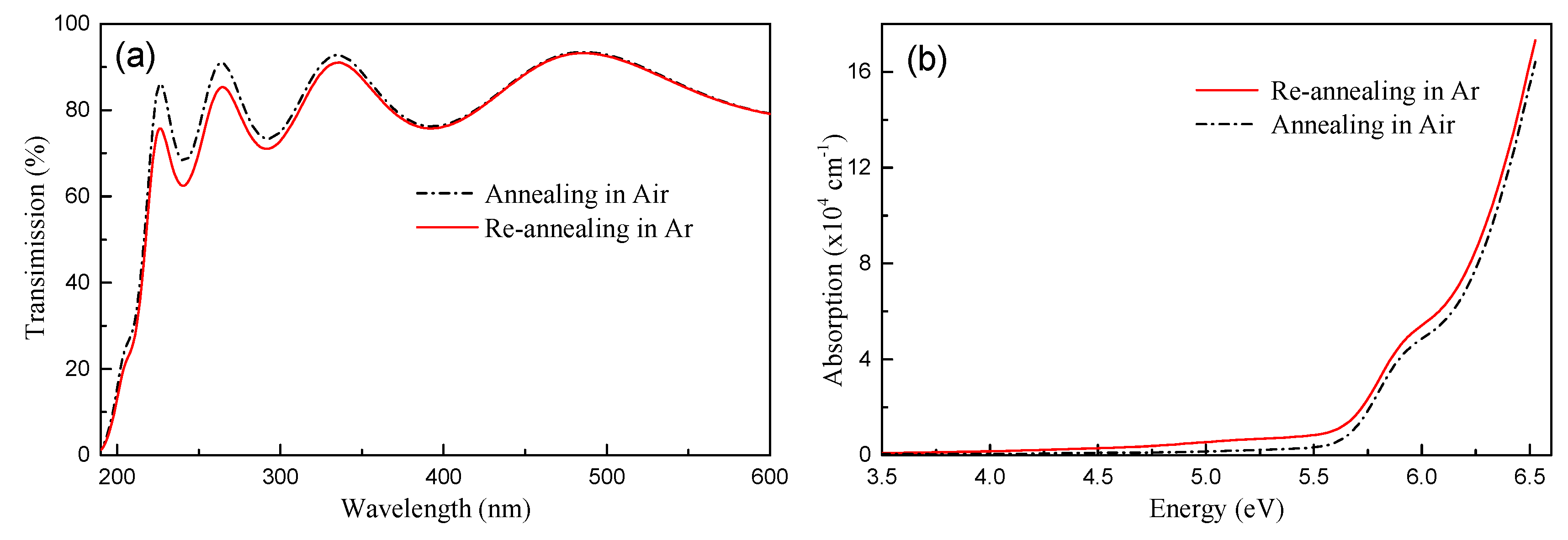
To investigate the correlation between PL and the oxygen vacancy defects in HfO2 films, the sample annealed in air was re-annealed under an Ar gas environment in a tube furnace. The annealing process was the same as in air in order to create only oxygen vacancy defects in the film. After re-annealing in Ar gas, the transmittance of the HfO2 film in the range of 190–400 nm was significantly reduced (Figure 5a). The film absorption (Figure 5b) showed that the oxygen vacancy defects led to an absorption increase over a wide spectral range of 4.0–6.5 eV, and the bandgap of the film was also slightly reduced (Table 1). The changes of the 2.3–3.4 eV PL bands were very small, as presented in Figure 6, indicating that these PL bands were not related to oxygen vacancy defects, in opposition to Kiisk and Aarik’s assumptions [19,23]. Therefore, their assignments need further investigation.
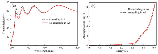
Figure 5.
The (a) transmission and (b) absorption of EBD HfO2 films before and after annealing under Ar gas.
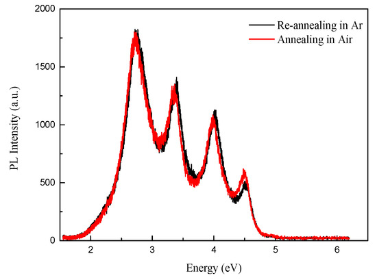
Figure 6.
The PL spectra of the EBD HfO2 film before and after re-annealing in Ar gas, excited by 193 nm laser irradiation.
4. Conclusions
In summary, absorption and photoluminescence measurements were employed to investigate defects in EBD and IAD HfO2 films widely employed in optical coatings and microelectronic devices, which were of great significance for understanding the laser damage mechanism of optical films for high-energy laser applications and the performance improvement of MOS. Experimental results showed that high-temperature thermal annealing in air reduced the absorption of HfO2 films while re-annealing in Ar gas significantly increased the absorption, demonstrating that the absorption loss of the film was closely related to the oxygen vacancy defects. The PL spectra of the HfO2 films showed five bands at approximately 2.3, 2.8, 3.4, 4.0, and 4.4 eV. The experimental results confirmed the assignments of 4.4 and 4.0 eV PL bands to self-trapped excitons and the OH radical, respectively, but refuted the assignments of 2.3–3.4 eV PL bands to oxygen vacancy defects. Further research on correlation between the photoluminescence and localized states of the film is still needed.
Author Contributions
Conceptualization: M.K. and B.L.; Methodology: M.K. and B.L.; Validation: C.G. and P.Z.; Formal Analysis: M.K. and B.L.; Data Curation: W.H. and M.W.; Original Draft Preparation: M.K.; Review and Editing: B.L. and P.Z.
Funding
This research was funded by the National Natural Science Foundation of China, grant number 61805247.
Conflicts of Interest
The authors declare no conflict of interest.
References
- Mazur, M.; Howind, T.; Gibson, D.; Kaczmarek, D.; Morgiel, J.; Wojcieszak, D.; Zhu, W.; Mazur, P. Modification of various properties of HfO2 thin films obtained by changing magnetron sputtering conditions. Surf. Coat. Technol. 2017, 320, 426–431. [Google Scholar] [CrossRef]
- Franke, D.; Hettich, C.; Köhler, T.; Turowski, M.; Ehlers, H.; Ristau, D.; Frauenheim, T. Density functional based tight-binding parametrization of hafnium oxide: Simulations of amorphous structures. Phys. Rev. B 2018, 98, 075207. [Google Scholar] [CrossRef]
- Stenzel, O.; Wilbrandt, S.; Kaiser, N.; Vinnichenko, M.; Munnik, F.; Kolitsch, A.; Chuvilin, A.; Kaiser, U.; Ebert, J.; Jakobs, S.; et al. The correlation between mechanical stress, thermal shift and refractive index in HfO2, Nb2O5, Ta2O5 and SiO2 layers and its relation to the layer porosity. Thin Solid Films 2009, 517, 6058–6068. [Google Scholar] [CrossRef]
- Papernov, S.; Kozlov, A.A.; Oliver, J.B.; Smith, C.; Jensen, L.; Ristau, D.; Gunster, S.; Madebach, H. The role of film interfaces in near-ultraviolet absorption and pulsed-laser damage in ion-beam–sputtered coatings based on HfO2/SiO2 thin-film pairs. Proc. SPIE 2015, 9632, 96320B. [Google Scholar] [CrossRef]
- Wei, Y.; Xu, Q.; Wang, Z.; Liu, Z.; Pan, F.; Zhang, Q.; Wang, J. Growth properties and optical properties for HfO2 thin films deposited by atomic layer deposition. J. Alloy. Compd. 2018, 735, 1422–1426. [Google Scholar] [CrossRef]
- Jena, S.; Tokas, R.B.; Misal, J.S.; Rao, K.D.; Udupa, D.V.; Thakur, S.; Sahoo, N.K. Effect of O2/Ar gas flow ratio on the optical properties and mechanical stress of sputtered HfO2 thin films. Thin Solid Films 2015, 592, 135–142. [Google Scholar] [CrossRef]
- Dijon, J.; Rafin, B.; Pelle, C.; Hue, J.; Ravel, G.; Andre, B. One hundred joule per square centimeter 1.06 um mirrors. Proc. SPIE 2000 3902, 3902, 158–169. [Google Scholar] [CrossRef]
- Kumar, M.; Kumari, N.; Karar, V.; Sharma, A.L. Variable angle spectroscopic ellipsometric characterization of HfO2 thin film. IOP Conf. Ser. Mater. Sci. Eng. 2018, 310, 012132. [Google Scholar] [CrossRef]
- Takeuchi, H.; Ha, D.; King, T.J. Observation of bulk HfO2 defects by spectroscopic ellipsometry. J. Vac. Sci. Technol. A Vac. Surf. Film. 2004, 22, 1337–1341. [Google Scholar] [CrossRef]
- Park, M.H.; Schenk, T.; Hoffmann, M.; Knebel, S.; Gartner, J.; Mikolajick, T.; Schroeder, U. Effect of acceptor doping on phase transitions of HfO2, thin films for energy-related applications. Nano Energy 2017, 36, 381–389. [Google Scholar] [CrossRef]
- Ottking, R.; Kupke, S.; Nadimi, E.; Leitsmann, R.; Lazarevic, F.; Planitz, P.; Roll, G.; Slesazeck, S.; Trentzsch, M.; Mikolajick, T. Defect generation and activation processes in HfO2 thin films: Contributions to stress-induced leakage currents. Phys. Status. Solidi. A 2015, 212, 547–553. [Google Scholar] [CrossRef]
- Hoppe, E.E.; Sorbello, R.S.; Aita, C.R. Near-edge optical absorption behavior of sputter deposited hafnium dioxide. J. Appl. Phys. 2007, 101, 123534. [Google Scholar] [CrossRef]
- Papernov, S.; Brunsman, M.D.; Oliver, J.B.; Hoffman, B.N.; Kozlov, A.A.; Demos, S.G.; Shvydky, A.; Cavalcante, F.H.M.; Yang, L.; Demoni, C.S.; et al. Optical properties of oxygen vacancies in HfO2 thin films studied by absorption and luminescence spectroscopy. Opt. Express 2018, 26, 17608–17623. [Google Scholar] [CrossRef] [PubMed]
- Nguyen, N.V.; Davydov, A.V.; Chandler-Horowitz, D.; Frank, M.M. Sub-bandgap defect states in polycrystalline hafnium oxide and their suppression by admixture of silicon. Appl. Phys. Lett. 2005, 87, 192903. [Google Scholar] [CrossRef]
- Ciapponi, A.; Wagner, F.R.; Palmier, S.; Natoli, J.Y.; Gallais, L. Study of luminescent defects in hafnia thin films made with different deposition techniques. J. Lumin. 2009, 129, 1786–1789. [Google Scholar] [CrossRef]
- Thielsch, R.; Gatto, A.; Heber, J.; Kaiser, N. A comparative study of the UV optical and structural properties of SiO2, Al2O3, and HfO2 single layers deposited by reactive evaporation, ion-assisted deposition and plasma ion-assisted deposition. Thin Solid Films 2002, 410, 86–93. [Google Scholar] [CrossRef]
- Heber, J.; Muhlig, C.; Triebel, W.; Danz, N.; Thielsch, R.; Kaiser, N. Deep UV laser induced luminescence in oxide thin films. Appl. Phys. A 2002, 75, 637–640. [Google Scholar] [CrossRef]
- Swanepoel, R. Determination of the thickness and optical constants of amorphous silicon. J. Phys. E Sci. Instrum. 1983, 16, 1214. [Google Scholar] [CrossRef]
- Aarik, J.; Mändar, H.; Kirm, M.; Pung, L. Optical characterization of HfO2 thin films grown by atomic layer deposition. Thin Solid Films 2004, 466, 41–47. [Google Scholar] [CrossRef]
- Rastorguev, A.A.; Beyi, V.I.; Smirnova, T.P.; Yakovkina, L.V.; Zamoryanskaya, M.V.; Gritsenko, V.A.; Wong, H. Lumminescence of intrinsic and extrinsic defects in hafnium oxide films. Phys. Rev. B 2007, 76, 235315. [Google Scholar] [CrossRef]
- Ito, T.; Maeda, M.; Nakamura, K.; Kato, H.; Ohki, Y. Similarities in photoluminescence in hafnia and zirconia induced by ultraviolet photons. J. Appl. Phys. 2005, 97, 054104. [Google Scholar] [CrossRef]
- Ferrieu, F.; Dabertrand, K.; Lhostis, S.; Ivanova, V.; Martinez, E.; Licitra, C.; Rolland, G. Observation of HfO2 thin films by deep UV spectroscopic ellipsometry. J. Non-Cryst. Solids 2007, 353, 658–662. [Google Scholar] [CrossRef]
- Kiisk, V.; Lange, S.; Utt, K.; Taette, T.; Maendar, H.; Sildos, I. Photoluminescence of sol-gel-prepared hafnia. Phys. B Condens. 2010, 405, 758–762. [Google Scholar] [CrossRef]

© 2019 by the authors. Licensee MDPI, Basel, Switzerland. This article is an open access article distributed under the terms and conditions of the Creative Commons Attribution (CC BY) license (http://creativecommons.org/licenses/by/4.0/).