Abstract
The adsorption and migration of sulphur (S) atoms on the diamond (001) surface were investigated through first principles calculations to discover the inherent law in S-doped diamond film growth. Results indicated that deposited S atoms could abstract the hydrogen atom on the surface. The adsorption energies were in a range of 2.47 to 5.5 eV when S atoms were deposited on the hydrogen terminated surface or the surface with open radical sites (ORSs). The S atom could migrate on the surface of the 3ORS slabs and the energy barrier was approximately 1.35 eV. The calculations of the projected density of states and the analysis of the magnetic moments presented an interesting result, which demonstrated the evolving phenomena in S-doped diamond film growth and discovered the inherent laws. On the 2ORS slabs, the magnetic moment of the S atom became 0.000 μB after bonding with the two carbon atoms. In such case, a new doped C atom combined with the S atom with a triple bond, and then the C–S molecule was desorbed from the surface. The abstraction of the adsorbed S atom results from the fact that S atoms have six electrons in their outermost electron shell. This finding revealed the reason behind the low S incorporation and the growth rate decrease in S-doped diamond film deposition. This discovery also indicated that atoms with six electrons in their outermost electron shell might hardly be doped into the diamond films during the deposition process.
1. Introduction
Sulphur (S)-doped diamond films were studied for many applications, such as n-type semiconductors [1,2,3], electron emission from nano-structured materials [4], field emission for cold cathode devices [5], and hard coatings [6].
S-doped diamond films were studied as shallow-donor dopants for n-type diamond semiconductors. S-shallow donors with activation energy of 0.38 eV were found [7,8] to be connected to boron, which was accidentally added through chemical vapor depositions (CVD) reactor contamination [9]. Calculations on the donor activation energy level of S in diamond presented highly different results, from 0.15 eV [9], over 0.375 eV [10], and to 1.63 eV [11]. S-doped diamond synthesis indicated that S incorporation into diamond films was low. Sternschulte et al. reported that the S incorporation coefficient in boron-free homoepitaxial diamond films was estimated as 10−6 level [12]. Recently, S-doped diamond films were deposited on silicon (Si) substrate [2]. The net sticking probability, the ratio of S in the film to S in the gas phase, was approximately 1 × 10⁻⁴ at 1170 K. Generally, low incorporation rates were not beneficial to n-type semiconductor applications, but were favourable for some optics applications [4]. Many studies of the S-doped diamond film deposition indicated the influence of S doping on film growth and film structure. S doping could lead to the growth rate decrease of diamond films during both hot filaments chemical vapor deposition (HFCVD) and micro plasma chemical vapor deposition (MPCVD) [13,14,15]. Only one research showed that the growth rate of diamond films could slightly increase via S doping at a low deposit temperature (700 °C) [12]. S doping resulted in different morphological changes. Numerous (100) facets or un-facetted Ballas diamond grains were observed in the addition of more than 500 ppm H2S in HFCVD process [13]. In the MPCVD process, increasing H2S input levels from 100 to 1000 ppm significantly increased the proportion of (100) oriented facets; however, increasing H2S levels to 5000 ppm resulted in the rounded appearance of crystal facets [14]. S addition could decrease diamond crystal quality upon the valuation based on the ratio of the height of the diamond peak at 1332 cm−1, Hd, to the height of the graphite band at 1550 cm−1, Hg [14], the sp3 content [3] or the ratio of peak intensities of graphitic phase to diamond (Ig/Idia) in Raman spectroscopy [2]. The above studies on S-doped diamond films showed that film microstructure could be influenced by process parameters. Therefore, the adsorption and migration of S-doped diamond films should be investigated through first-principles calculations.
Zhou el al. studied the equilibrium geometry and the band structure of S-doped diamond using density functional theory (DFT) calculations. Their result indicated that S atoms were spontaneously incorporated into the diamond (100) surface [10]. This result did not agree with experimental results of the other studies [2,12].
The first-principles calculations in our previous studies were conducted to study the doped diamond films and the adsorption and migration of Si, boron (B), yttrium (Y), niobium (Nb), and nitrogen (N) atoms on the diamond (001) surface [16,17,18,19,20,21,22,23]. Results revealed the different features of B, Si, and N dopants in the doped diamond film growth.
Plasma diagnostics [24] and thermodynamic calculations [25] indicated that the C–S species appeared in the plasma region in the S-doped diamond film deposition. However, optical emission spectroscopy showed that S2 was the dominant species [24], and this result agreed well with the observed deposition of S on cool chamber walls [14]. Therefore, the adsorption and migration of S atoms on the diamond (001) surface were investigated in this study.
2. Calculation Methods and Models
In this paper, first-principle calculations were performed by using the Vienna Ab-initio Simulation Package (VASP 5.2) [26,27,28] based on DFT, as previously described [23]. In the calculations, plane wave basis and periodic boundary conditions were utilized to calculate the Kohn–Sham ground state. A projector augmented-wave (PAW) [29,30] was used to calculate the electronic structure. The generalised gradient approximation (GGA), based on the Perdew–Burke–Ernzerhof (PBE) functional [31,32], was employed to describe the local electron density distribution. The k-point sampling of the Brillouin zone was settled by using the Monkhorst–Pack scheme [33] during a self-consistent calculation to identify the electronic ground state. A (5 × 5 × 1) k-point mesh was used for slab calculations. Additionally, spin-polarisation was conducted in all calculations to optimize the structure and configuration. Electron and ion relaxation convergence precisions were 10−4 and 10−3 eV, respectively. The nudged elastic band (NEB) method in VASP [34] was used to calculate the minimum migration energy of atoms on the diamond (001) surface.
Prior to calculating atom migration, a lattice constant of 3.568 Å was determined by adjusting the calculation parameters to optimize the diamond crystalline structure, in which the plane-wave cut-off energy was 350 eV. The calculated lattice constant was close to the experimental value of 3.567 Å [35]. A 4 × 4 × (1 + 8 + 1 + 16) slab, comprising 1 hydrogen layer at the bottom, 8 carbon layers with (4 × 4) carbon atoms per layer, 1 hydrogen layer on the top of carbon layer, and 16 vacuum layers, was used to model the hydrogen-terminated diamond (H-Ter-D) (001) surface, as shown in Figure 1. The height of the vacuum layer was approximately 12.8 Å so that a periodically arranged interference could be prevented. After the relaxation, the diamond (001) surface underwent reconstruction, and a 1.62 Å long dimer bond was formed. Simultaneously, the bond length between the hydrogen atom and the surface carbon atom reached 1.10 Å. The six highly symmetrical positions are shown in Figure 1a,b, which are described in our previous paper [23]. The position P1 was at the bridge site of the dimer ring-closing bond; the position P2 was at the top of the C atom in the carbon dimer; the position P3 was at the bridge site of the dimer ring-opening bond; the position P4 was between the carbon dimer row at the top of the atom in the third layer; the position P5 was between the carbon dimer at the top of the atom in the second layer; and the position P6 was between the carbon dimer at the top of the atom in the second layer. A sulphur atom was relaxed at the six positions to calculate the adsorption energy. The specific definitions of one open radical site (1ORS), 2ORS-R, 2ORS-CO, 2ORS-CC, 3ORS-C, and 3ORS-R slabs shown in Figure 1c are illustrated with relevant textual description.
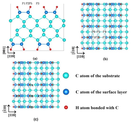
Figure 1.
Symmetrical positions and ORSs on the reconstructed H-Ter-D (001) slab: (a) main view and (b) top view of six highly symmetrical positions and (c) the open radical sites (ORSs) formed by removing different H atoms; when hydrogen B was abstracted, this configuration represents a model of an H-Ter-D (001) with an open radical site, denoted as 1ORS; when hydrogens A and B were abstracted, the configuration represents a model with two ORSs along the dimer row, denoted as 2ORS-R; when hydrogens B and C were abstracted, this configuration represents a model with two ORSs along the dimer chain by the ring-opening side, denoted as 2ORS-CO; when hydrogens E and B were abstracted, the configuration represents a model with two ORSs along the dimer chain by the ring-closing side, denoted as 2ORS-CC; when hydrogens E, B, and C were abstracted, the configuration represents a model with three ORSs along the dimer chain, denoted as 3ORS-C; and when hydrogens A, B, and D were abstracted, this configuration represents a model with three ORSs along the dimer row, denoted as 3ORS-R.
3. Results and Discussion
3.1. On the Fully Hydrogen Terminated Diamond (001) Surface
The adsorption energy Ead of an S atom was computed using Equation (1). Etot is the total configuration energy with an S atom adsorption; Eslab is the energy of the H-Ter-D (001) configuration without the adsorbed atoms, which was −1273.146 eV and Es is the energy of a single S atom. The positive adsorption energy Ead means that the S atom bonds with the surface atoms or adsorbs on the surface. While the negative adsorption energy Ead indicates that the S atom does not bond with the surface atoms or corresponds to an unbinding configuration. By fitting the computed cohesive energy with the experimental results, the energies of a single C atom (Ec) and a single S atom (Es) can be established, Ec is −1.48 eV [36] and Es is −0.91 eV, respectively.
Ead = −(Etot − Eslab − Es)
Figure 2 shows the potential energy surface (PES) of an S atom adsorbed on the fully hydrogen terminated diamond (001) surface. At positions P1 and P3, the adsorption energies were negative, which indicated that the deposited S atom did not bond with the surface C atoms. Moreover, the adsorption energy was small at the position P4, P5, and P6. The distances between the S atom and the surface C atom were between 3.52 and 3.77 Å, which were larger than the covalent radius sum of S and C, 1.79 Å. Therefore, the adsorptions corresponded to physisorptions. At position P2, the S atom abstracted the H atom from the nearest-neighbour carbon (CNN) atom and bonded with the CNN atom. The distance between the S atom and the surface C atom was 1.84 Å. The adsorption energy reached the maximum value of 2.466 eV. As we have reported previously [19,20,23], the C and H atoms were in the chemical saturated state on the H-Ter-D (001) surface. In this case, the deposited atoms were not easily adsorbed on the surface [19,20]. The electronegativity of N was larger than that of carbon; thus, the deposited N atom could abstract the hydrogen atom from the surface carbon atom [23]. The electronegativity of S at 2.58 was almost the same as that of carbon at 2.55, and the S atom would unlikely abstract the H atom from the surface C atom due to its high electronegativity. However, the magnetic moment of the deposited S atom is relatively large at 0.962 μB (Table 1); thus, the activity of the S atom was high, which might cause the S atom to abstract the H atom from the CNN atom.
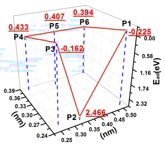
Figure 2.
PES of an S atom adsorbed on the H-Ter-D (001) surface.

Table 1.
Charges and magnetic moments of the atoms of C, H, and S before and after the S atom adsorption.
Figure 3a,b show the charge density difference map of the diamond (001) surface before and after S atom adsorption at the position P2. The red, blue, and green colours display an increase in charge density, a decrease in charge density and a moderate charge density, respectively. The charge density difference map shows that the S atom adsorption caused a significant change in the charge distribution. Bader charge analysis [37,38] and magnetic moment calculations were conducted. Before the S atom adsorbed at P2, the charges of C and H atoms are 3.923 and 0.973 electrons, respectively (Table 1). After the S adsorption, the C atom’s charge amount increases and the S atom’s charge amount decreases. The S atom’s magnetic moment was reduced from 0.962 to 0.000 μB (Table 1), which verified the combination of S atom with CNN and H atoms.
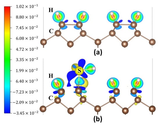
Figure 3.
Charge density difference maps of the diamond (001) surface: (a) H-Ter-D (001) surface and (b) S atom adsorbed at P2 on the surface.
Figure 4 shows the projected density of states (PDOS) of the CNN, H, and S atoms, when the S atom was adsorbed at P2 on the diamond (001) surface. The S 3p orbitals and the CNN 2p orbitals were resonant at −3.5 eV, and the S 3p orbitals and the H 1s orbitals were resonant at −3.65 eV, as exhibited in Figure 4d, demonstrating that the S atom bonded with both the CNN and H atoms.
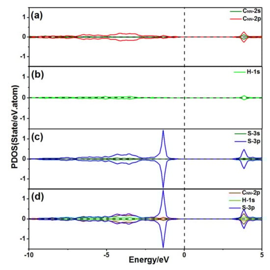
Figure 4.
PDOS of an S atom at P2 adsorbed on the diamond (001) surface: (a) PDOS of the CNN atom; (b) PDOS of the H atom; (c) PDOS of the S atom; and (d) PDOS of the S atom bond with the CNN atom and H atom.
Table 2 presents the adsorption energies of B, Si, N, and S atoms on the fully H-Ter-D (001) surface. The N atom could abstract the H atom and bond with the CNN atom at P2 because of the high electronegativity of N. At P1, the N atom could bond with the two surface C atoms and caused the dimer bond to break. The adsorption energy reached 3.47 eV [23]. The electronegativity of S was almost the same as that of carbon. However, the activity of the deposited S atom was higher than that of the surface CNN atom; thus, the S atom could abstract the H atom and bonded to the CNN atom at P2 with the adsorption energy of 2.466 eV. The electronegativity values of Si and B were lower than that of C, and their adsorption energies on the diamond (001) surface were obviously low.
Table 2.
Adsorption energies Ead (eV) of the atoms of B, Si, N, and S on the H-Ter-D (001) surface.
3.2. On the 1ORS Slab
By removing a hydrogen atom B in Figure 1c, an open radical site (ORS) existed on the surface, denoted as 1ORS. The ORS left a dangling bond for the CNN atom at the corresponding position. The dangling bond played a key role in the introduction of a chemical reaction [19]. The adsorption energy Ead of an S atom was calculated by using Equation (1). The total energy of the configuration of 1ORS slab was −1267.520 eV.
The adsorption energies of an S atom and the distances between the S and CNN atoms (denoted as dS–C) on the 1ORS slab are listed in Table 3. The PES in Figure 5 shows the S adsorption energies on the 1ORS slab. The PES in Figure 5 shows a deep valley shape whose deepest position is at P2. The data in Table 3 indicate that the adsorption energies are proportional to the distances (dS–C) between the S and CNN atoms.
Table 3.
Adsorption energies of the S atom and distances dS–C between the S and CNN atoms on the 1ORS slab.
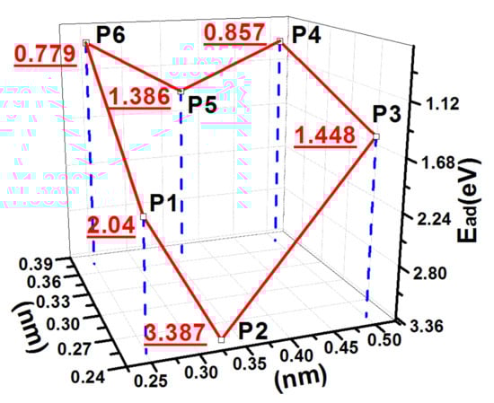
Figure 5.
PES of an S atom on the 1ORS slab.
The data in Table 3 suggest that the smaller the distance between the S atom and the CNN atom, the larger the adsorption energy. Considering that the hydrogen atom B was removed, the S atom deposited at P2 could bond to the surface CNN atoms with the bond length of 1.78 Å, which was close to their covalent radius sum of 1.79 Å. Thus, the adsorption energy reached a maximum value of 3.387 eV.
Figure 6 shows the charge density difference maps of the 1ORS slab and of the S atom at P2, which shows that the S atom bonded with the CNN atom. The charges and magnetic moments of CNN and S atoms before and after S adsorption are listed in Table 4. Only a slight amount of charge transfer was observed before and after the S atom adsorption on the 1ORS slab because the electronegativity of S was close to that of C. The magnetic moment of the CNN atom was 0.364 μB due to the H atom absence before S atom adsorption. After S atom adsorption, the magnetic moment of the CNN atom reduced from 0.364 to 0.014 μB, and the magnetic moment of the S atom decreased from 0.974 to 0.466 μB, verifying the bond between the S and CNN atoms. The magnetic moment of the S atom remained 0.466 μB, indicating that the S atom had unpaired electrons, which were beneficial to the further adsorption of C atoms and C–H radicals.
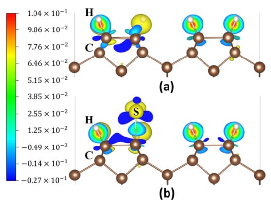
Figure 6.
Charge density difference maps: (a) the 1ORS slab and (b) an S atom adsorbed at P2 on the 1ORS slab.
Table 4.
Charges and magnetic moments of the atoms of CNN and S before and after the S atom adsorption.
The PDOS of the CNN and S atoms on the 1ORS slab are shown in Figure 7a,b. The CNN 2p orbitals and the S 3p orbitals were resonant at −4.5 eV, indicating that the S atom bonded with the CNN atom. Figure 7b shows a clearly asymmetric distribution of S 3p spin-up and down states. This asymmetry is consistent with the magnetic moment of the S atom at 0.466 μB (Table 4).
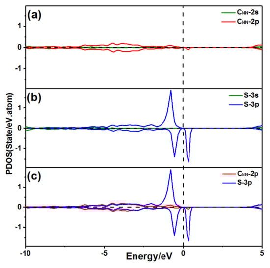
Figure 7.
PDOS of S adsorbed at P2 on the 1ORS slab: (a) PDOS of the CNN atom; (b) PDOS of the S atom; and (c) PDOS of the S atom bond with the CNN atom.
Table 5 shows the adsorption energies of the B, Si, N, and S atoms on the 1ORS slab. The maximum adsorption energy is 5.197 eV corresponding to the B atom adsorbed at P5 [20], 3.068 eV for the Si atom adsorbed at P2 [19], 4.849 eV for the N atom adsorbed at P1 [23], and 3.387 eV for the S atom adsorbed at P2. The maximum adsorption energy of B was larger than that of Si because the B atom at P5 abstracted a hydrogen atom from the nearby surface C atom and bonded with two surface C atoms [20]. The maximum adsorption energy of N was larger than that of Si because the N atom at P1 abstracted the H atom from the surface C atom and bonded with the two surface carbon atoms [23]. The maximum adsorption energy of S was larger than that of Si because the electronegativity of S was larger than that of Si; thus, the C–S bond was stronger than that of Si–C on the 1ORS slab. The above analysis suggested that the presence of open radical sites increased the adsorption energy of each atom.
Table 5.
Adsorption energies Ead (eV) of atoms of B, Si, N, and S on the 1ORS slab.
3.3. On the 2ORS slab
When hydrogen atoms of A and B in Figure 1c were removed, two ORSs alongside the dimer row appeared on the surface, denoted as 2ORS-R. The total energy of the configuration of 2ORS-R slab, Eslab, was −1152.921 eV.
The PES of the adsorption energies of an S atom on the 2ORS-R slab is shown in Figure 8. The adsorption energies of S atoms at P1, P2, P3, and P4 were similar to those of the S atoms adsorbed at the corresponding positions on the 1ORS slab. At P5, because the two hydrogen atoms A and B were removed, the S atom combined with the two CNN atoms with both bond lengths of 1.92 Å. They were slightly longer than their covalent radius sum. In this case, the adsorption energy increased to 4.706 eV.
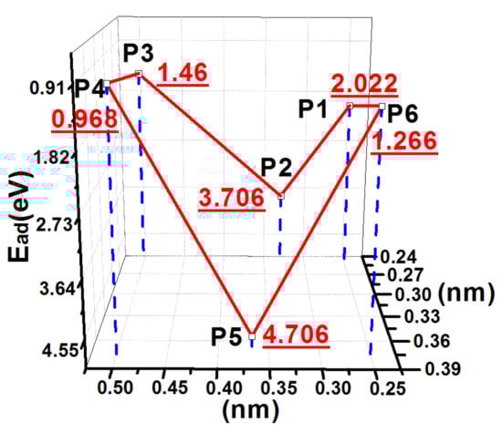
Figure 8.
PES of an S atom on the 2ORS-R slab.
Figure 9 shows the charge density difference map of the 2ORS-R slab. Figure 9b shows the charge density difference map of the 2ORS-R slab with the S atom adsorption at P5, which shows that the S atom has bonded with the two CNN atoms.
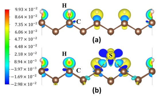
Figure 9.
Charge density difference maps: (a) the 2ORS-R slab and (b) an S atom adsorbed at P5 on the 2ORS-R slab.
The magnetic moments of two CNN atoms were both 0.390 μB before the S atom adsorption, as shown in Table 6, indicating that both CNN atoms had unpaired electrons or dangling bonds. The magnetic moments of two CNN atoms became 0.000 μB after the S atom adsorption, thus verifying that the two CNN atoms bonded with the S atom. Meanwhile, the magnetic moment of the S atom reduced from 0.916 μB to 0.000 μB, indicating that the S atom reached the chemical saturation state, which could influence the adsorption behavior of the following deposited C atoms and the S atom itself. A further analysis will be presented in Section 3.5.
Table 6.
Charges and magnetic moments of the S atom and the CNN atoms before and after S atom adsorption on the 2ORS-R slab.
The spin-up and -down states of the CNN 2p orbitals and the S 3p orbitals (Figure 10) were symmetric for the S adsorption at P5, which agreed well with the fact that the S and two CNN atoms’ magnetic moments all decreased to 0.000 μB. This finding suggested that the S atom and the CNN atoms all reached the saturated construction. The CNN 2p and the S 3p orbitals were resonant at −4.1 eV, implying that the S atom combined with the surface CNN atoms.
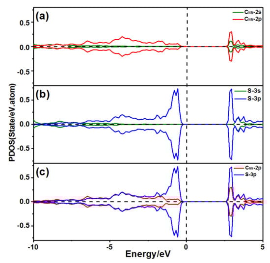
Figure 10.
PDOS of an S atom at P5 adsorbed on the 2ORS-R slab: (a) PDOS of one CNN atom; (b) PDOS of the S atom, and (c) PDOS of the S atom bond with the CNN atoms.
When the hydrogen atoms of B and E were abstracted in Figure 1c, two ORSs alongside the dimer chain by ring-closing side (denoted as 2ORS-CC) appeared on the surface. When the hydrogen atoms of B and C in Figure 1c were removed, two ORSs alongside the dimer chain by ring-opening side (denoted as 2ORS-CO) emerged on the surface. These two configurations were similar to the configuration of 2ORS-R slab. The absence of two hydrogen atoms presented the opportunity for the combination of the deposited S atom and two CNN atoms.
The PES of the 2ORS-CC slab is shown in Figure 11a. The adsorption energies of S atoms at P3, P4, P5, and P6 were similar to those of the S atom adsorption at the corresponding positions on the 1ORS slab. The S atom deposited at P1 bonds to the surface carbon dimer with bond lengths of 1.81 and 1.82 Å, which were close to their covalent radius of 1.79 Å. Thus, the adsorption energy reached a maximum value of 5.50 eV. The PES of the 2ORS-CO slab is shown in Figure 11b. The S atom at P3 bonded to the surface carbon dimer with bond lengths of 1.79 and 1.91 Å, which were close to their covalent radius of 1.79 Å. Thus, the adsorption energy reached 4.859 eV.
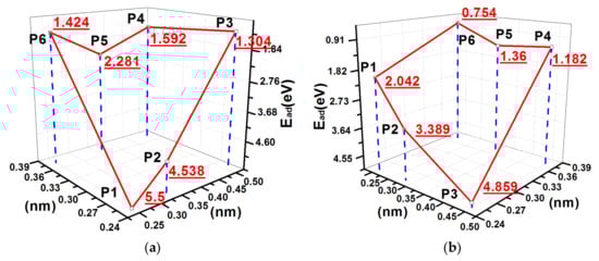
Figure 11.
PES of the S atom adsorption on 2ORS slabs: (a) on the 2ORS-CC slab and (b) on the 2ORS-CO slab.
Figure 12a,b display the charge density difference maps of an S atom at position P1 on the 2ORS-CC slab before and after the S atom adsorption. Figure 12c,d show the charge density difference maps of an S atom at P3 on the 2ORS-CO slab before and after S atom adsorption. Figure 12b,d show that the S atom bonds with the two CNN atoms.
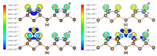
Figure 12.
Charge density difference maps: (a) the 2ORS-CC slab; (b) an S atom adsorbed at P1 on the 2ORS-CC slab; (c) the 2ORS-CO slab; and (d) an S atom adsorbed at P3 on the 2ORS-CO slab.
The magnetic moments of two CNN atoms were 0.251 and 0.167 μB before the S atom was adsorbed on the 2ORS-CC slab, as shown in Table 7, indicating that the two CNN atoms had unpaired electrons. After the S atom adsorption, the magnetic moments of the two CNN atoms became 0.000 μB, thus indicating that the two CNN atoms bonded with the S atom. In this adsorption process, the magnetic moment of the S atom decreased from 0.965 to 0.000 μB, indicating that the S atom bonded with the two CNN atoms and was in the chemical saturation state.
Table 7.
Charges and magnetic moments of CNN atoms and S atom before and after the S atom adsorption on the 2ORS-CC and 2ORS-CO slabs.
The spin-up and -down states of the CNN 2p orbitals and the S 3p orbitals were symmetric when an S atom adsorbed at position P1 on the 2ORS-CC slab, shown in Figure 13a,b, which agreed well with the fact that the S atom and two CNN atoms’ magnetic moments were 0.000 μB. As shown in Figure 13c, the CNN 2p orbitals and the S 3p orbitals were resonant at −3.15 eV, indicating the bonding between these atoms. Figure 13d–f shows the PDOS of the S atom adsorption on the 2ORS-CO slab, which is similar to the case of the S atom adsorption on the 2ORS-CC slab.
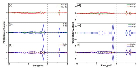
Figure 13.
PDOS of the S atom adsorption on the diamond (001) surface: (a) PDOS of the CNN atom with 2ORS-CC slab; (b) PDOS of the S atom with 2ORS-CC slab; (c) PDOS of the S atom bonded to the CNN atom with 2ORS-CC slab; (d) PDOS of the CNN atom with 2ORS-CO slab; (e) PDOS of the S atom with 2ORS-CO slab; and (f) PDOS of the S atom bonded to the CNN atom with 2ORS-CO slab.
In summary, the S atom can adsorb stably on the 2ORS slabs with relatively large adsorption energies from 4.7 to 5.5 eV. The charge density difference maps, the magnetic moment changes and the PDOS results revealed the bonding between the deposited S atom and the surface CNN atoms. Remarkably, after bonding with the two surface CNN atoms, the magnetic moment of the S atom became 0.000 μB, which could influence the adsorption of the subsequent C atoms and the S atom itself.
3.4. On the 3ORS Slab
When the hydrogen atoms E, B, and C in Figure 1c were abstracted, three open radical sites appeared along the dimer chain, which was denoted as 3ORS-C. When the hydrogen atoms of A, B, and D in Figure 1c were removed, three open radical sites emerged along the dimer row, which was denoted as 3ORS-R.
The configuration of the removed hydrogen atoms E, B, and C were equivalent to the configurations of 2ORS-CC and 2ORS-CO. The PES of adsorption energy of the S atom on the 3ORS-C slab is shown in Figure 14a, and two deep valleys are found on the PES. One deep point was at the position P3 and the other was at the position P1. Therefore, the migration path for the S atom on the direction of dimer chain was from the position P3 to the position P1.
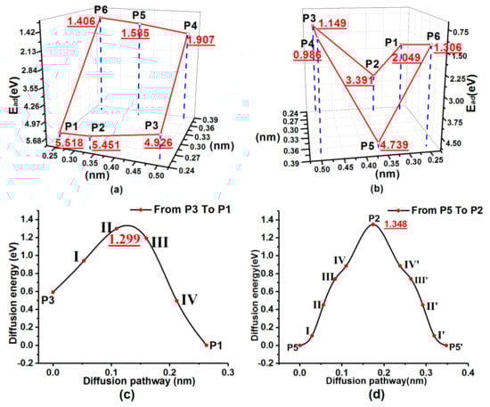
Figure 14.
PES and minimum migration energy path curves of 3ORS slabs: (a) PES of an S atom on the 3ORS-C slab; (b) PES of an S atom on the 3ORS-R slab; (c) minimum migration energy path curves for the S atom migration on the 3ORS-C slab from P3 to P1; and (d) minimum migration energy path curves for the S atom migration on the 3ORS-R slab from P5 through P2 to P5′.
Similarly, the configuration of the removed hydrogen atoms A, B and D were equivalent to the configuration of the two connected 2ORS-R. The PES of adsorption energy of the S atom on the 3ORS-R slab is displayed in Figure 14b. There were two deep valleys on the PES. One deep point was at the position P5 [between A and B in Figure 1c] and the other deep point was at the position P5′ [between B and D in Figure 1c]. The two deep valleys on the PES are symmetric to the position P2. The one valley by the position P5 side is displayed in Figure 14b. The migration path of the S atom was from the position P5 through the saddle point P2 to the position P5′.
Table 8 presents the calculation data of the minimum migration energies, and Figure 14c,d show the fitting curves. In the case of 3ORS-C, Figure 14c and Table 8 show that the energy barrier required for the S atom to migrate from P1 to P3 is 1.299 eV.
Table 8.
Minimum migration energies of an S atom on the 3ORS slabs.
Similarly, in the case of 3ORS-R, the energy barrier for the S atom to migrate from P5 through P2 to P5’ is 1.348 eV (Figure 14d and Table 8).
In summary, S atoms can be stably adsorbed on the diamond (001) surface with three open radical sites. On the 3ORS-C and 3ORS-R slabs, the minimum migration activation energies of S atoms were 1.299 and 1.348 eV, respectively.
3.5. Adsorption of a C Atom Deposited to the Region Near the S Atom Adsorbed on the 2ORS-R Slab
The magnetic moment of the S atom was 0.000 μB when an S atom bonded with the two surface CNN atoms on the 2ORS-R slab, which reflected the intrinsic quality of S atoms. The S atom has six electrons in its outermost electron shell. Upon combining of the S atom with the two surface CNN atoms, S had eight electrons in its valence shell. According to the octet rule, the magnetic moment of S should be 0.000 μB. In this case, a C atom with four unpaired electrons deposited close to the S atom, which naturally influenced the adsorption of the S atom. To study this effect, the adsorption behavior of the C atom deposited to the region near the S atom that adsorbed on the 2ORS-R slab was investigated.
After the newly introduced carbon atom (CNEW) stably bonded with the S atom, the distance between the S atom and the surface CNN atom increased from 1.92 to 2.33 Å, which was larger than their covalent radius sum of 1.79 Å. Thus, the bonding between the S atom and the surface CNN atom was loose and tended to break. Meanwhile, the distance between the S atom and the CNEW atom was 1.55 Å, which was smaller than their covalent bond radius sum of 1.79 Å; thus, the two atoms were combined to form a C–S molecule.
Figure 15a,b show the charge density difference maps of the S atom on the 2ORS-R slab before and after the CNEW atom adsorption. Before the CNEW atom adsorption, the S atom stably bonded with two surface CNN atoms. After the CNEW atom adsorption, the S atom bonded with the CNEW atom and tended to be desorbed from the diamond (001) surface. A large number of electrons gathered around the CNEW atom, as shown in blue and green in Figure 15b.
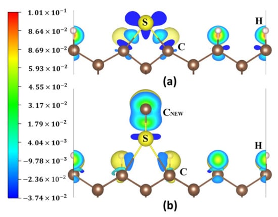
Figure 15.
Charge density difference maps: (a) S atom adsorbed at P5 on the 2ORS-R slab; (b) CNEW atom adsorbed at P5 on the 2ORS-R slab with an S atom.
Table 9 lists the charge amount and magnetic moments of CNN, CNEW and S atoms before and after the CNEW atom adsorption. After the CNEW atom adsorption, the charge amounts of the S atom reduced from 6.048 to 5.540 electrons, whereas those of the CNEW atom increased from 4.096 to 4.628 electrons. This finding quantitatively showed the acquired electron effect of the CNEW atom, as displayed in Figure 15b. The charge amounts of the CNN1 and CNN2 atoms were slightly increased. The magnetic moment of the CNEW atom was 1.023 μB before the CNEW atom adsorption, thus manifesting the strong chemical activity of the CNEW atom. After the CNEW atom adsorption, the magnetic moment of S, CNEW, CNN1, and CNN2 atoms is 0.000 μB, indicating that the four atoms were in chemically stable states.
Table 9.
Charge and magnetic moments of CNN, CNEW, and the S atoms before and after the CNEW atom adsorption.
Figure 16a–c show the PDOS of the atoms of CNN, CNEW and S, respectively. Figure 16d shows the PDOS of the CNEW 2s orbitals, CNEW 2p orbitals, S 3s orbitals, S 3p orbitals, and CNN 2p orbitals.
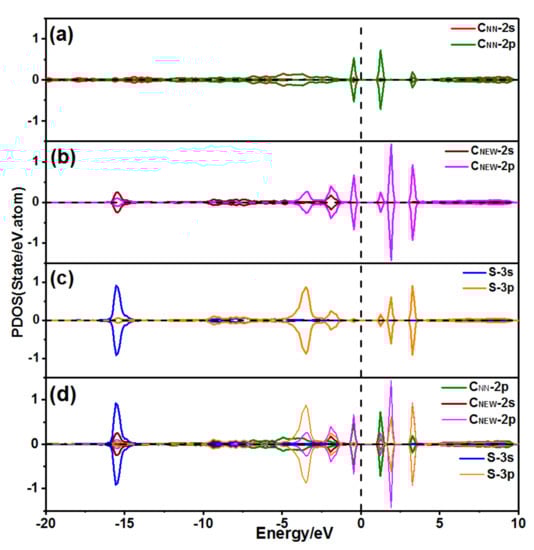
Figure 16.
PDOS of a 1S1C atom adsorbed on the 2ORS-R slab: (a) PDOS of the CNN atom; (b) PDOS of the CNEW atom; (c) PDOS of the S atom; and (d) PDOS of the CNN atom bond with the S and CNEW atoms.
The CNEW 2s orbitals and the S 3s orbitals were resonant at −15 eV, as shown in Figure 16 b–d, meanwhile, the CNEW 2p orbitals and the S 3p orbitals were resonant at −3.15 and −1.8 eV so that the atoms of CNEW and S were combined with a C–S triple bond.
The CNEW 2p orbitals and the CNN 2p orbitals were resonant at −0.45 eV, as shown in Figure 16a,b,d), which indicated that the CNEW atom bonded with two CNN atoms. The magnetic moments of CNN1 and CNN2 atoms were 0.000 μB, which implied the bonding between the surface CNN atoms and the CNEW–S molecule. The bonding of the surface CNN atoms and the CNEW–S molecule was at −0.45eV, being close to the Fermi line. Therefore, the bonding might easily break.
Two additional calculations were conducted. The first one, a new hydrogen atom deposited to one surface CNN atom when the CNEW–S molecule combined with it. The calculation results showed that the distance between the S atom and the CNN atom increased from 2.33 to 3.98 Å, indicating the bonding between the CNEW–S molecule and the surface CNN atoms was loose. Meanwhile, the distance between the H atom and the CNN atom was 1.10 Å, thus manifesting the combination of the new H atom with the CNN atom. Additionally, the bond length of the CNEW–S molecule was 1.54 Å, demonstrating the CNEW–S molecule was stable. The second one, two new hydrogen atoms deposited to two surface CNN atoms when the CNEW–S molecule combined with them. The results showed that the distance between the S atom and the CNN atom further increased to 4.25 Å, indicating the CNEW–S molecule to be desorbed from the surface. Meanwhile, the distance between the H atom and the CNN atom was 1.10 Å and the bond length of the CNEW–S molecule was 1.54 Å. Therefore, the molecule CNEW-S was easily desorbed from the diamond (001) surface.
Plasma diagnostics [24] indicated that the C–S species were in the plasma region. These C–S species might come from the desorption of the C–S molecule, which led to the low S incorporation rate of the S-doped diamond films.
In summary, the S atoms that stably adsorbed on the 2ORS-R slab could be abstracted by a deposited CNEW atom and hence formed a C–S molecule with a C–S triple bond. The two surface CNN atoms could bond with the C–S molecule. Therefore, the four atoms all were in chemically stable state. However, the chemical bonds between the C–S molecule and the two surface CNN atoms were relatively weak, so they easily broke. Therefore, the C–S molecule tended to be desorbed from the diamond (001) surface. From this point of view, the S atom deposited on the diamond (001) surface firstly underwent a stable adsorption and then desorption from the diamond (001) surface in the form of a C–S molecule. This phenomenon indicated that the S atoms were difficult to incorporate into the diamond films. In other words, the direct S doping method can intrinsically fabricate the S-doped diamond films with low S incorporation rate. Some experimental results demonstrated the low S incorporation rate in the S-doped diamond films [2,12]. If the high S incorporation rate into the diamond films is important, the other composition method should be determined.
4. Conclusions
In the above study, first-principles calculations were carried out to reveal the inherent law in the S-doped diamond film growth. The calculations focused on the adsorption and migration of an S atom on the hydrogen terminated diamond (001) surface without and with open radical sites (ORSs). Results presented the following conclusions:
- According to the calculation results, deposited S atoms can be adsorbed on diamond (001) surface. When the surface was fully hydrogen terminated, a deposited S atom can abstract a hydrogen atom and then was adsorbed there with adsorption energy of 2.47 eV. When one or two ORSs existed on the surface, the adsorption energy increased to 3.39 or 5.5 eV.
- The S atom can migrate on the 3ORS slabs and the energy barrier was approximately 1.35 eV. This means that S atoms may easily diffuse at the deposition temperature over 1000 K in accordance with the Arrhenius equation [39].
- An interesting evolving phenomenon was demonstrated through the PDOS calculations and the magnetic moment analysis and the inherent law was discovered. On the 2ORS slabs, the magnetic moment of the S atom became 0.000 μB after combining with the two surface C atoms. In such case, a new deposited C atom will combine with the S atom with a triple bond, and then the C–S molecule will be desorbed from the surface. The abstraction of the adsorbed S atom results from the fact that S atoms have six electrons in their outermost electron shell. This finding revealed the reason behind the low S incorporation and the growth rate decrease in S-doped diamond film deposition. This discovery also indicated that atoms with six electrons in their outermost electron shell might hardly be doped into the diamond films during the CVD process.
Author Contributions
Conceptualization, X.L.; Methodology, X.L., Y.R. and S.S.; Formal Analysis, H.S.; Investigation, H.S. and Y.W.; Writing–Original Draft Preparation, X.L. and H.S.; Writing–Review and Editing, X.L. and H.S.; Supervision, X.T. and H.J.; Project Administration, X.L.; Funding Acquisition, X.L.
Funding
This research was funded by the National Natural Science Foundation of China (Nos. 50845065, 51562031, and 61765012), the Natural Science Foundation of Inner Mongolia Autonomous Region (Nos. 2014MS0516 and 2015MS0550) and the Science and Technology Committee of Baotou City (No 2013J2001-1) for supporting this study.
Conflicts of Interest
The authors declare no conflict of interest. The sponsors played no role in study design; collection, analysis, and interpretation of data; writing of the report. All authors make the decision to submit the report for publication. The sponsors had no such involvement in the decision of submission.
References
- Goss, J.P.; Eyre, R.J.; Briddon, P.R. Theoretical models for doping diamond for semiconductor applications. Phys. Status Solidi B 2008, 245, 1679–1700. [Google Scholar] [CrossRef]
- Nose, K.; Suwa, T.; Fujita, R.; Kamiko, M.; Mitsuda, Y. Crystallinity and electrical conductivity of sulphur-containing microcrystalline diamond thin film. Thin Solid Films 2012, 520, 4310–4313. [Google Scholar] [CrossRef]
- Wang, Y.; Yin, Z. Structural and electrical properties of Sulphur-doped diamond thin films. Plasma Sci. Technol. 2014, 16, 255–259. [Google Scholar] [CrossRef]
- Koeck, F.A.M.; Zumer, M.; Nemanic, V.; Nemanich, R.J. Photo and field electron emission microscopy, from sulphur doped nanocrystalline diamond films. Diam. Relat. Mater. 2006, 15, 880–883. [Google Scholar] [CrossRef]
- Morell, G.; González-Berríos, A.; Weiner, B.R.; Gupta, S. Synthesis, structure, and field emission properties of sulphur-doped nanocrystalline diamond. J. Mater. Sci. Mater. Electron. 2006, 17, 443–451. [Google Scholar] [CrossRef]
- Haubner, R.; Ullram, S. Influence of H2S addition during diamond deposition on hard metal substrates. Diam. Relat. Mater. 2008, 17, 1100–1105. [Google Scholar] [CrossRef]
- Sakaguchi, I.; Gamo, M.N.; Kikuchi, Y.; Yasu, E.; Haneda, H. Sulphur: A donor dopant for n-type diamond semiconductors. Phys. Rev. B 1999, 60, R2139–R2141. [Google Scholar] [CrossRef]
- Nishitani-Gamo, M.; Yasu, E.; Xiao, C.; Kikuchi, Y.; Ushizawa, K.; Sakaguchi, I.; Suzuki, T.; Ando, T. Sulphur-doped homoepitaxial (001) diamond with n-type semiconductive properties. Diam. Relat. Mater. 2000, 9, 941–947. [Google Scholar] [CrossRef]
- Saada, D.; Adler, J.; Kalish, R. Sulfur: A potential donor in diamond. Appl. Phys. Lett. 2000, 77, 878–879. [Google Scholar]
- Zhou, H.; Yokoi, Y.; Tamura, H.; Takami, S.; Kubo, M.; Miyamoto, A.; Mikka, N.; Ando, T. Quantum chemical calculations of Sulphur doping reactions in diamond CVD. Jpn. J. Appl. Phys. 2001, 40, 2830–2832. [Google Scholar] [CrossRef]
- Katayama-Yoshida, H.; Nishimatsu, T.; Yamamoto, T.; Orita, N. Codoping method for the fabrication of low-resistivity wide band-gap semiconductors in p-type GaN, p-type AlN and n-type diamond: Prediction versus experiment. J. Phys. Condens. Matter 2001, 13, 8901–8914. [Google Scholar] [CrossRef]
- Sternschulte, H.; Schreck, M.; Stritzker, B.; Bergmaier, A.; Dollinger, G. Growth and properties of CVD diamond films grown under H2S addition. Diam. Relat. Mater. 2003, 12, 318–323. [Google Scholar] [CrossRef]
- Haubner, R.; Sommer, D. Hot-filament diamond deposition with Sulphur addition. Diam. Relat. Mater. 2003, 12, 298–305. [Google Scholar] [CrossRef]
- Petherbridge, J.R.; May, P.W.; Fuge, G.M. Sulphur doping of diamond films: Spectroscopic, electronic, and gas-phase studies. J. Appl. Phys. 2002, 91, 3605–3613. [Google Scholar] [CrossRef]
- Nishitani-Gamo, M.; Xiao, C.Y.; Zhang, Y.F.; Yasu, E.; Kikuchi, Y.; Sakaguchi, I.; Suzuki, T.; Sato, Y.; Ando, T. Homoepitaxial diamond growth with Sulphur-doping by microwave plasma-assisted chemical vapour deposition. Thin Solid Films 2001, 382, 113–123. [Google Scholar] [CrossRef]
- Liu, X.; Yin, Y.J.; Ren, Y.; Wei, H. Adsorption and evolution behaviour of 4C1Si island configurations on diamond (001) surface: A first principle study. J. Alloy. Compd. 2015, 618, 516–521. [Google Scholar] [CrossRef]
- Liu, X.; Luo, H.; Ren, Y.; Xia, Q.; Li, W.; Tan, X.; Sun, S. Theoretical study of the migration behaviour of Y–C atoms on diamond (001) surface. Diam. Relat. Mater. 2016, 61, 102–108. [Google Scholar] [CrossRef]
- Liu, X.; Li, W.; Ren, Y.; Luo, H.; Xia, Q.; Tan, X.; Sun, S. Adsorption and migration behaviours of Nb–C atoms on clean diamond (001) surface: A first principles study. Comput. Mater. Sci. 2016, 121, 159–166. [Google Scholar] [CrossRef]
- Liu, X.; Qiao, H.; Kang, C.; Ren, Y.; Tan, X.; Sun, S. Adsorption and migration behaviour of Si atoms on the hydrogen-terminated diamond (001) surface: A first principles study. Appl. Surf. Sci. 2017, 420, 542–549. [Google Scholar] [CrossRef]
- Liu, X.; Kang, C.; Qiao, H.; Ren, Y.; Tan, X.; Sun, S. Theoretical studies of the adsorption and migration behaviour of boron atoms on hydrogen-terminated diamond (001) surface. Coatings 2017, 7, 57. [Google Scholar]
- Liu, X.; Lu, P.; Wang, H.; Ren, Y.; Tan, X.; Sun, S.; Jia, H. Morphology and structure of Ti-doped diamond films prepared by microwave plasma chemical vapour deposition. Appl. Surf. Sci. 2018, 442, 529–536. [Google Scholar] [CrossRef]
- Liu, X.; Wang, H.; Lu, P.; Ren, Y.; Tan, X.; Sun, S.; Jia, H. Effect of the N/C ratios of ammonia added to process gas mixtures on the morphology and structure of MPCVD diamond films. Coatings 2018, 8, 163. [Google Scholar] [CrossRef]
- Liu, X.; Wang, H.; Lu, P.; Ren, Y.; Tan, X.; Sun, S.; Jia, H. First principles calculations of the adsorption and migration behaviours of nitrogen atoms on the H-terminated diamond (001) surface. Appl. Surf. Sci. 2019, 463, 668–678. [Google Scholar] [CrossRef]
- Petherbridge, J.R.; May, P.W.; Fuge, G.M.; Rosser, K.N.; Ashfold, M.N.R. In situ plasma diagnostics of the chemistry behind sulphur doping of CVD diamond films. Diam. Relat. Mater. 2002, 11, 301–306. [Google Scholar] [CrossRef]
- Haubner, R. Diamond deposition with sulphur addition—Thermodynamic calculations. Diam. Relat. Mater. 2004, 13, 648–655. [Google Scholar] [CrossRef]
- Kresse, H. Ab initio molecular dynamics for liquid metals. Phys. Rev. B Condens. Matter 1993, 48, 13115–13118. [Google Scholar] [CrossRef]
- Kresse, G. Efficient iterative schemes for ab initio total-energy calculations using a plane-wave basis set. Phys. Rev. B Condens. Matter 1996, 54, 11169–11186. [Google Scholar] [CrossRef]
- Kresse, G.; Furthmüller, J. Efficiency of ab-initio total energy calculations for metals and semiconductors using a plane-wave basis set. Comput. Mater. Sci. 1996, 6, 15–50. [Google Scholar] [CrossRef]
- Blöchl, P.E. Projector augmented-wave method. Phys. Rev. B Condens. Matter 1994, 50, 17953–17979. [Google Scholar] [CrossRef]
- Kresse, G.J.; Joubert, D.P. From ultrasoft pseudopotentials to the projector augmented-wave method. Phys. Rev. B 1999, 59, 1758–1775. [Google Scholar] [CrossRef]
- Perdew, J.P.; Burke, K.; Ernzerhof, M. Generalized gradient approximation made simple. Phys. Rev. Lett. 1996, 77, 3865–3868. [Google Scholar] [CrossRef]
- Perdew, J.P.; Ruzsinszky, A.; Csonka, G.I.; Vydrov, O.A.; Scuseria, G.E.; Constantin, L.A.; Zhou, X.; Burke, K. Restoring the density-gradient expansion for exchange in solids and surfaces. Phys. Rev. Lett. 2008, 100, 136406. [Google Scholar] [CrossRef]
- Monkhorst, H.J.; Pack, J.D. Special points for Brillouin-zone integrations. Phys. Rev. B Condens. Matter 1977, 16, 5188–5192. [Google Scholar] [CrossRef]
- Henkelman, G.; Jóhannesson, G.; Jónsson, H. Methods for finding saddle points and minimum energy paths. In Theoretical Methods in Condensed Phase Chemistry; Springer: Dordrecht, The Netherland, 2002; pp. 269–302. [Google Scholar]
- Kittel, C. Introduction to Solid State Physics, 8th ed.; JohnWiley & Sons Inc.: New York, NY, USA, 2005; p. 59. [Google Scholar]
- Liu, X.J.; Zhang, S.H.; Jiang, Y.J.; Ren, Y. Interface structure of nanodiamond composite films: First-principles studies. J. Alloy. Compd. 2014, 599, 183–187. [Google Scholar] [CrossRef]
- Henkelman, G.; Arnaldsson, A.; Jónsson, H. A fast and robust algorithm for Bader decomposition of charge density. Comput. Mater. Sci. 2006, 36, 254–360. [Google Scholar] [CrossRef]
- Tang, W.; Sanville, E.; Henkelman, G. A grid-based Bader analysis algorithm without lattice bias. J. Phys. Condens. Matter 2009, 21, 084204. [Google Scholar] [CrossRef]
- Butler, J.E.; Mankelevich, Y.A.; Cheesman, A.; Ma, J.; Ashfold, M.N.R. Understanding the chemical vapour deposition of diamond: Recent progress. J. Phys. Condens. Matter 2009, 21, 364201. [Google Scholar] [CrossRef]
© 2019 by the authors. Licensee MDPI, Basel, Switzerland. This article is an open access article distributed under the terms and conditions of the Creative Commons Attribution (CC BY) license (http://creativecommons.org/licenses/by/4.0/).