Effects of Yttrium Doping on a-IGZO Thin Films for Use as a Channel Layer in Thin-Film Transistors

Abstract
:1. Introduction
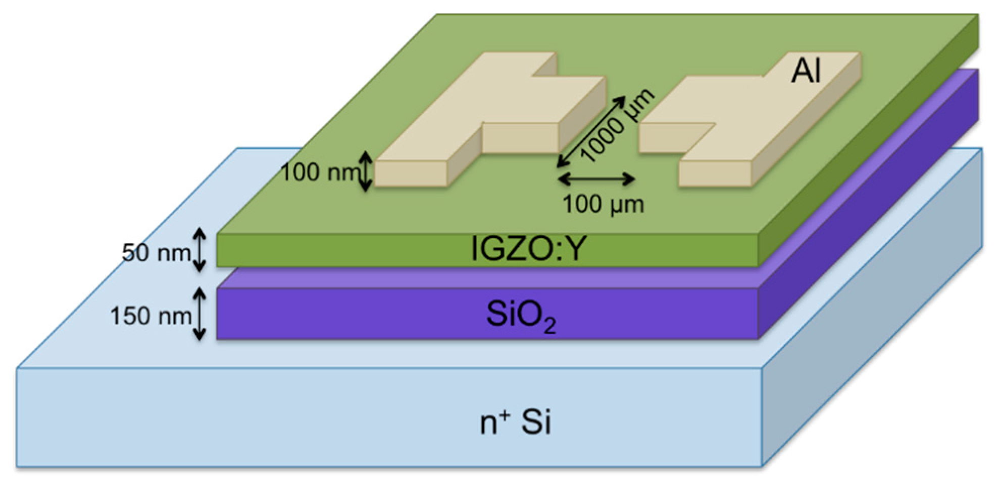
2. Experimental Details
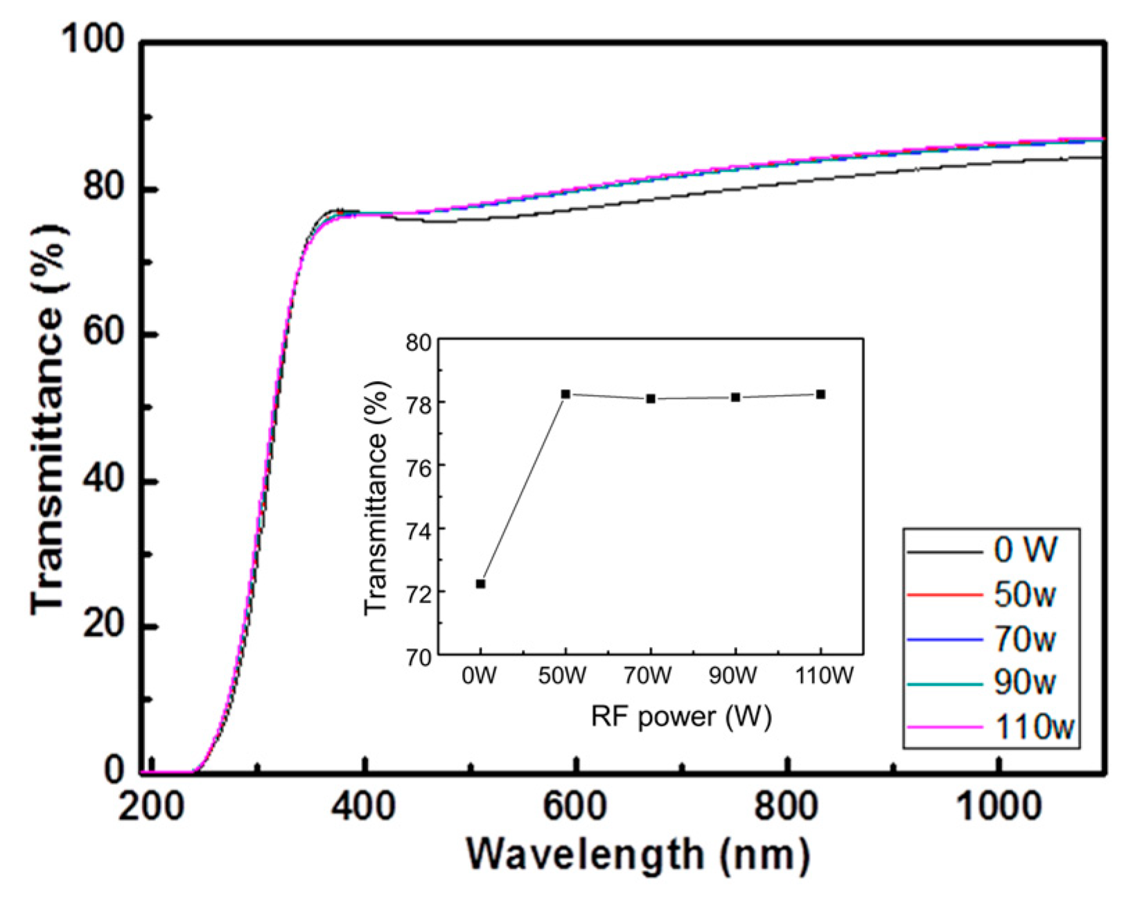
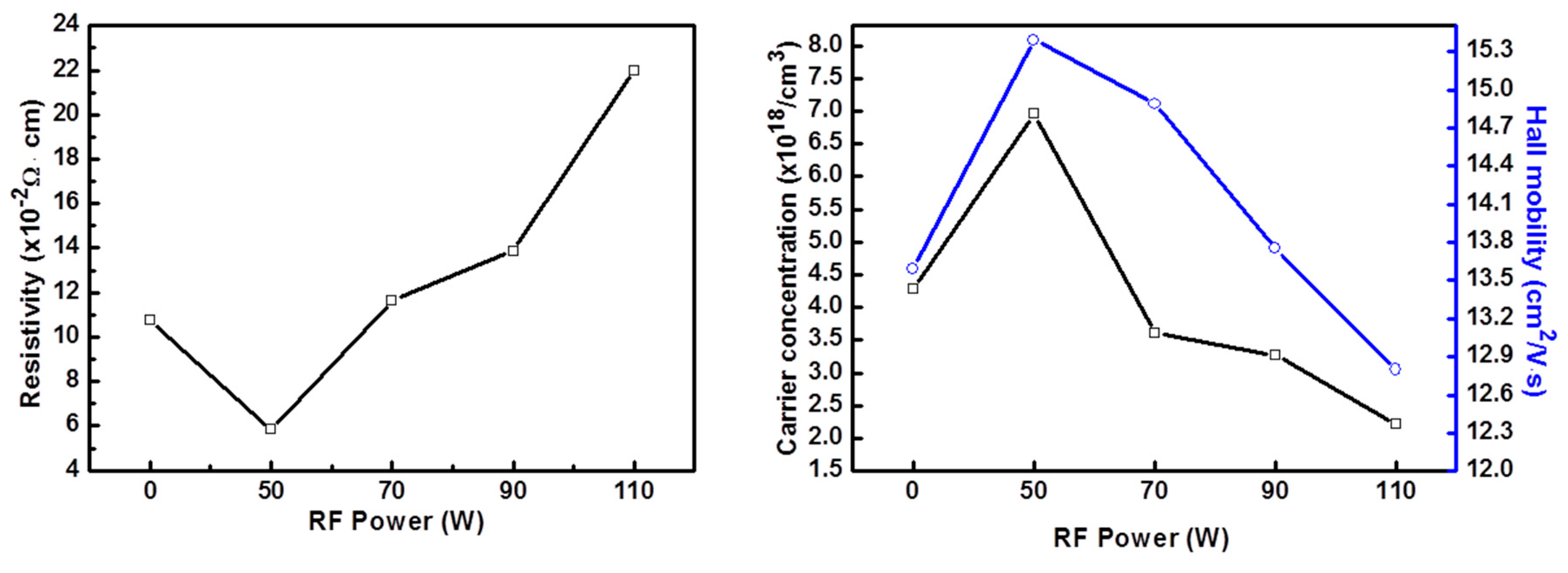
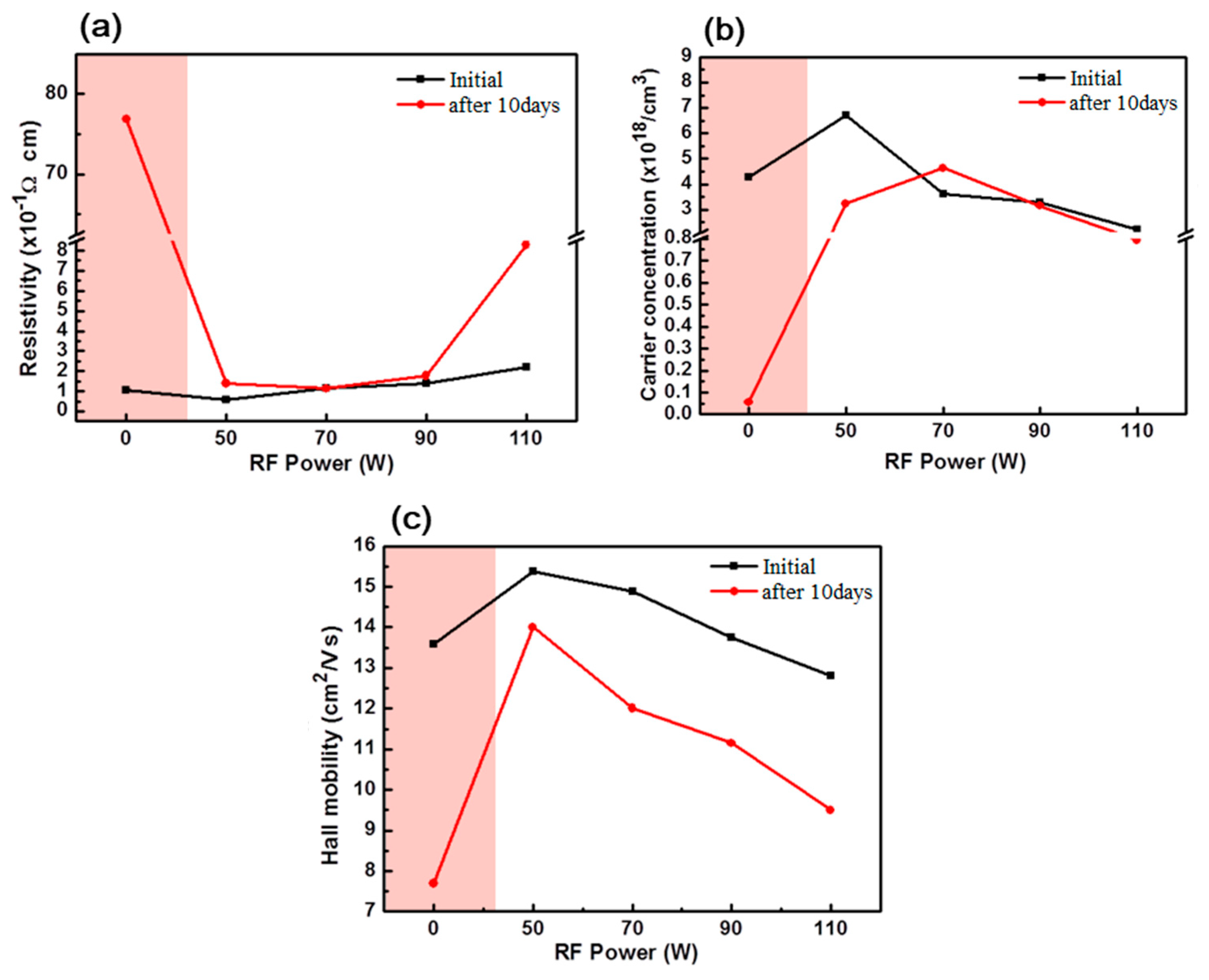
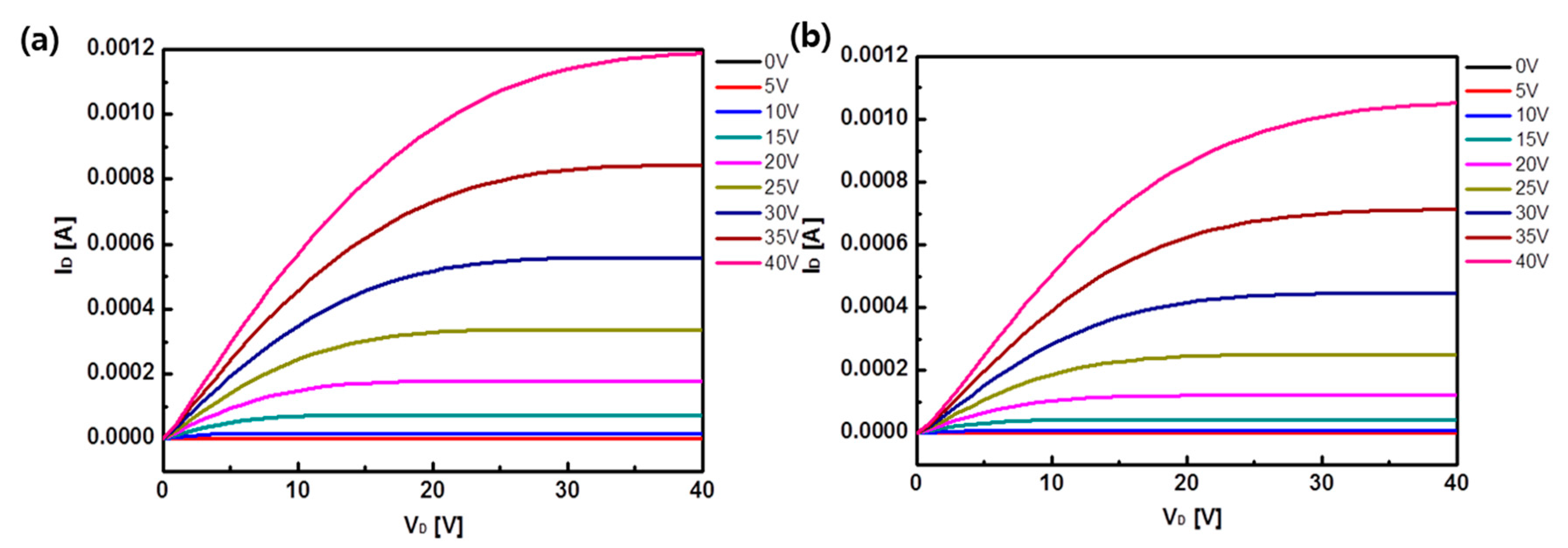
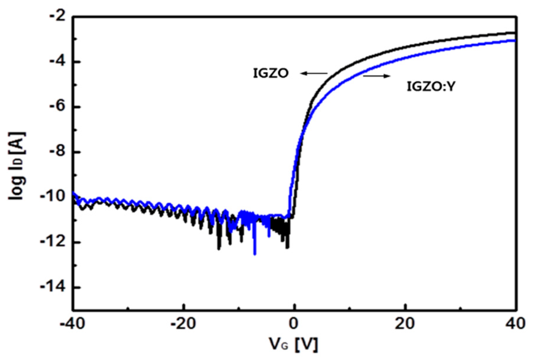
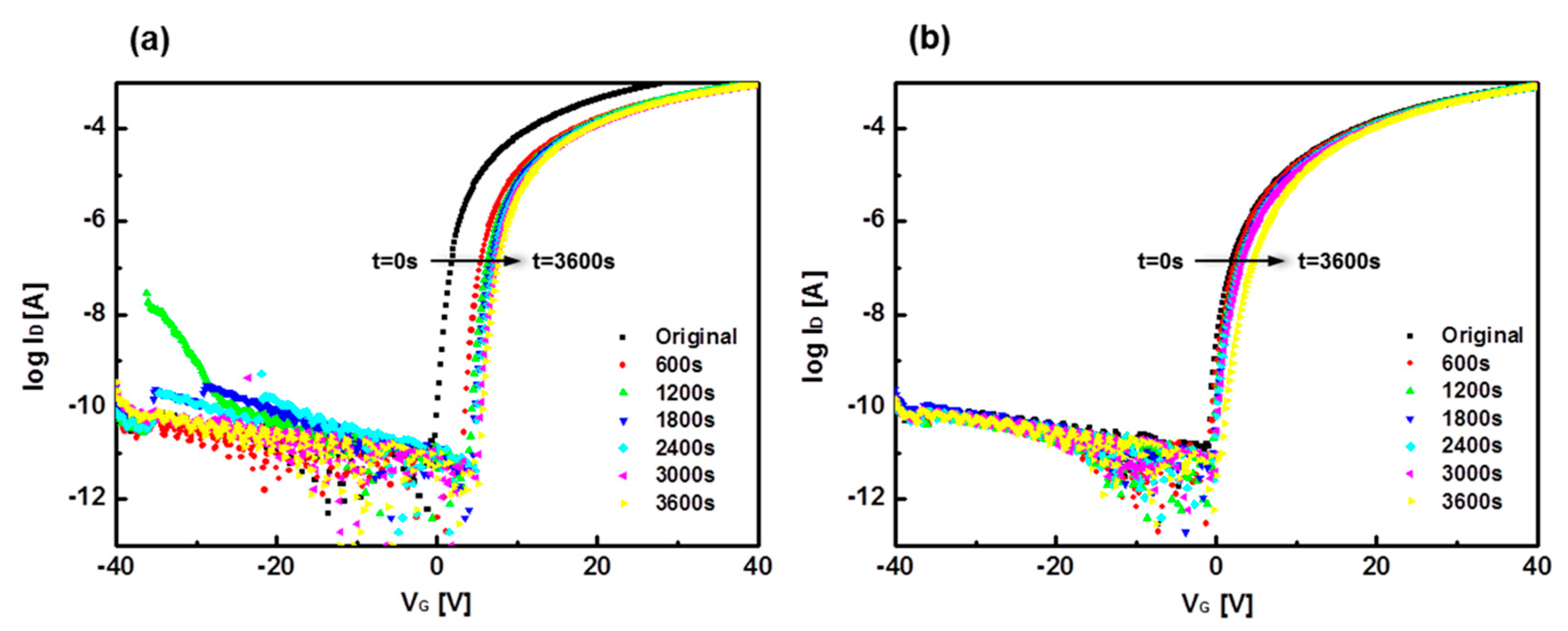
3. Results and Discussion
4. Conclusions
Author Contributions
Funding
Conflicts of Interest
References
- Tanabe, T.; Amano, S.; Miyake, H.; Suzuki, A.; Komatsu, R.; Koyama, J.; Yamazaki, S.; Okazaki, K.; Katayama, M.; Matsukizono, H.; et al. New threshold voltage compensation pixel circuits in 13.5-inch Quad full high definition OLED display of crystalline In–Ga–Zn-Oxide FETs. In Proceedings of the SID Symposium Digest, Boston, MA, USA, 3–8 June 2012; pp. 88–91. [Google Scholar]
- Yamaguchi, H.; Ueda, T.; Miura, K.; Saito, N.; Nakano, S.; Sakano, T.; Sugi, K.; Amemiya, I.; Hiramatsu, M.; Ishida, A. 74.2L: Late-news paper: 11.7-inch flexible AMOLED display driven by a-IGZO TFTs on plastic substrate. In Proceedings of the SID Symposium Digest, Boston, MA, USA, 3–8 June 2012; Volume 43, pp. 1002–1005. [Google Scholar]
- Wallace, R.M.; Wilk, G. Alternative gate dielectrics for microelectronics. MRS Bull. 2002, 27, 186–191. [Google Scholar] [CrossRef]
- Yabuta, H.; Sano, M.; Abe, K.; Aiba, T.; Den, T.; Kumomi, H.; Nomura, K.; Kamiya, T.; Hosono, H. High-mobility thin-film transistor with amorphous InGaZnO4 channel fabricated by room temperature RF-magnetron sputtering. Appl. Phys. Lett. 2006, 89, 112123. [Google Scholar] [CrossRef]
- Kronemeijer, A.J.; Katsouras, I.; Poodt, P.; Akkerman, H.; Van Breemen, A.; Gelinck, G. Flexible a-IGZO TFT technology: New developments applications. In Proceedings of the 25th International Workshop on Active-Matrix Flatpanel Displays and Devices (AM-FPD), Kyoto, Japan, 3–6 July 2018. [Google Scholar]
- Wong, M.; Wang, S.; Feng, Z.; Bebiche, S.; Lu, L.; Kwok, H.S. Elevated-metal metal-oxide (EMMO) thin-film transistor with fluorinated indium-gallium-zinc oxide channel. In Proceedings of the International Display Manufacturing Conference (IDMC), Taipei, Taiwan, 20–22 September 2017. [Google Scholar]
- Seok, M.J.; Choi, M.H.; Mativenga, M.; Geng, D.; Kim, D.Y.; Jang, J. A full-swing a-IGZO TFT-based inverter with a top-gate-bias-induced depletion load. IEEE Electron Device Lett. 2011, 32, 1089–1091. [Google Scholar] [CrossRef]
- Nomura, K.; Ohta, H.; Takagi, A.; Kamiya, T.; Hirano, M.; Hosono, H. Room-temperature fabrication of transparent flexible thin-film transistors using amorphous oxide semiconductors. Nature 2004, 432, 488–492. [Google Scholar] [CrossRef] [PubMed]
- Hosono, H. Recent progress in transparent oxide semiconductors: Materials and device application. Thin Solid Films 2007, 515, 6000–6014. [Google Scholar] [CrossRef]
- Deng, Y.; Li, Z.; Huang, G.; Zhang, Q.; Luo, C.; Yao, J.; Qin, S. Research on the effects of different doping methods on top-Gate IGZO TFT. In Proceedings of the SID Symposium Digest of Technical Papers, Guangzhou, China, 10–12 April 2018; pp. 79–81. [Google Scholar]
- Kim, S.J.; Kim, H.T.; Choi, J.H.; Chung, H.K.; Cho, S.M. Fabrication of amorphous IGZO thin film transistor using self-aligned imprint lithography with a sacrificial layer. Appl. Phys. Lett. 2018, 112, 152104. [Google Scholar] [CrossRef]
- Kim, H.-R.; Yang, J.-H.; Kim, G.-H.; Yoon, S.-M. Flexible thin-film transistors with vertical In–Ga–Zn–O channel using atomic-layer deposition on poly(ethylene naphthalate) substrate. In Proceedings of the 25th International Workshop on Active-Matrix Flatpanel Displays and Devices (AM-FPD), Kyoto, Japan, 3–6 July 2018. [Google Scholar]
- Duan, M.; Zhang, S.; Ren, C.; Zhang, L.; Shao, Y. Impact of sputtering power of source/drain metal on performances of a-IGZO thin film transistors fabricated using wet back-channel-etch process. In Proceedings of the 2017 IEEE International Conference on Electron Devices and Solid-State Circuits (EDSSC), Hsinchu, Taiwan, 18–20 October 2017. [Google Scholar]
- Chen, Y.-C.; Chang, T.-C.; Li, H.-W.; Chen, S.-C.; Chung, W.-F.; Chen, Y.-H.; Tai, Y.-H.; Tseng, T.-Y.; Yeh, F.-S. Surface states related the bias stability of amorphous In–Ga–Zn–O thin film transistors under different ambient gasses. Thin Solid Films 2011, 520, 1432–1436. [Google Scholar] [CrossRef]
- Lee, K.-H.; Jung, J.S.; Son, K.S.; Park, J.S.; Kim, T.S.; Choi, R.; Jeong, J.K.; Kwon, J.-Y.; Koo, B.; Lee, S. The effect of moisture on the photon-enhanced negative bias thermal instability in Ga–In–Zn–O thin film transistors. Appl. Phys. Lett. 2009, 95, 232106. [Google Scholar] [CrossRef]
- Su, B.-Y.; Chu, S.-Y.; Juang, Y.-D.; Liu, S.-Y. Effects of Mg doping on the gate bias and thermal stability of solution-processed InGaZnO thin-film transistors. J. Alloy. Compd. 2013, 580, 10–14. [Google Scholar] [CrossRef]
- Kwon, Y.; Li, Y.; Heo, Y.W.; Jones, M.; Holloway, P.H.; Norton, D.P.; Park, Z.V.; Li, S. Enhancement-mode thin-film field-effect transistor using phosphorus-doped (Zn,Mg)O channel. Appl. Phys. Lett. 2004, 84, 2685–2687. [Google Scholar] [CrossRef]
- Kamiya, T.; Nomura, K.; Hosono, H. Origins of high mobility and low operation voltage of amorphous oxide TFTs: Electronic structure, electron transport, defects and doping. J. Disp. Technol. 2009, 5, 468–483. [Google Scholar] [CrossRef]
- Minami, T.; Yamamoto, T.; Miyata, T. Highly transparent and conductive rare earth-doped ZnO thin films prepared by magnetron sputtering. Thin Solid Films 2000, 366, 63–68. [Google Scholar] [CrossRef]
- Jeong, J.K.; Jeong, J.H.; Yang, H.W.; Park, J.-S.; Mo, Y.-G.; Kim, H.D. High performance thin film transistors with cosputtered amorphous indium gallium zinc oxide channel. Appl. Phys. Lett. 2007, 91, 113505. [Google Scholar] [CrossRef]
- Nomura, K.; Kamiya, T.; Ohta, H.; Ueda, K.; Hirano, M.; Hosono, H. Carrier transport in transparent oxide semiconductor with intrinsic structural randomness probed using single-crystalline InGaO3(ZnO)5 films. Appl. Phys. Lett. 2004, 85, 1993–1995. [Google Scholar] [CrossRef]
- Kim, G.H.; Jeong, W.H.; Du Ahn, B.; Shin, H.S.; Kim, H.J.; Kim, H.J.; Ryu, M.-K.; Park, K.-B.; Seon, J.-B.; Lee, S.-Y. Investigation of the effects of Mg incorporation into InZnO for high-performance and high-stability solution-processed thin film transistors. Appl. Phys. Lett. 2010, 96, 163506. [Google Scholar] [CrossRef]
- Powell, M.J.; van Berkel, C.; Franklin, A.R.; Deane, S.C.; Milne, W.I. Defect pool in amorphous-silicon thin-film transistors. Phys. Rev. B 1992, 45, 4160–4170. [Google Scholar] [CrossRef]


| Sample | VTH (V) | μsat (cm2 V−1 S−1) | Ion/off Ratio | SS (V/dec) |
|---|---|---|---|---|
| a-IGZO TFT | 3.2 | 10.5 | 5 × 10⁹ | 0.43 |
| a-IGZO:Y TFT | 4.6 | 9.8 | 9 × 10⁹ | 0.52 |
© 2019 by the authors. Licensee MDPI, Basel, Switzerland. This article is an open access article distributed under the terms and conditions of the Creative Commons Attribution (CC BY) license (http://creativecommons.org/licenses/by/4.0/).
Share and Cite
Cho, S.; Kim, S.; Kim, D.; Yi, M.; Byun, J.; Song, P. Effects of Yttrium Doping on a-IGZO Thin Films for Use as a Channel Layer in Thin-Film Transistors. Coatings 2019, 9, 44. https://doi.org/10.3390/coatings9010044
Cho S, Kim S, Kim D, Yi M, Byun J, Song P. Effects of Yttrium Doping on a-IGZO Thin Films for Use as a Channel Layer in Thin-Film Transistors. Coatings. 2019; 9(1):44. https://doi.org/10.3390/coatings9010044
Chicago/Turabian StyleCho, Sanghyun, Seohan Kim, Doyeong Kim, Moonsuk Yi, Junseok Byun, and Pungkeun Song. 2019. "Effects of Yttrium Doping on a-IGZO Thin Films for Use as a Channel Layer in Thin-Film Transistors" Coatings 9, no. 1: 44. https://doi.org/10.3390/coatings9010044
APA StyleCho, S., Kim, S., Kim, D., Yi, M., Byun, J., & Song, P. (2019). Effects of Yttrium Doping on a-IGZO Thin Films for Use as a Channel Layer in Thin-Film Transistors. Coatings, 9(1), 44. https://doi.org/10.3390/coatings9010044