Article

Effects of Annealing on Residual Stress in Ta2O5 Films Deposited by Dual Ion Beam Sputtering

1
School of Materials Science & Engineering, Dalian University of Technology, Dalian 116024, China
2
Key Laboratory of Chemical Lasers, Dalian Institute of Chemical Physics, Chinese Academy of Sciences, Dalian 116023, China
*
Authors to whom correspondence should be addressed.
Coatings 2018, 8(4), 150; https://doi.org/10.3390/coatings8040150
Submission received: 16 March 2018 / Revised: 16 April 2018 / Accepted: 16 April 2018 / Published: 20 April 2018
(This article belongs to the Special Issue Applications of Optical Thin Film Coatings)

Abstract

:
Optical coatings deposited by the dual ion beam sputtering (DIBS) method usually show high compressive stress, which results in severe wavefront deformation of optical elements. Annealing post-treatment has been widely used to control the residual stress of optical coatings. However, the effect of annealing on the stress of Ta2O5 films deposited by the IBS method has not been reported in detail. In this study, different thicknesses of Ta2O5 films were deposited by IBS and annealed at different temperatures from 473 to 973 K in air, and the effect of annealing on the stress of Ta2O5 films was investigated. The as-deposited Ta2O5 films deposited by IBS show high compressive stress, which are about 160 MPa. The compressive stress decreases linearly with the increasing temperature, and the wavefront deformation of Ta2O5 films increases linearly with film thickness (within 20 μm) at the same annealing temperature. When the temperature rises to 591 K, Ta2O5 films with zero-stress can be obtained. Ta2O5 films show tensile stress instead of compressive stress with further increasing annealing temperature, and the tensile stress increases with increasing temperature. Meanwhile, with the increasing annealing temperature, the refractive index of Ta2O5 film decreases, indicating the decreasing packing density. The atomic force microscope (AFM) test results show that surface roughness of Ta2O5 films slowly increases with the increasing of annealing temperature. Moreover, X-ray photoelectron spectroscopy (XPS) analysis shows that the Ta in Ta2O5 films can be further oxidized with increasing annealing temperature, namely, the absorption of Ta2O5 film can be reduced. X-ray diffraction (XRD) analysis shows that the annealing temperature should be below 923 K to maintain the amorphous structure of the Ta2O5 film.

1. Introduction

The residual stress introduced during optical thin film deposition [1,2,3] has been paid great attention in past decades, and many efforts have already been made on the research of the relationship between the residual stress and process parameters of different deposition methods [4,5,6]. The performance of optical coating elements is affected greatly by the residual stress in thin films, such as spectroscopic and mechanical reliability [7,8], and the surface figure. Taking dense wavelength division multiplexing (DWDM) filters (more than 150 layers in all) as an example, the multi-layers will suffer the surface distortion of optics, even layers flaking or fracturing due to the residual stress accumulation [4,9]. Therefore, residual stress must be finely controlled in many frontier optical application fields.
It is well known that dual ion beam sputtering (DIBS) technology is an effective coating deposition method to fabricate optical films with ultra-low loss, high packing density and a high laser-induced damage threshold (LIDT) [4,10,11]. The high-quality optical coating elements fabricated by IBS have been widely applied in many important engineering projects, such as the National Ignition Facility (NIF), Laser Interferometer Gravitational-wave Observatory (LIGO), etc. [12,13,14,15]. However, the main drawback of IBS technology is the high compressive stress of films generated in the deposition process [15,16], which result in severe surface distortion of optical elements. In order to attain a high quality of optical coating elements with a good surface figure and good optical performance, it is very necessary to study the stress behavior of single layers, including the relationship between the residual stress and process parameters [17].
Due to good optical properties in the visible and near-infrared regions, thermal and chemical stability, and high refractive index, Ta2O5 has been widely used as a high refractive index material in fine optical coatings [18,19]. Many studies show that Ta2O5 films fabricated by IBS exhibit high compressive stress [20,21]. Annealing treatments are an effective method to reduce film stress considerably, which has already been employed to control the deformation of the HfO2 films [22]. Yoon reported that annealing treatments can reduce the stress of Ta2O5 films deposited on silicon substrate when the annealing temperature is below 673 K [23]. However, the effect of annealing on the stress of Ta2O5 films deposited on a quartz substrate has not been systematically investigated and the annealing temperature point for zero-stress has been rarely obtained.
In the present work, the effect of annealing treatments on stress behaviors of Ta2O5 films deposited by IBS technology was systematically investigated. Firstly, the crystalline structure of the Ta2O5 films was analyzed by X-ray diffraction (XRD). Given the boundary defect effect, annealing temperature should be below 923 K to maintain the amorphous structure of the Ta2O5 film. Secondly, the stress behavior of Ta2O5 films with different annealed thicknesses at different temperatures is studied in detail and a relationship among the stress, layer thickness, and annealing temperature is obtained. Then, the optical properties and microstructure of the Ta2O5 films annealed at different temperatures were investigated. Finally, surface chemistry analysis was carried out by X-ray photoelectron spectroscopy (XPS). This work will demonstrate that the residual stress of Ta2O5 layers can be successfully manipulated by annealing treatments. At the same time, annealing treatments can guarantee Ta2O5 layers with smooth surfaces and even improve the optical properties and stoichiometry. The results obtained in this study can offer technical feasibility for residual stress control and compensation of Ta2O5 films.

2. Experimental Details

Ta2O5 films were deposited by a dual ion beam sputtering system equipped with a 16 cm primary ion beam source and a 12 cm assisted ion beam source. The target material is tantalum (99.99%). The base pressure was up to 8 × 10⁻⁷ Torr. The deposition temperature was maintained at 353 K during the deposition process. The target O2 gas was introduced on the target surface and the gas flow was 30 sccm. The beam voltage and current of 16 cm primary ion beam source were set at 1250 V and 600 mA, respectively, and at 250 V and 200 mA for the 12 cm RF assisted ion source. Ar (25 sccm) and O2 (25 sccm) gas were introduced into the primary and assisted ion source. The deposition rates were 0.20 nm/s for Ta2O5 film. All samples were deposited on Φ 25.4 mm × 1 mm fused silica substrates (synthetic fused silica glass AQ series, manufactured by Asahi Glass Co., Ltd., Tokyo, Japan.
The annealing experiments were performed in a Nabertherml oven (Lilienthal, Germany) at temperatures from 573 to 973 K [17,24,25]. For all cases, the annealing treatment was performed for 10 h in air. The ramp-up rate was controlled at 2 °C/min and then the samples were free-cooled in the furnace. Detailed experiment results after annealing treatment are shown in Table 1.
The transmission spectra were measured by a Perkin Elmer Lambda 950 spectrophotometer (Waltham, MA, USA). Based on the transmission spectra, the refraction index was obtained by fitting the spectra according to the Lorentzian multioscillator model [27]. The accuracy in n determination is of the order of ±0.005 [16]. The packing density (P) was related to refractive index of Ta2O5 film and calculated by the following equation [26]:
n f = P n s + ( 1 P ) n v
where ns and nv are the refractive indices of the solid part of the film and the vacancies, respectively. Assuming an empty pore (nv ≈ 1), the packing density can be obtained and shown in Table 1.
X-ray photoelectron spectroscopy (XPS, Thermo Scientific ESCALAB 250Xi, Waltham, MA, USA) was used to determine the surface chemistry of the films. The X-ray radiation was the monochromatic Al Kα line; the X-ray spot size and the take-off angle were 0.8 mm and 45°, respectively. The survey spectra were recorded with pass energy of 187.85 eV and an energy step of 0.8 eV. The crystalline structure of the films was measured by X-ray diffractometer (XRD, PANalytical, Empyean, Almelo, The Netherlands) with scanning angles from 20° to 80°. The measured data were analyzed by HighScorePlus Software (version 3.0.5).
An interferometer (Fizeau, GPI-XP, Zygo, Middlefield, CT, USA) was employed to measure the reflective wavefront deformation (RWD) before and after deposition and annealing treatments. Then the residual stress of films can be calculated by the Stoney formula [28]:
σ = E s t s 2 6 ( 1 v s ) t f R
where σ is the residual stress of the film; Es and v s are the elastic modulus and Poisson ratio of the substrate, respectively. For fused silica substrates, ES = 71.7 GPa and νs = 0.17 were used in the calculation [29]; R is the radius of curvature of the substrate; Ds is the diameter of the substrate; ts is the thickness of the substrate; and tf is the thickness of the film. Figure 1 shows the schema of the substrate surface. Since θ is small enough due to the flat surface, the following equation can be deduced from the geometry:
D 2 R θ
P V = h = R ( 1 cos θ ) = 2 R sin 2 ( θ 2 ) D 2 8 R
The power value change (ΔPV), which represents the variation of the RWD, meets the following equation. ΔPV is the value of the surface figure change which can be measured by an interferometer:
Δ P V = P V 1 P V 2 = D 2 8 ( 1 R 1 1 R 2 )
Thus, the Stoney equation can be written as follows:
σ = 4 E s 3 ( 1 v s ) t s 2 D s 2 Δ P V t f
In the present study, negative and positive stress values represent tensile and compressive stress, respectively. The accuracy in the PV value determination is of the order of 0.05 (1/20λ, λ = 632.8 nm, is the detector wavelength).
A scanning atomic force microscope (AFM, di Digital Instruments, D3100, Veeco Metrology Group, Plainview, NY, USA) was utilized to characterize the surface morphology. The scanning mode was configured as contact, with a scanning rate of 1 Hz and high vertical resolution of ±0.025 nm. A region with the size of 2.5 µm × 2.5 µm was selected for the characterization of the specimen. The obtained images were processed to remove background signals and to extract results, such as surface roughness (Rms) and topographic profiles. The accuracy in Rms roughness determination is of the order of ±0.025 nm.

3. Results and Discussion

The XRD patterns of Ta2O5 films are shown in Figure 2. It can be seen that there are no identifiable diffraction peaks in Ta2O5 films annealed below 923 K and the peak intensity varies slightly with the increase of the annealing temperature. Namely, Ta2O5 films annealed below 923 K all stay in amorphous structure. When the annealing temperature rises to 933 K, the Ta2O5 film is no longer amorphous and crystallizes to a hexagonal phase. Consequently, the temperature for phase conversion is between 923 and 933 K. It is a common view that a better laser-induced damage threshold (LIDT) could be obtained for amorphous optical films because it is easier to realize diffusion of the impurities in crystalline structured films, and this causes a local impurity region which is a grain boundary defect in the structure [11]. We also know that stress in the thin films can be introduced after phase conversion because of the boundary defect. Thus, according to the above results, it can be concluded that the annealing temperature should be below 923 K to maintain the amorphous structure of the Ta2O5 film.
Figure 3a gives the relationship curve between RWD and the thickness of Ta2O5 films annealed at different temperatures. As can be seen from Figure 3a, the RWD and film thickness exhibited a linear relationship within 20 μm at all annealing temperatures, which is in accordance with previous reports [6]. The RWD caused by the Ta2O5 films are all negative when annealed below 573 K. With the increase of the annealing temperature, the RWD value increases. When the annealing temperature rises to a certain point, the Ta2O5 films without wavefront deformation can be obtained. With a further increase in the annealing temperature, RWD converts to be positive and become larger and larger with increasing annealing temperature. We use the linear regression mode to fit the experimental data and the relationship between RWD and the layer thickness (tf) can be summarized as follows:
RWD T = k T t f + C T
where k T is the slope of the function, which is related to the annealing temperature. As can be seen in Figure 3a, for different annealing temperatures, k T is completely different. C T is the constant term. We list the linear regression fitting results for each of the annealing temperatures in Table 2.
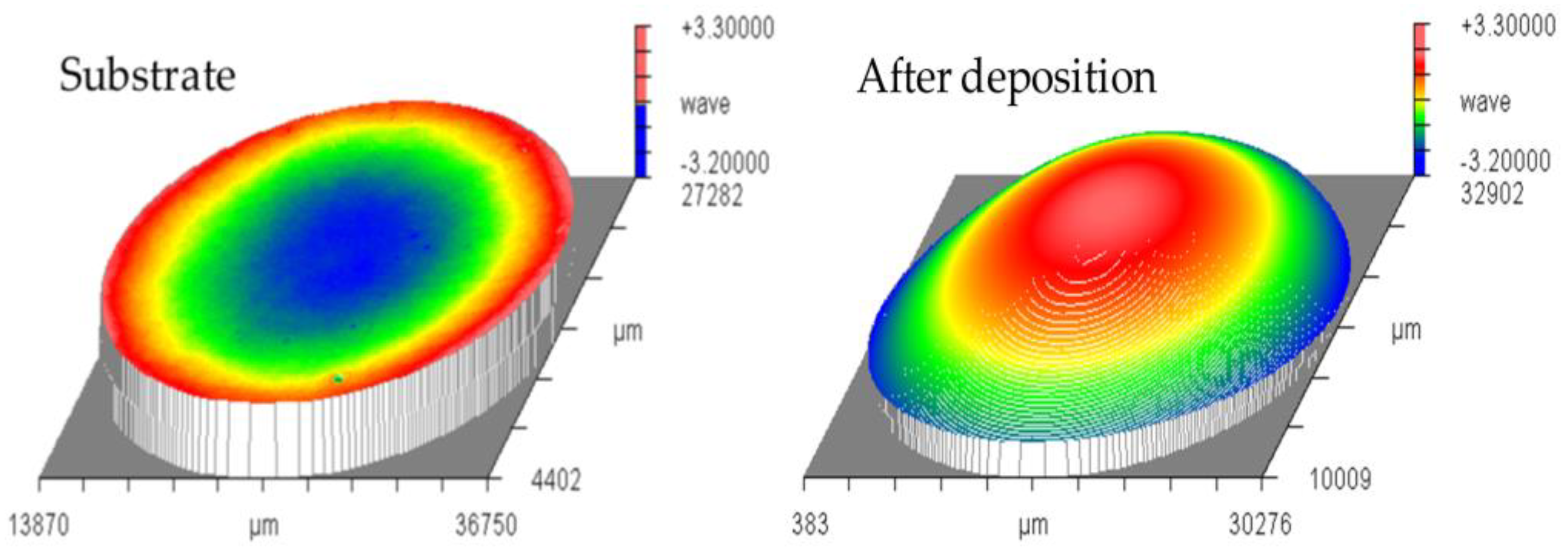
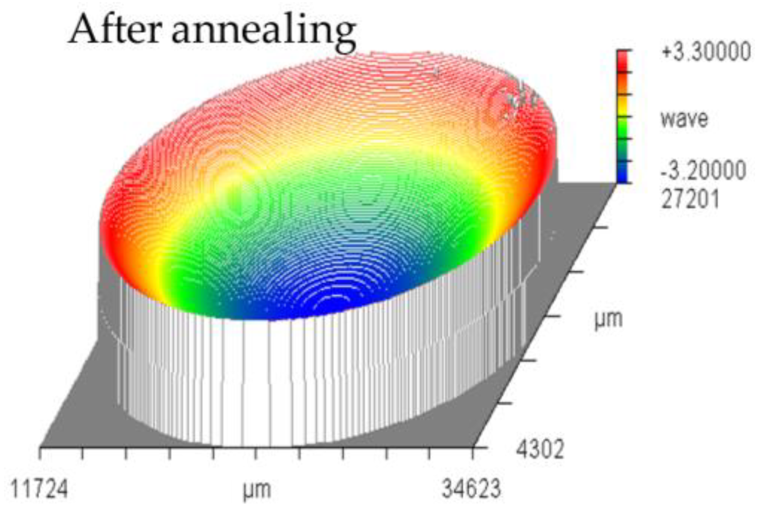
In order to make the relationship clear between the annealing temperature and the RWD of Ta2O5 films with different thicknesses, the data shown in Figure 3a is redescribed in Figure 3b. As can be seen from Figure 3b, all the curves with different thickness intersect at a certain annealing temperature point. This means that the negative RWD of Ta2O5 films with different thicknesses all convert to positive RWD after a certain temperature threshold. This temperature threshold can be predicted as show below. Figure 4 shows the surface figures of substrate and Ta2O5 film on fused silica before and after annealing treatment (annealed at 773 K). Before deposition, the substrate was polished to have a good plane of small surface tolerance. The as-deposited Ta2O5 films show high compressive stress, whereas the annealed Ta2O5 films have high tensile stress, as is presented in Figure 4 (more details in Supplementary Materials, Figure S1). According to the Stoney formula, the residual stress of the Ta2O5 films are calculated and shown in Figure 3c. As can be seen in Figure 3c, the final stress of the Ta2O5 films strongly depend on the annealing temperature, and the residual stress decreases with the annealing temperature linearly between 473 and 773 K. At a certain temperature threshold, zero stress of Ta2O5 films can be obtained, and with further improving the annealing temperature, compressive stress of Ta2O5 films begins to convert to tensile one. This interesting result agrees with Martin Bischoff’s report on HfO2 film [16]. Packing density represents the porosity of thin films. In this study, the varied packing density (see Table 1), as well as the surface roughness, is related to the modification of the microstructure of the Ta2O5 film due to annealing, which is furthermore connected with a release of the film stress.
For further study, according to Figure 3a and Table 2, the relationship between k T and the annealing temperatures is plotted in Figure 3d. It can be seen that k T at different annealing temperatures exhibits a linear relationship. Thus, a zero-stress temperature point for Ta2O5 films with different thicknesses can be predicted. We also fit the slope curve using the linear regression mode and the relationship between the slope ( k T ) and the annealing temperature (T) can be summarized as follows:
k T = 2.84 + 4.85 × 10 3 T
On the basis of calculation, the zero-stress temperature point is 591 K. Consequently, it can be concluded that the compressive stress of Ta2O5 films with different thicknesses converts to tensile stress when the annealing temperature is 591 K.
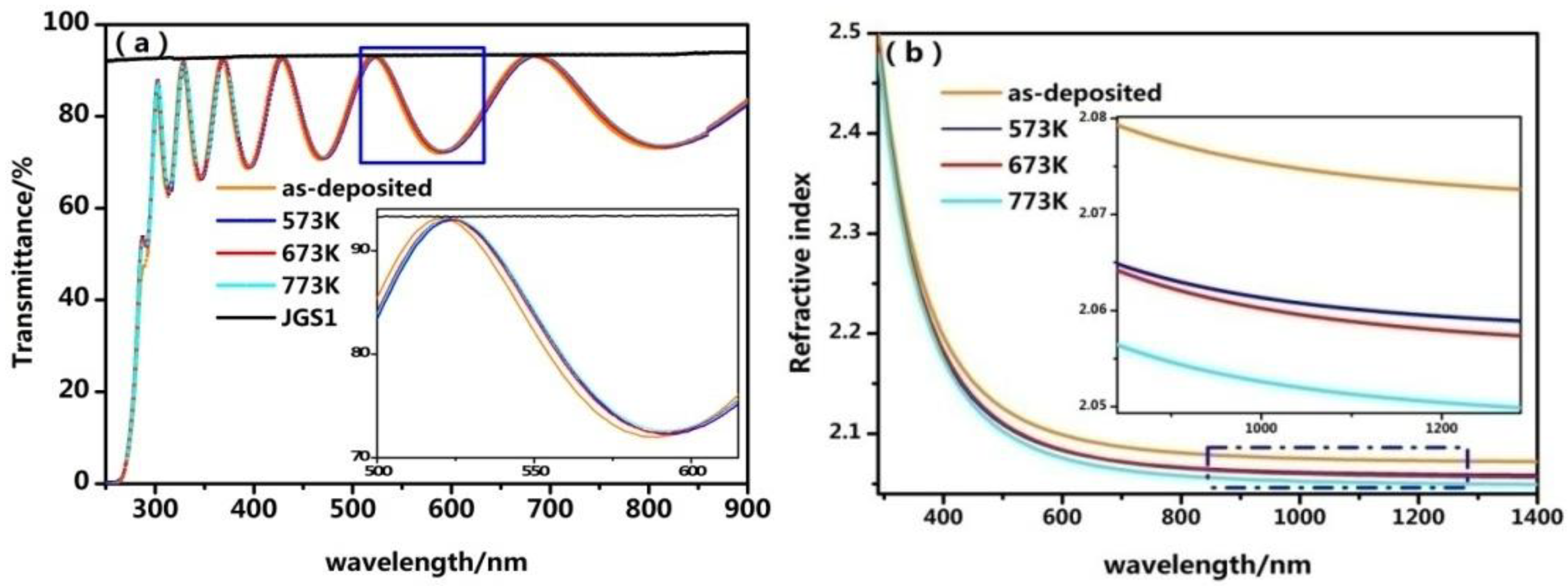
Considering the application in optical systems, Ta2O5 films after annealing treatments should not only have low residual stress, but also have good optical properties. In order to investigate the effect of annealing temperature on the refractive index and microstructure, the Ta2O5 films with thicknesses of 500 nm annealed at different annealing temperatures were characterized. Figure 5 shows the transmittance curves of the Ta2O5 films with thicknesses of 500 nm annealed at different annealing temperatures. As shown in Figure 5a, the transmittance spectra of the Ta2O5 films shift toward the long-wavelength region and the minimum value increases with the increase of the annealing temperature, which indicates that the optical thickness of Ta2O5 films increases and the refractive index decreases with the increase of the annealing temperature. This would mean the physical thickness of films increase. The same results have been discussed in [25]. The change of coating thickness and index after annealing mainly results from the rearrangement of the microstructure. Figure 5b shows the refractive index of the 500-nm Ta2O5 films annealed at different temperatures. As can be seen, the refractive index obviously decreases after annealing treatments. According to the relationship between the refraction index and the packing density, this means that the packing density decreases with the increase of the annealing temperature. These results are in agreement with the commonly-reported relationship between the optical constant and annealing temperature [16].
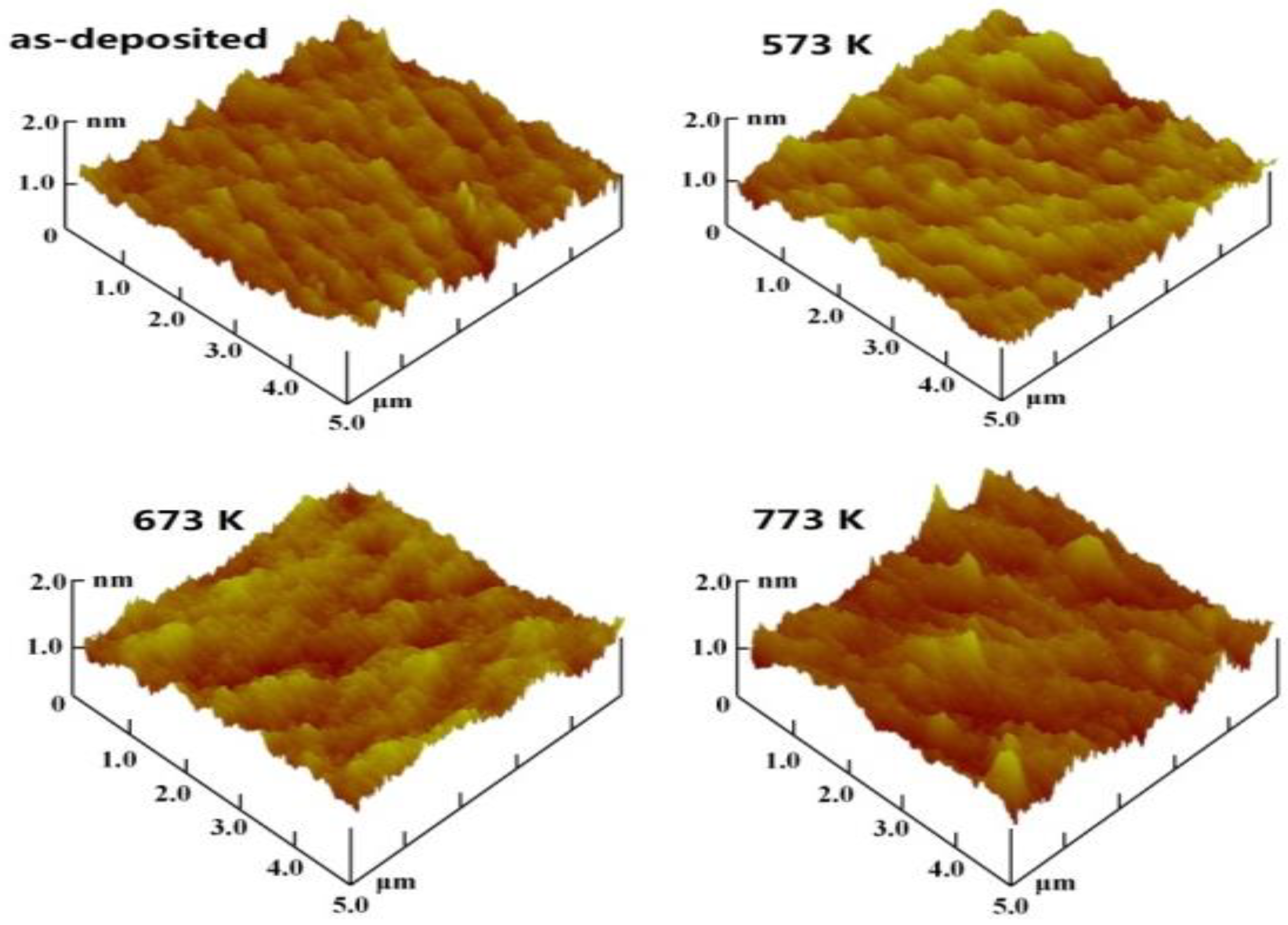
Figure 6 shows the AFM images of the as-deposited Ta2O5 films with a thickness of 500 nm annealed at different temperatures. The measurement results are listed in Table 1. From Table 1, we conclude that the surface roughness of Ta2O5 films slowly increases with the increase of the annealing temperature. When the annealing temperature rises to 773 K, the surface roughness of the Ta2O5 films increase to 0.24 nm. The probable reason for the increased Rms roughness after annealing is that annealing treatments offer the atoms enough activation energy to diffuse to the site with the lower surface energy in the horizontal direction. The atoms’ rearrangement leads to a rougher surface. In this experiment, it shows that the Ta2O5 film annealed at 773 K still has a small Rms roughness, indicating that annealing treatments can lead to few structural defects on the surface of the film.
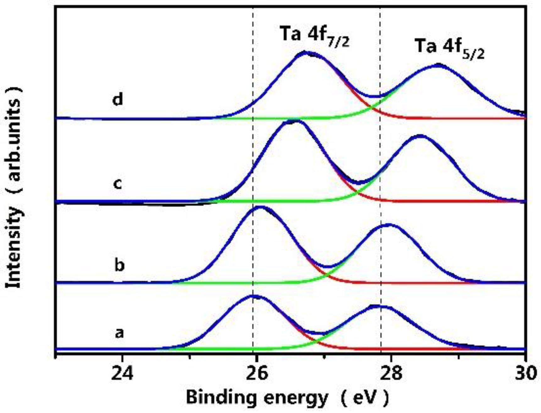
X-ray photoelectron spectroscopy (XPS) was carried out upon Ta2O5 film surfaces and the Ta 4f spectra with constituent satellite peaks are illustrated in Figure 7. Each oxidation state of Ta is represented by a Ta 4f7/2 to Ta 4f5/2 doublet. The energy separation of the doublet lines is always fixed to 1.9 eV and the area ratio is about 1.33. As for as-deposited film, Ta 4f7/2 to Ta 4f5/2 peaks located at 25.94 and 27.83 eV are observed. Deep oxidation of Ta2O5 film is also certified in the oxygen XPS spectra (Supplementary Materials, Figure S2–S4) and oxygen peaks also shifted to higher binding energy with the increase of the annealing temperature. Qualitatively from XPS spectra (Figure 7), the binding energy of the Ta 4f7/2 to Ta 4f5/2 doublet moves to the higher energy side when the annealing temperature increases, which indicates the Ta is oxidized more deeply. It can be concluded that a moderate annealing can repair oxygen vacancies that exist within Ta2O5 amorphous films. Optical films benefit from this process demonstrating the significant reduction of optical adsorption (see Table 1 and Table S1).

4. Conclusions

Ta2O5 films with different thicknesses were deposited by IBS and annealed at different temperatures from 473 to 973 K in air. After annealing, the wavefront deformation of Ta2O5 films linearly increases with film thickness (within 20 μm) at the same annealing temperature. The compressive stress linearly decreases with the increasing temperature. When the temperature rises to 591 K, Ta2O5 films with zero stress can be obtained. To further increase the annealing temperature, Ta2O5 films show tensile stress instead of compressive stress. The tensile stress increases with the increasing temperature.
Meanwhile, annealing treatments can improve the film stoichiometric ratio leading to the reduction of absorption. XRD results show that in order to avoid grain boundary defects, the annealing temperature should be below 923 K to maintain the amorphous structure of the Ta2O5 film. Annealing treatment is in favor of reducing the refractive index and increasing the surface roughness. However, the films after annealing treatments still maintain the high surface quality and optical properties, and meet the requirements in optical applications, even with a little change in the refractive index and the surface roughness.

Supplementary Materials

The following are available online at https://www.mdpi.com/2079-6412/8/4/150/s1, Figure S1: The surface figure of Ta2O5 films on fused silica before deposition, after deposition, and after annealing treatments at various temperatures, Figure S2: XPS survey spectra of Ta2O5 films under various annealing temperature, Figure S3: XPS spectra of oxygen (O 1s) with satellite peaks under various annealing temperature, Figure S4: The surface figure of Ta2O5 films on fused silica before deposition, after deposition, and after annealing treatments at various temperatures, Table S1: O/Ta ratio of Ta2O5 films based on XPS survey spectra.

Acknowledgments

This work was sponsored by the National Natural Science Foundation of China (grant no. 61505209), the Scientific Research Foundation of Chinese Academy of Sciences. Youth Innovation Promotion Association of CAS (grant no. 2017230), and the Dalian Science and Technology Star Program.

Author Contributions

Mingliang Huang and Gang Li conceived and designed the experiments; Qipeng Lv performed the experiments; Songwen Deng and Shaoqian Zhang analyzed the data; Faquan Gong, Feng Wang, and Yanwei Pan contributed reagents/materials/analysis tools; Qipeng Lv and Shaoqian Zhang wrote/revised the manuscript; and Yuqi Jin participated in the study design.

Conflicts of Interest

The authors declare no conflict of interest.

References

  1. Sun, R.C.; Tisone, T.C.; Cruzan, P.D. The origin of internal stress in low−voltage sputtered tungsten films. J. Appl. Phys. 1975, 46, 112–117. [Google Scholar] [CrossRef]
  2. Hsueh, C.H. Thermal stresses in elastic multilayer systems. Thin Solid Films 2002, 418, 182–188. [Google Scholar] [CrossRef]
  3. Ennos, A.E. Stresses developed in optical film coatings. Appl. Opt. 1966, 5, 51–61. [Google Scholar] [CrossRef] [PubMed]
  4. Yoon, S.G.; Kim, Y.T.; Kim, H.K.; Kim, M.J.; Lee, H.M.; Yoon, D.H. Comparision of residual stress and optical properties in Ta2O5 thin films deposited by single and dual ion beam sputtering. Mater. Sci. Eng. B 2005, 118, 234–237. [Google Scholar] [CrossRef]
  5. Wang, J.; Maier, R.L. Correlation between mechanical stress and optical properties of SiO2/Ta2O5 multilayer UV narrow-bandpass filters deposited by plasma ion-assisted deposition. In Advances in Thin-Film Coatings for Optical Applications II, Proceedings of Optics and Photonics 2005, San Diego, CA, USA, 31 July–4 August 2005; Fulton, M.L., Kruschwitz, J.D.T., Eds.; SPIE: Bellingham, WA, USA, 2005; p. 58700E. [Google Scholar]
  6. Deng, S.W.; Wang, F.; Liu, S.F.; Li, G.; Sun, L.; Jin, Y.Q. Residual stress prediction and control of Ta2O5/SiO2 multilayer based on layer structure designing. Chin. Opt. Lett. 2013, 11, S10701. [Google Scholar] [CrossRef]
  7. Atanassova, E.; Tyuliev, G.; Paskaleva, A.; Spassov, D.; Kostov, K. XPS study of N2 annealing effect on thermal Ta2O5 layers on Si. Appl. Surf. Sci. 2004, 225, 86–99. [Google Scholar] [CrossRef]
  8. Atanassova, E.; Dimitrova, T.; Koprinarova, J. AES and XPS study of thin RF-sputtered Ta2O5 layers. Appl. Surf. Sci. 1995, 84, 193–202. [Google Scholar] [CrossRef]
  9. Teixeira, V. Residual stress and cracking in thin PVD coatings. Vacuum 2002, 64, 393–399. [Google Scholar] [CrossRef]
  10. Brown, J.T. Center wavelength shift dependence on substrate coefficient of thermal expansion for optical thin-film interference filters deposited by ion-beam sputtering. Appl. Opt. 2004, 43, 4506–4511. [Google Scholar] [CrossRef] [PubMed]
  11. Cosar, M.B.; Ozhan, A.E.S.; Aydogdu, G.H. Improving the laser damage resistance of oxide thin films and multilayers via tailoring ion beam sputtering parameters. Appl. Surf. Sci. 2015, 336, 34–38. [Google Scholar] [CrossRef]
  12. Forest, D.; Ganau, P.; Lagrange, B.; Mackowski, J.M.; Michel, C.; Montorio, J.L.; Morgado, N.; Pignard, R.; Pinard, L.; Remillieux, A.I.B.S. Coatings on large substrates: Towards an improvement of the mechanical and optical performances. In Proceedings of the Optical Interference Coatings, Tucson, AZ, USA, 27 June 2004; p. MB7. [Google Scholar]
  13. Martin, I.W.; Nawrodt, R.; Craig, K.; Schwarz, C.; Bassiri, R.; Harry, G.; Hough, J.; Penn, S.; Reid, S.; Robie, R.; et al. Low temperature mechanical dissipation of an ion-beam sputtered silica film. Class. Quant. Grav. 2014, 31, 35019–35030. [Google Scholar] [CrossRef]
  14. Stolz, C.; Weinzapfel, C.; Rogowski, G.T.; Smith, D.; Rigatti, A.; Oliver, J.; Taniguch, J. Status of optical coatings for the national ignition facility. In Proceedings of the Optical Interference Coatings, Banff, AB, Canada, 15 July 2001; p. ThD3. [Google Scholar]
  15. Netterfield, R.P.; Gross, M.; Baynes, F.N.; Green, K.L.; Harry, G.M.; Armandula, H.; Rowan, S.; Hough, J.; Crooks, D.R.M.; Fejer, M.M.; et al. Low mechanical loss coatings for LIGO optics: Progress report. In Advances in Thin-Film Coatings for Optical Applications II, Proceedings of Optics and Photonics 2005, San Diego, CA, USA, 31 July–4 August 2005; Fulton, M.L., Kruschwitz, J.D.T., Eds.; SPIE: Bellingham, WA, USA, 2005; p. 58700H. [Google Scholar]
  16. Bischoff, M.; Nowitzki, T.; Voß, O.; Wilbrandt, S.; Stenzel, O. Postdeposition treatment of IBS coatings for UV applications with optimized thin-film stress properties. Appl. Opt. 2014, 53, A212–A220. [Google Scholar] [CrossRef]
  17. Xu, C.; Xiao, Q.; Ma, J.; Jin, Y.; Shao, J.; Fan, Z. High temperature annealing effect on structure, optical property and laser-induced damage threshold of Ta2O5 films. Appl. Surf. Sci. 2008, 254, 6554–6559. [Google Scholar] [CrossRef]
  18. Qiao, Z.; Pu, Y.; Liu, H.; Luo, K.; Wang, G.; Liu, Z.; Ma, P. Residual stress and laser-induced damage of ion-beam sputtered Ta2O5/SiO2 mixture coatings. Thin Solid Films 2015, 592, 221–224. [Google Scholar] [CrossRef]
  19. Shang, P.; Xiong, S.; Li, L.; Tian, D.; Ai, W. Investigation on thermal stability of Ta2O5, TiO2 and Al2O3 coatings for application at high temperature. Appl. Surf. Sci. 2013, 285, 713–720. [Google Scholar] [CrossRef]
  20. Tien, C.L. Influence of ejection angle on residual stress and optical properties of sputtering Ta2O5 thin films. Appl. Surf. Sci. 2008, 255, 2890–2895. [Google Scholar] [CrossRef]
  21. Tang, C.J.; Jaing, C.C.; Lee, K.S.; Lee, C.C. Residual stress in Ta2O5-SiO2 composite thin-film rugate filters prepared by radio frequency ion-beam sputtering. Appl. Opt. 2008, 47, 167–171. [Google Scholar] [CrossRef]
  22. Stenzel, O.; Wilbrandt, S.; Kaiser, N.; Vinnichenko, M.; Munnik, F.; Kolitsch, A.; Chuvilin, A.; Kaiser, U.; Ebert, J.; Jakobs, S. The correlation between mechanical stress, thermal shift and refractive index in HfO2, Nb2O5, Ta2O5 and SiO2 layers and its relation to the layer porosity. Thin Solid Films 2009, 517, 6058–6068. [Google Scholar] [CrossRef]
  23. Yoon, S.G.; Kang, S.M.; Yoon, D.H. Post-annealing effects on the structural properties and residual stress of Ta2O5 thin films deposited by ion beam sputtering. J. Optoelectron. Adv. Mater. 2007, 9, 1246–1249. [Google Scholar]
  24. Zhao, Y.A.; Wang, Y.J.; Gong, H.; Shao, J.D.; Fan, Z.X. Annealing effects on structure and laser-induced damage threshold of Ta2O5/SiO2 dielectric mirrors. Appl. Surf. Sci. 2003, 210, 353–358. [Google Scholar] [CrossRef]
  25. Xu, C.; Li, D.W.; Fan, H.L.; Deng, J.X.; Qi, J.W.; Yi, P.; Qiang, Y.H. Effects of different post-treatment methods on optical properties, absorption and nanosecond laser-induced damage threshold of Ta2O5 films. Thin Solid Films 2015, 580, 12–20. [Google Scholar] [CrossRef]
  26. Xu, C.; Yang, S.; Zhang, S.; Niu, J.; Qiang, Y.; Liu, J.; Li, D. Temperature dependences of optical properties, chemical composition, structure and laser damage in Ta2O5 films. Chin. Phys. B 2012, 21, 297–305. [Google Scholar] [CrossRef]
  27. Born, M.; Wolf, E. Electromagnetic potentials and polarization. In Principles of Optics; Pergamon: London, UK, 1959; p. 986. [Google Scholar]
  28. Stoney, G.G. The tension of metallic films deposited by electrolysis. Proc. R. Soc. Lond. A 1909, 82, 40–43. [Google Scholar] [CrossRef]
  29. Kičas, S.; Gimževskis, U.; Melnikas, S. Post deposition annealing of IBS mixture coatings for compensation of film induced stress. Opt. Mater. Express 2016, 6, 2236–2243. [Google Scholar] [CrossRef]
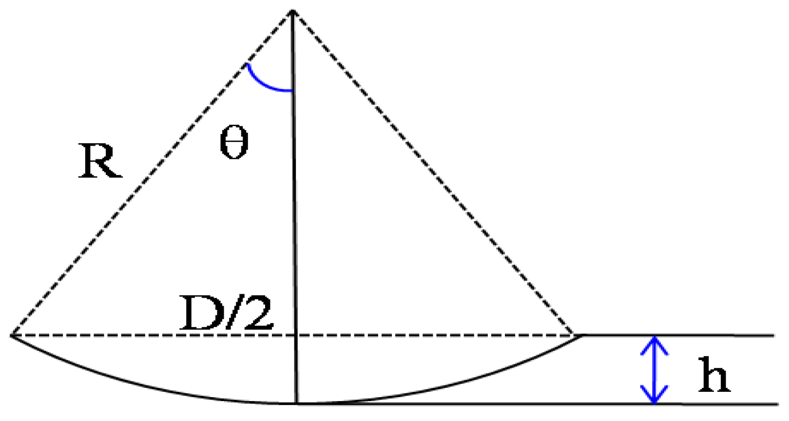
Figure 1. Schema of the substrate surface.
Coatings 08 00150 g001
Figure 2. XRD patterns of Ta2O5 film with a thickness of 500 nm; the crystal phase of Ta2O5 films annealed at different temperatures in the range of 873 to 973 K. When the annealing temperature rises to 973 K, Ta2O5 film converts from an amorphous to a hexagonal crystalline phase.
Coatings 08 00150 g002
Figure 3. (a) The relationship curve between RWD and thickness of Ta2O5 film annealed at different temperatures; (b) the relationship between temperature and the RWD of Ta2O5 films with different thicknesses; (c) the stress of the Ta2O5 films with thicknesses of 500 nm annealed at different temperatures; annealing temperatures are set at 473 K, 523 K, 573 K, 623 K, 673 K, 723 K, and 773 K, respectively; and (d) the relationship between kT (slope) and annealing temperature. kT, which is related to the annealing temperature, is the slope of Equation (7) and described using Equation (8).
Coatings 08 00150 g003
Figure 4. Surface figure of Ta2O5 film on fused silica before deposition (substrate), after deposition (as-deposited), and after annealing treatment (annealed at 773 K).
Coatings 08 00150 g004aCoatings 08 00150 g004b
Figure 5. Optical properties of Ta2O5 films with a thickness of 500 nm annealed at various temperatures in the range from 573 to 773 K. (a) Transmittance spectra of annealed samples, the wavelength ranging from 250 to 900 nm; and (b) the refractive index of annealed samples, the wavelength ranging from 300 to 1400 nm.
Coatings 08 00150 g005
Figure 6. AFM image of the as-deposited Ta2O5 films with thickness of 500 nm annealed at different temperatures; the scanning range is 2.5 μm × 2.5 μm. Scale bar of the Z range is 2 nm.
Coatings 08 00150 g006
Figure 7. Surface chemistry observation of Ta2O5 samples with thickness of 500 nm; XPS patterns of Ta. (a) as-deposited Ta2O5 samples; (b) Ta2O5 samples annealed at 573 K; (c) Ta2O5 samples annealed at 673 K; and (d) Ta2O5 samples annealed at 773 K.
Coatings 08 00150 g007
Table 1. The refractive index (nf) and the extinction coefficient (k) at a wavelength of 550 nm of Ta2O5 films were obtained by fitting the spectra. The packing density (P) was calculated by Equation (1) [26] and surface roughness (Rms) was determined by AFM microscopy.
SampleTemperature/Knfk/10−3PSurface Roughness (Rms)/nm
#1as-deposited2.100.70.960.17
#25732.090.50.950.17
#36732.090.270.950.19
#47732.080.10.940.24
Table 2. The linear regression fitting results for each of the annealing temperatures.
Annealing Temperature/K k T /10−4 C T /10−3
473−5.4−91.9
523−3.1−38.8
573−0.7−0.7
6734.4335.2
7739.0829.5