1. Introduction
There are increasing requirements for monitoring and controlling the concentration of methane (CH
4) in such fields as environment, landfill sites, fracking facilities, security, industry and agriculture [
1,
2,
3,
4]. CH
4 is a flammable and explosive gas, and it is the main component of natural gas. CH
4 becomes explosive when its concentration in the air is typically in the range of 5% (the lower explosion limit (LEL)) [
5,
6]. Invisible and odourless CH
4 gas leaks can pose a threat to human life.
Coal mine gas accidents are caused by the rapid increase of methane concentration in a short period of time, not only posing a serious threat to the safety of miners, also potentially resulting in substantial economic losses. In addition to the health and safety of oil and gas industry personnel, CH4 gas sensing finds relevance in the detection of atmospheric concentrations of CH4, where increased emissions will contribute to the greenhouse effect. As a result, phenomena such as rising temperatures and sea levels, and frequent occurrence of extreme weather events will pose a serious threat to food security, ecosystems and our living environment.
At present, the methods for monitoring methane concentration are based on various detection methods, including electrochemical [
7], gas chromatography [
8], thermal conductivity [
9], catalytic combustion [
10,
11], photoionisation [
12] and non-dispersive infrared (NDIR) [
13,
14,
15]. Among these methods, NDIR gas sensors have advantages such as simple operation and maintenance, a long service life, fast response time, high measurement accuracy and fail-to-safe operation.
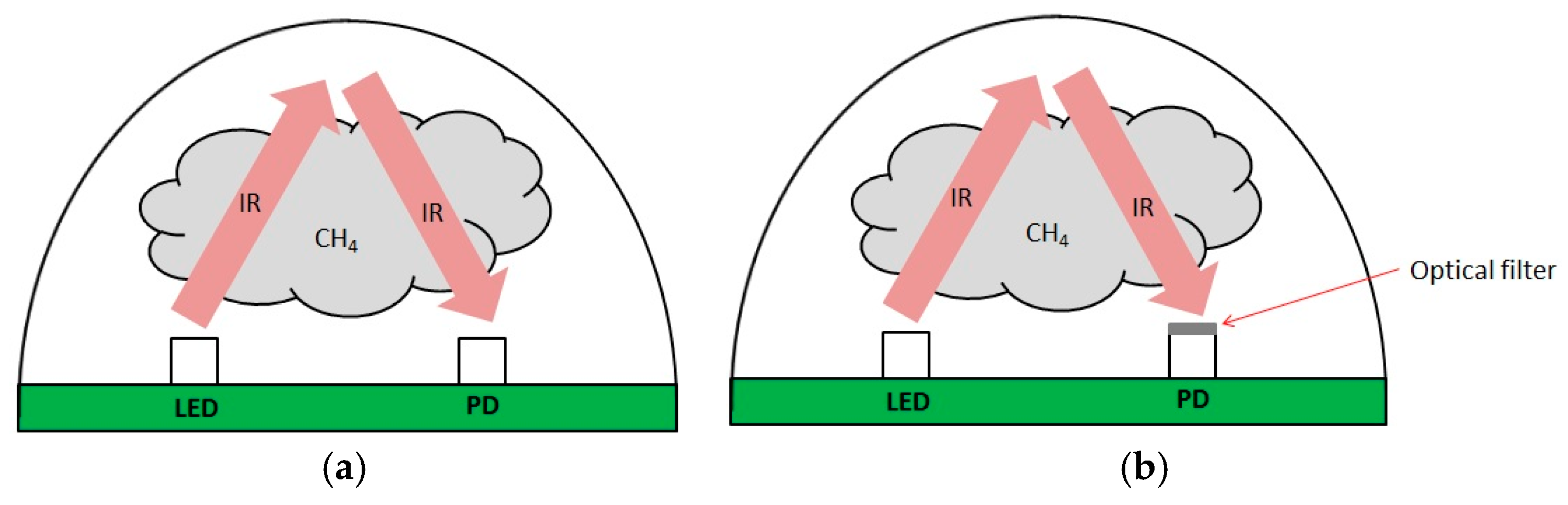
NDIR gas sensors comprise an infrared light source, optical BPF and a detector. The light source emits infrared light at a wavelength that is tuned to the infrared (IR) absorption of gas in the optical path between the source and detector. This results in a reduced IR intensity incident on the photodetector. Typically, optical BPFs are incorporated to improve the NDIR gas selectivity by narrowing the total bandwidth (BW) of the spectral response of the source-detector system, and thereby preventing cross-sensitivity with other gases and water vapour. One such solution to the problem of gas selectivity would be to use tunable semiconductor diode lasers; however, such a solution is not favourable due to high cost.
By measuring the incident light intensity
I0 and the transmitted light intensity
I of the IR light, the concentration of methane gas concentration can be calculated according to the Beer–Lambert law [
16]. A state-of-the-art NDIR CH
4 gas sensor has been utilised for this work, utilising a molecular beam epitaxy-grown pentanary alloy light-emitting diode (LED) light source and a photodiode (PD) detector, which is shown in
Figure 1a. For this work, the stoichiometry of the semiconductor source-detector pair is tuned for the maximum spectral response at 3.3 μm, coinciding with a principle absorption band of the CH
4 molecule, due to the asymmetric stretch vibrational mode [
17].
This work describes direct deposition of BPFs directly onto the LED/PD optopair, thereby optimising the spectral response shape. A room temperature deposition method that is suited to direct deposition onto the temperature-sensitive LED/PD optopair is described, and associated with the optical BPF environmental (temperature and humidity) performance. Two different optical BPF BWs were progressed to assess the effect of the filter BW on the sensor accuracy and the cross-talk reduction capability with the ultimate goal of determining whether a BW is (if any) more suited to sensor commercial production.
2. Relevant Background Work and Non-Dispersive Infrared Sensor Configuration
Work was previously carried out by Fleming et al [
18], relating to the deposition of 300 nm BW bandpass filters onto commercially available LEDs and photodiodes. This previous work was related to carbon dioxide (CO
2) detection for breath monitoring (capnography) during surgical anaesthesia [
19]. It was found that the application of the coating onto the photodiode only (as opposed to coating the LED only or both the LED and PD) with the bandpass filter design was the optimum method to isolate the CO
2 absorption band, and to reduce the cross-talk effect from the commonly used surgical anaesthetic gas, nitrous oxide (N
2O) [
20,
21].
The light emitted from the mid infrared LED is reflected from a gold-coated injection-moulded plastic dome geometry optic onto the PD. A CH4 mid infrared absorption band at 3.3 μm coincides with a CH4 anti-symmetric stretch vibrational mode. Another band exists in the long-wave infrared (LWIR), and it peaks at 7.6 μm. According to the HITRAN database, the absorption intensity of methane gas is the largest at a wavelength of 3.3 μm, and as such, this band was chosen for CH4 detection in this work.
For this reason, a bandpass BW of 300 nm was chosen for this work, and we build upon the previous work by comparing the effect of a narrower BW (160 nm) bandpass filter. A BW of 300 nm was originally chosen as this matches the BW of the 3.3 μm CH
4 absorption band. The optical coating designs were built into a comprehensive NDIR gas sensor Mathcad model, and their effects on the sensor signal accuracy and reduced cross sensitivity were determined, specifically the adjacent water absorption band at 2.8 μm. A gas sensor model predicting the measured sensor signal as a function of gas concentration was established using Mathcad [
22]. The model includes the temperature-dependent LED spectral emission and PD spectral detectivity by using a generalised form of the Planck equation [
23,
24]. The gas species’ spectral absorption characteristics were imported from the HITRAN database, and they were used to model the effect on the sensor signal as a function of gas concentration, comprising various gas mixtures in the sensor light source/detector optical path length using the Beer–Lambert law. The model includes the influence of Johnson–Nyquist noise, dark noise, and also quantisation noise, which is a result of the modelled data collection electronics. A theoretical description of the model is provided in
Section 3 of this paper.
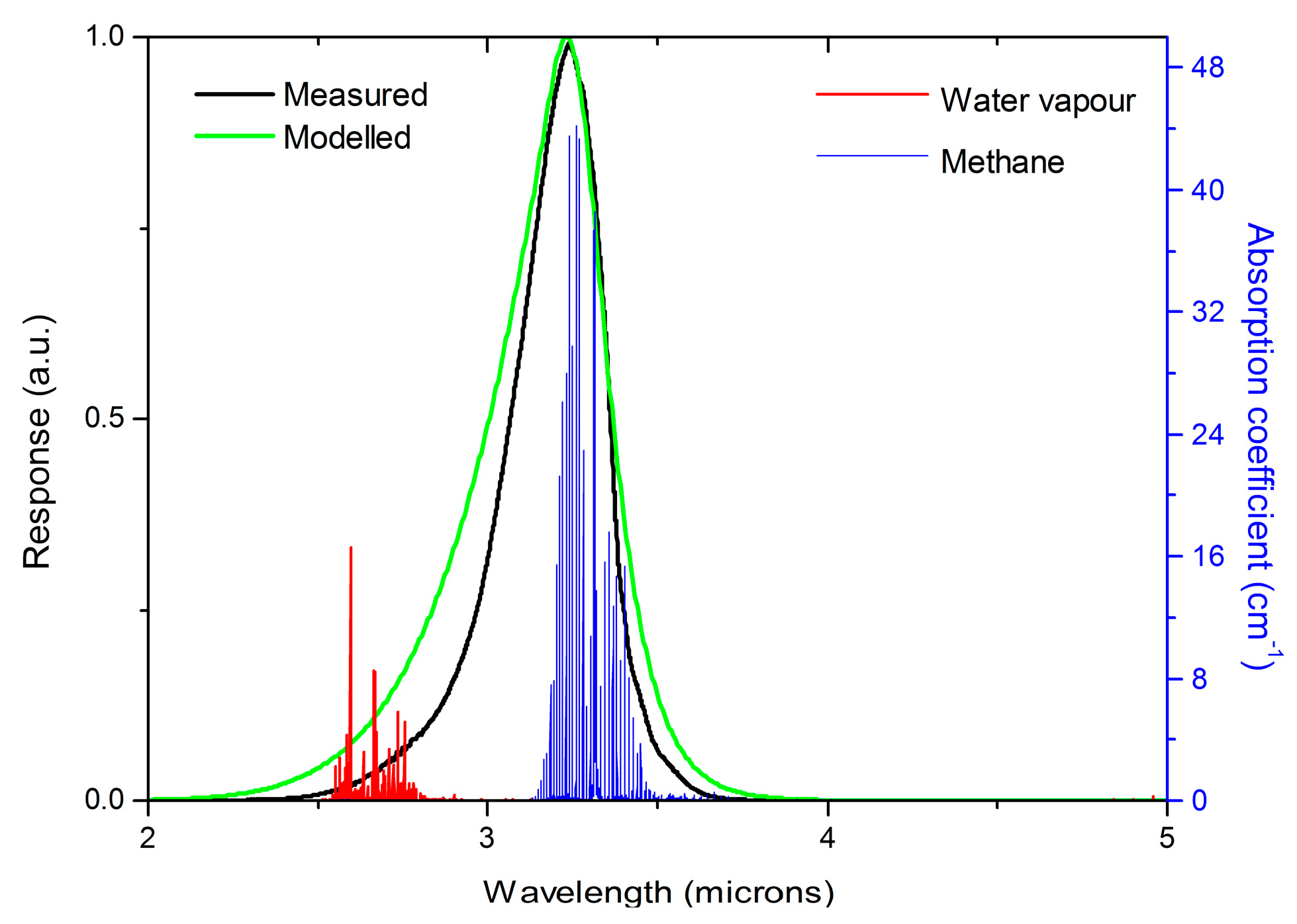
Figure 2 shows the modelled and measured spectral responses of the CH
4 sensor, indicating a good agreement between the theoretical and experimental result. Also plotted in
Figure 2 are the absorption coefficients for CH
4 and water vapour (H
2O). It can be seen that the CH
4 absorption band peak coincided with the peak of the sensor spectral response for both the modelled and experimental curves. The H
2O absorption peak lay in close proximity to the CH
4 peak, and as a result, it lay within the spectral response of the CH
4 sensor, suggesting that the sensor will suffer from cross-talk (i.e., unwanted signal contribution) from H
2O if it is present in any significant concentration. When the sensor chamber contains water vapour, this can cause significant inaccuracies in the detected CH
4 concentration. Therefore, it is advantageous to use optical filtering to reduce the influence of other gases and to improve the selectivity of the detection system. In addition, different bandpass filter designs can provide a method to influence the NDIR gas sensor detection accuracy and sensitivity. The primary purpose of this paper is to design the technical parameters of the bandpass filter according to the demand of the NDIR gas sensor, and to demonstrate room temperature direct deposition onto the LED/PD optopair, removing the need for the inclusion of a separate discrete bandpass filter.
3. Theoretical Background
3.1. Determination of Bandpass Filter Parameters
When a gas with optical transmittance
Tg is present within the gas sensor, the gas sensor total spectral response is given by:
where
S(
λ) and
D(
λ) are the respective spectral responses of the source and detector, and
Tg follows the well-known Beer–Lambert law:
where
α(
λ) is the absorption coefficient of the gas,
c is the concentration, and
l is the pathlength that the light travels through. Analogously, the total spectral response of the source-detector system can be modified by using an optical interference filter with optical transmittance
Tf. The new total spectral response for a filtered sensor
Gf becomes:
To maintain the maximised NDIR sensor sensitivity to the target gas, the Tf must have a maximum optical transmittance over the gas-absorbing spectral region, and necessary blocking of unwanted signal contributions from other gases and water vapour. Tf must be as close to zero as possible over the absorbing regions of such gases. In this work, an optical bandpass filter spectral characteristic mathematical function was modelled by using Mathcad 15, and incorporated into a comprehensive gas sensor model. The LED source emission was approximated using the generalised Planck equation, and the photodiode detectivity was modelled using the characteristic equations for a photodiode response. From this, the modelled NDIR gas sensor signal response incorporating a bandpass filter was modelled. The multilayer bandpass filter structure was modelled using thin film optical design software TFCalc (version 3.5b12), where the multilayer optical filter structure was designed such that the modelled optical transmittance matched that of the bandpass filter spectral characteristic function modelled in the Mathcad NDIR gas sensor program.
From the TFCalc [
25] model, the exact layer thicknesses and number of layers for each coating design were used as the basis for the experimental deposition of the multilayer bandpass filters. Each filter design comprises a three-cavity Fabry–Perot starting design, which were optimised by using the Variable Metric method for a maximal optical transmittance at a 3300 nm bandwidth, and out-of-band blocking. The influence of a 2.67 μm infrared absorption peak of water vapour, angle offset, and signal-to-noise ratio were taken into account during the filter design stage. Two different bandpass filters (
Table 1) were designed based on sensor signal modelling results (
Table 2) for maintaining good sensor accuracy up to the CH
4 LEL, and good blocking of H
2O absorbing wavelengths that are a considerable cause of cross-talk for this sensor design. The sensor accuracy to methane was calculated based on the slope of the calculated signal vs the concentration curve. Incorporating BPFs to the sensors’ architecture had the effect of increasing the slope and therefore sensor accuracy to methane, as well as the additional benefit of reducing signal contributions from water vapour. The results showed that the accuracy of 300 nm was lower than the accuracy of 160 nm, but was still highly adequate.
3.2. Thin Film Optical Design of the 300 nm and 160 nm BW Optical BPFs
A three-cavity Fabry-Perot BP was modelled in TFCalc, as a starting design for both the 300 nm and 160 nm BW bandpass filters. Next, a computational optimisation technique was used to alter the multilayer design in order to achieve two different bandpass filter designs, one with a 300 nm and one with a 160 nm BW passband, both with good out-of-band blocking to reduce the signal contributions from other gases.
Measured spectral transmittance is shown in
Figure 3 (note no high efficiency anti-reflection coating added to substrate back face with consequent reduction in transmission due to substrate back face reflection). For the 300 nm BW bandpass filter, the structure consisted of 34 layers, and the total thickness was 10.6 μm, the peak transmittance reached 60%, while the average transmittance in the out-of-band regions, 2–3 μm and 3.6–5 μm were 0.09% and 0.32%, respectively, and the signal-to-noise ratio (SNR) of the filter was 2.4%. For the bandpass filter with a BW of 160 nm, the number of layers was 30, with a total thickness of 9.6 μm, the peak transmittance reached 58% and the average blocking area of 2–3.1 μm and 3.5–5 μm was 0.12% and 0.31%, with a SNR of 4.5%.
4. BPF Deposition Methods and Materials
4.1. Multilayer Thin Film Optical Interference Filter Preparation Method
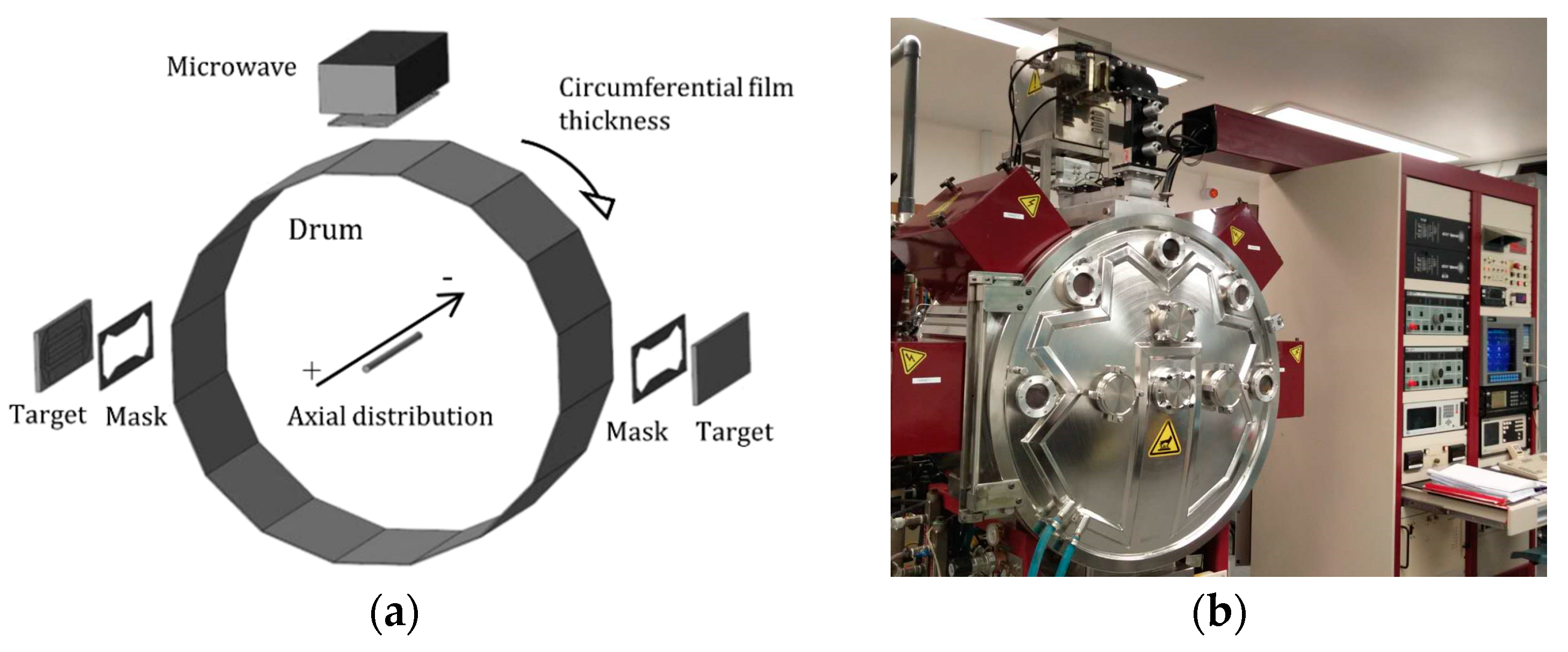
In this work, thin film optical coatings were prepared using a novel microwave plasma-assisted pulsed reactive DC magnetron technique. The system used is shown in
Figure 4. The apparatus was equipped with a complete microwave generator system comprising a 6 kW microwave magnetron head, tuner, and microwave delivery tubes. The reactive plasma ion density was greatly enhanced via the use of this external microwave source, which resulted in a greater reactive gas reactivity, and generated a greater number of monoatomic ions, resulting in a greater coating homogeneity, and reduced optical absorption in the deposited coatings. The use of pulsed DC power greatly reduces the problem of arcing caused by target poisoning and positive charge build up on the sputtering target surface, and aids in achieving a higher film deposition rate. In this work, thin films of germanium (Ge) and niobium pentoxide (Nb
2O
5) were obtained by sputtering from Ge and niobium (Nb) bulk sputtering targets, each with 99.999% (5 N) purity.
The deposition rate and thickness of the film were monitored in real-time by quartz crystal thin film thickness monitors (Inficon IC5, Inficon Inc., Bad Ragaz, Switzerland) [
26], utilising three crystals per magnetron. Argon is used as a sputter process gas, and oxygen as a reactive gas. At the same time, the pressure and flow rate of gas was accurately controlled by an optical gas controller (OGC, MKS Instruments Inc., Andover, MA, USA) and MKS mass flow controllers (MKS Instruments Inc., Andover, MA, USA), controlled by a multi-gas controller (MKS Instruments Inc., Andover, MA, USA). The chamber body was heated by hot water to liberate any residual H
2O molecules trapped on the chamber walls, and into the molecular flow regime, thereby increasing their probability of becoming trapped by Meisner cooling coils in the vacuum chamber (Telemark polycold model 3600, Telemark Inc, Battleground, WA, USA).
The removal of water vapour is essential for the growth of high quality mid-infrared optical coatings, where film density and water content play a significant role in determining the films optical absorption and spectral stability. A typical system ultimate vacuum is 5 × 10⁻⁷ mbar, minimising the adverse influence of water vapour on the optical BPF performance of the film. By adjusting the deposition process parameters, the required quality and the low absorption, Ge and Nb2O5 single layer films were deposited for optical characterisation, which are essential for the design and manufacture of multilayer thin film optical BPFs.
Specific process parameters used are shown in
Table 3. This system was used to deposit two different BPFs—specifically 300 nm BW and 160 nm BW, directly deposited onto Gas Sensing Solutions (GSS) Ltd NDIR gas sensor photodiodes for the comparison of their influence on gas sensor performance. Also included in each coating run was a 100 mm (4″) undoped <100> Czochralski grown silicon (Si) wafer and gallium arsenide (GaAs) witness pieces.
4.2. Optical Characterisation
Optical transmittance in the mid-IR range for single and multilayer coatings were obtained using a Nicolet iS-50 Fourier Transform Infrared (FTIR) spectrometer (Thermo Fischer Scientific Nicolet, Waltham, MA, USA). The optical constants, which are essential for multilayer thin film optical filter design (refractive index and absorption coefficient), were derived from the optical transmittance spectra by using a combination of the O’Leary, Johnson and Lim (OJL) model [
27] for amorphous materials, and the Drude model. The TFCalc thin film design software was then used to design a bandpass filter that met the required specifications, and to calculate the deviation between the design and the experimental results. Gas sensor photodiode spectral photocurrent responses for uncoated and coated diodes was measured using a VERTEX 80/80v FTIR (Bruker, Billerica, MA, USA), configured such that the IR beam was incident on the photodiode during testing.
4.3. Gas Sensor Testing
Calibrated gas sensors were placed in a testing chamber at room temperature and exposed to a gas mixture of N2 (which is IR-inactive and so does not elicit a response in the sensor) and CH4. The CH4 concentration was controlled by varying the continuous flow rate ratio provided by a CH4 mass flow controller (MFC, MKS Instruments Inc, Andover, MA, USA) and an N2 MFC (MFC, MKS Instruments Inc., Andover, MA, USA). A range of 0–50,000 ppm CH4 was used, and 50,000 ppm was chosen as the LEL for CH4.
5. Results & Discussion
5.1. Thin Film Optical Constant Derivation
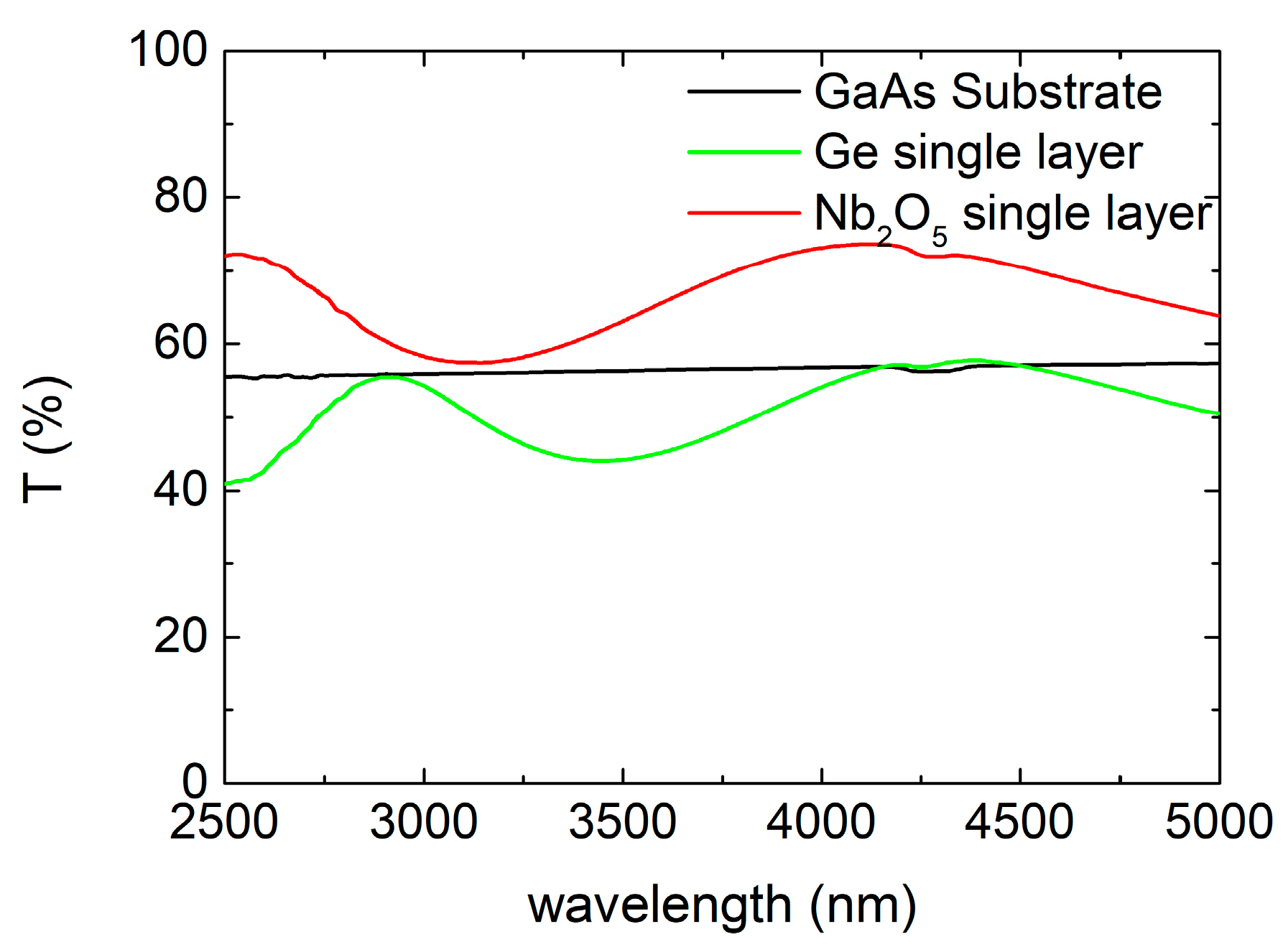
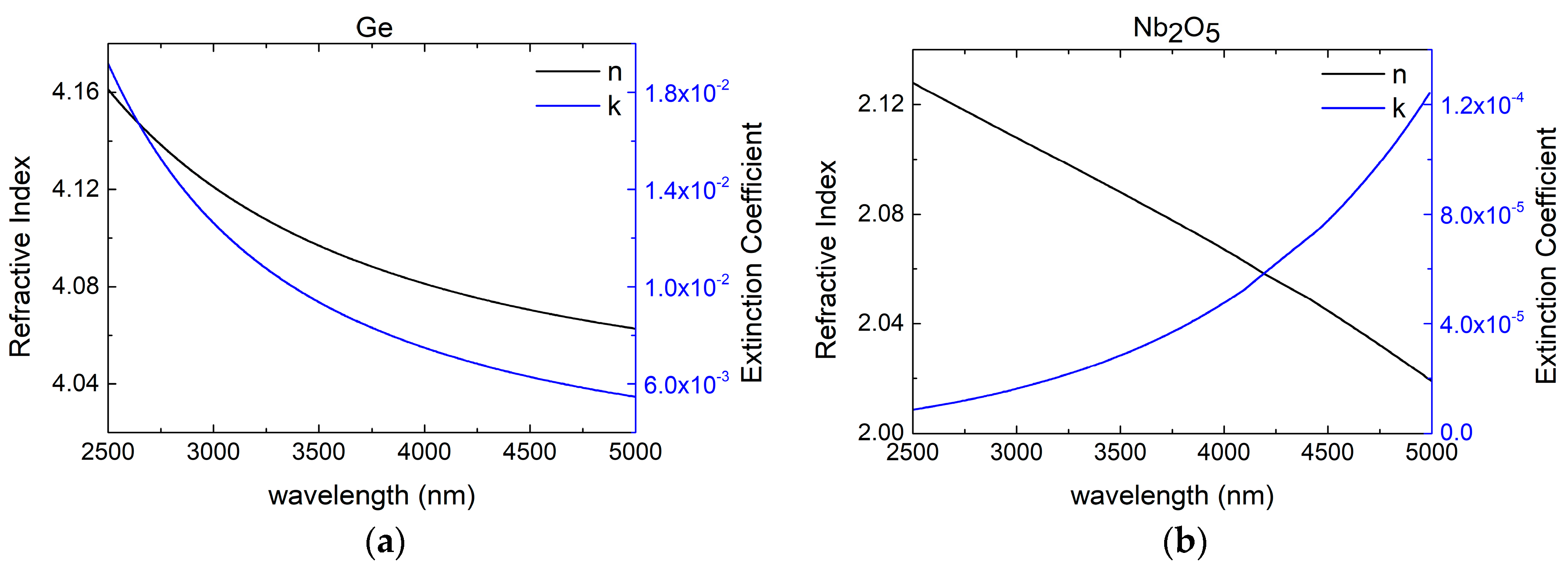
Single layers were deposited onto a 500 μm thick gallium arsenide (GaAs) substrate. The optical transmittance spectra for a single layer of 1 μm Ge and 1.5 μm Nb
2O
5 as measured using FTIR is shown in
Figure 5, and overlaid with the uncoated GaAs substrate spectrum for comparison. The calculated optical constants are shown in
Figure 6. It can be seen that the absorption coefficient of the thin film materials are minimal, with refractive index contrast between the Ge and Nb
2O
5 thin films was large, suggesting that these materials are acceptable material candidates for use in the fabrication of mid-infrared multilayer optical BPFs.
5.2. Multilayer Thin Film Optical Interference Bandpass Filter Deposition
Two different bandpass filter Ge/Nb
2O
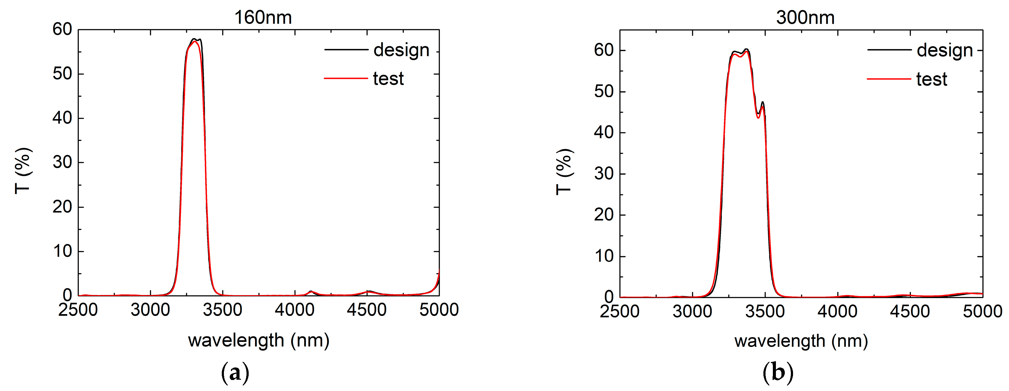
5 multilayer designs were deposited onto GSS methane sensor photodiodes using precision laser cut masking, thereby masking the rest of the bridgeboard LED structure. The spectral transmittance characteristic curve of each bandpass filter was obtained using the Nicolet iS-50 FTIR on the witness samples present during the coating runs.
Figure 7 shows excellent agreement between the theoretical design and the measured results of the two optical BPFs (note no high efficiency anti-reflection coating added to substrate back face with consequent reduction in transmission due to substrate back face reflection). It can be seen that the actual transmittance of the 160 nm and 300 nm BPFs were 57% and 58% respectively, which was in excellent agreement with the design values. This is because the deposited thickness was greater than the model, resulting in a slightly higher optical absorption. However, this slight mismatch between theory and design was negligible, as the bandpass centre wavelength (CWL) at 3300 nm and BW remained the same—the two critical parameters for maintaining gas sensor sensitivity to CH
4 and for out-of-band blocking of the H
2O infrared absorption band were centred at 2.67 μm. Bandpass filter design parameters for 160 nm BW and 300 nm BW are shown in
Table 1.
5.3. Uncoated and Coated Gas Sensor Photodiode Photocurrent Spectral Responses
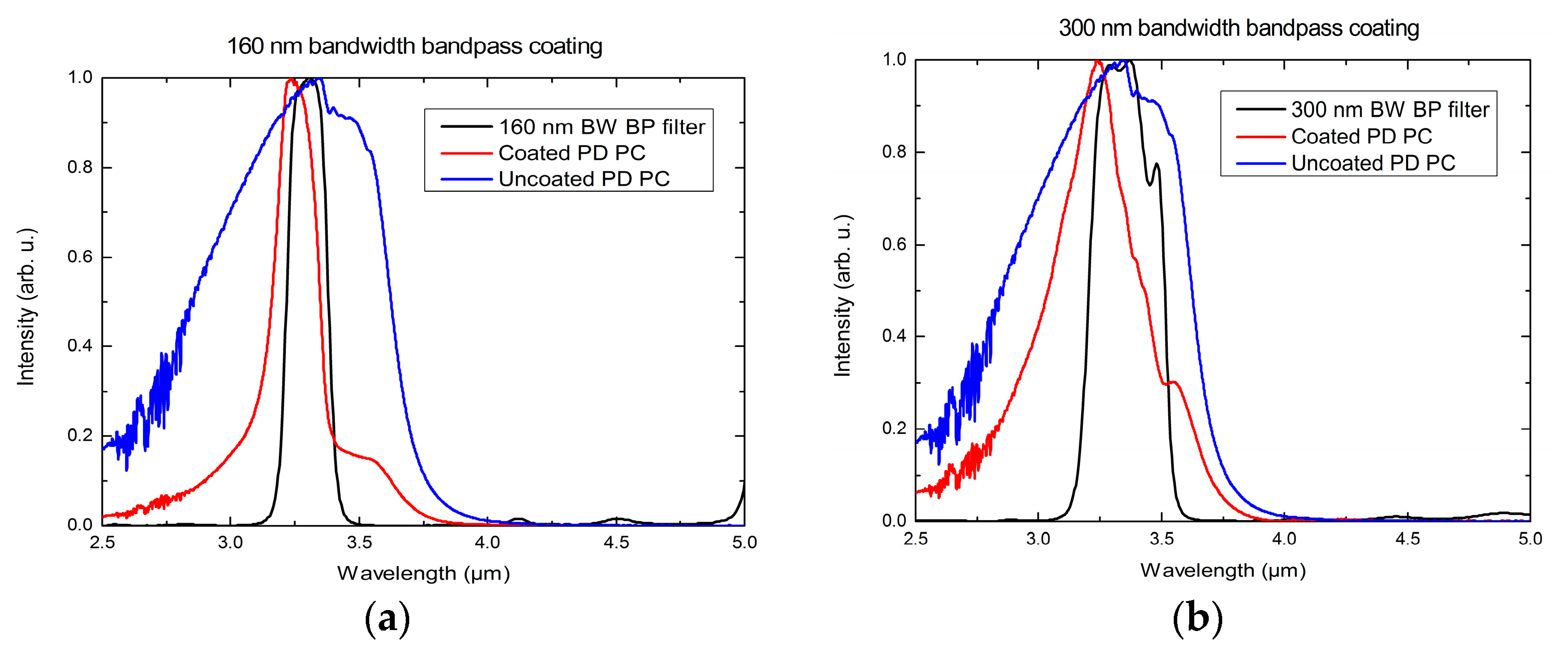
The aforementioned coatings were applied to the GSS CH
4 gas sensor LED/PD bridgeboards tuned for emission and detection at the CH
4 absorption wavelength at 3.3 μm. The LED/PD bridgeboard was masked apart from the PDs, enabling the optical coating to be applied to the photodiode. Using a Bruker VERTEX 80/80v FTIR, the spectral response of the uncoated and coated diode heterostructure was recorded.
Figure 8 shows the BPF influence on the photodiode photocurrent response when illuminated with broadband IR radiation.
It can be seen that the coated photodiode photocurrent (PC) response was shaped by the optical filter spectral transmittance characteristic. Whilst the response at the 2800 nm water vapour absorption band was not entirely eliminated, application of the optical BPF provides a significant reduction in the photodiode BW photocurrent response. Therefore the total sensor spectral response is reduced, lowering the response at wavelengths outside the CH4 absorption band and minimising sensor responses to gases other than CH4 and also improving the accuracy of the sensor for the CH4 target gas.
The backface of the photodiode was unpolished, therefore, it is suspected that the unpolished surface result in incident light at wavelengths to be scattered at higher angles for which the bandpass filter was not designed. This results in signal contributions from the H2O band, with a slight detrimental effect on the selectivity of the sensor. Here it was demonstrated that different optical filter designs can be readily applied to the sensor photodiode, allowing for a greater flexibility in sensor design and the ability to customise and optimise NDIR gas sensor design to specific customer applications.
5.4. Gas Sensor Testing Results
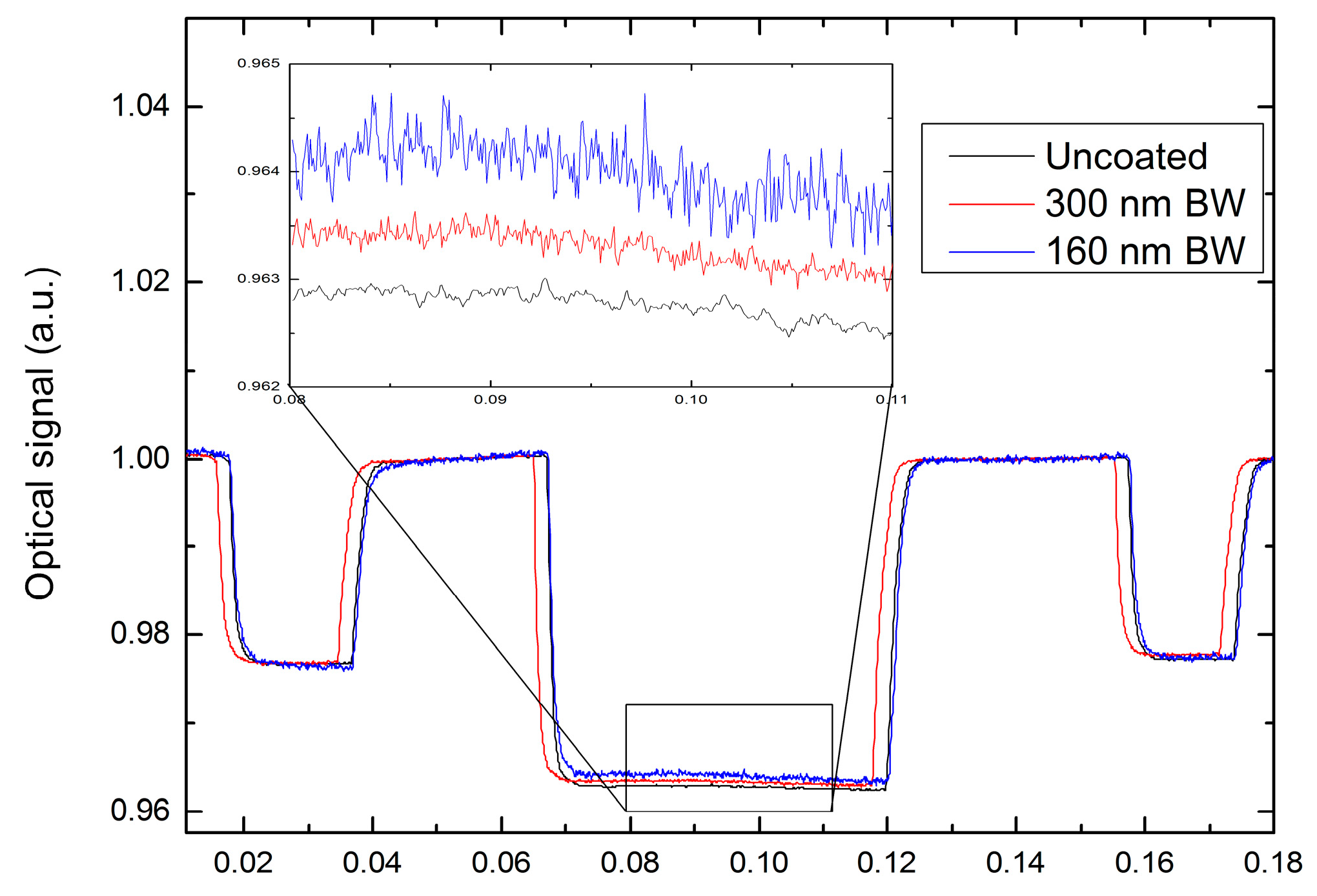
The signal as a function of time for a 160 nm BW BP and a 300 nm BW BP-coated sensor is shown in
Figure 9. The sensors were calibrated for temperature compensation, and then exposed to a nitrogen (N
2)/CH
4 gas mixture, where the CH
4 concentration was cycled between 0%, 2.5%, and 5% CH
4 concentration over a duration of 4 h. From
Figure 9, it can be seen that both the 160 and 300 nm BW BP-coated sensors showed a similar response to this variation in CH
4 concentration. As expected, the SNR performance of the 300 nm BW BP-coated sensor was superior to the 160 nm BW BP sensor, as a result of a greater intensity of IR light that was transmitted through the BPF.
For this reason, we suggest it is suggested the 300 nm BW BP filter is a better choice than the 160 nm BW BP filter, as it has an improved SNR performance.
Table 4 shows the calculated root-mean-square (RMS) noise for 5%, 2.5%, and 0% CH
4, for both the 160 nm BW BP-coated and 300 nm BW BP-coated sensors. Generally, RMS noise increases with increasing gas concentration, as more light is absorbed, and less light is incident on the sensor photodiode. The calculated values for 2.5% and 0% methane for the 160 nm BW BP sensor did not reflect this; however, the authors suspect that this may be due to the small sample size collected for 2.5% methane.
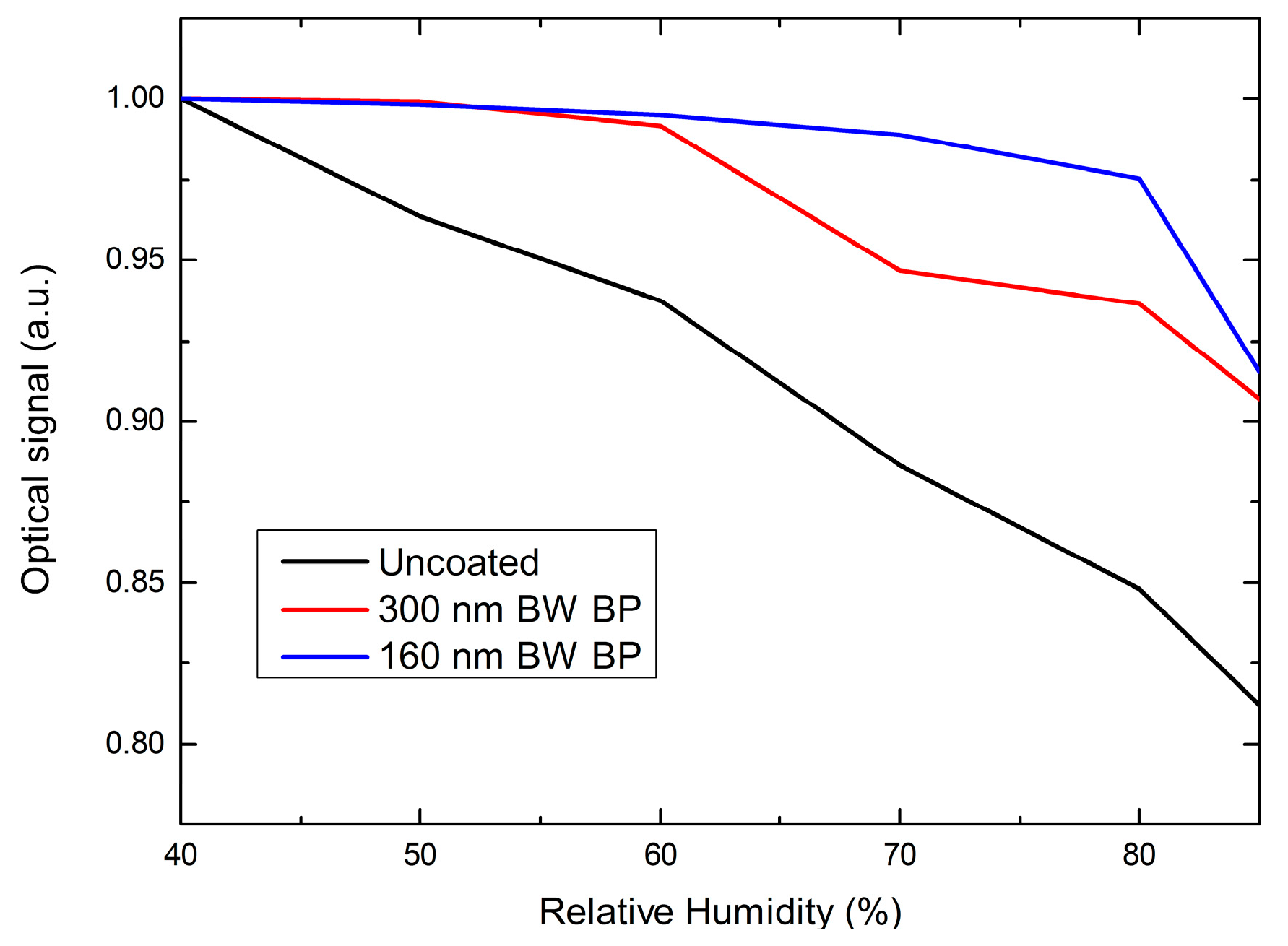
The sensors were then placed in an environmental chamber (WKL 34, Weiss Technik, Grand Rapids, MI, USA), and exposed to an increasing relative humidity (RH), testing sensor crosstalk that was attributable to increasing H
2O vapour concentration. Water vapour concentration in the chamber was proportional to relative humidity. It can be seen from
Figure 10 that the optical signal for an uncoated sensor dropped the fastest with increasing RH, as compared with the 300 nm and 160 nm BW BP-coated sensors. This suggests that the uncoated sensor was the most sensitive to H
2O vapour. The 160 and 300 nm BW BP-coated sensors displayed a similar performance of up to 60% RH, with the 160 nm sensor demonstrating less sensitivity to H
2O vapour. Optical signal levels also exhibited increased changes for RH > 80%. This was ascribed to condensation occurring on the sensor optics.
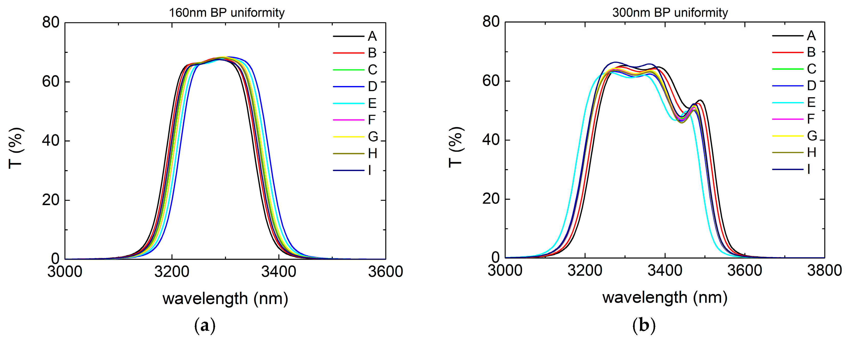
5.5. Wafer Uniformity Test
Work has previously been carried out by Cheng et al. [
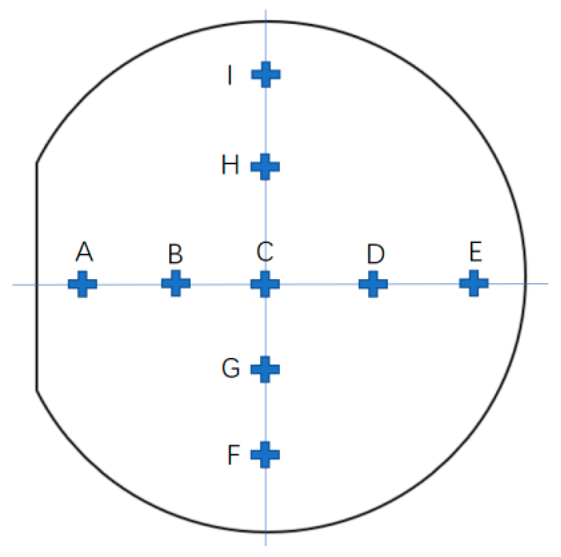
28], evaluating the coating thickness uniformity using the microwave plasma-assisted sputtering technique used in this work. In this work, the LED/PD bridgeboards were mounted onto specially designed toolings with precision masking, permitting application of the BPF coating to the photodiode surface area only, however, this method may not be optimal for scalable mass production of coated photodiodes. A more optimal method would be to sputter-deposit the coating onto an enitre photodiode wafer directly after it has been grown by molecular beam epitaxy (MBE) prior to dicing and mounting onto the sensor bridgeboards. For this reason, both the 160 nm and the 300 nm BW bandpass filter optical coating designs were each successfully deposited onto 100 mm diameter (4″) <100> undoped silicon (Si) wafers with 500 μm thickness, grown by the Czochralski method and tested for coating uniformity. This demonstrates that the bandpass filter spectral characteristic was uniform over an entire 4″ wafer and suitable for coating an entire newly grown photodiode wafer.
The Si wafer was mounted onto the deposition system’s rotating drum, such that the wafer flat was parallel with the circumference of the drum, as depicted in
Figure 11. Post-coating, the wafer was then diced into 20 mm × 20 mm squares and each section’s position was labelled and measured using FTIR to compare the spectral variation in their optical transmittances. The results for the 160 nm and 300 nm BW bandpass filters are plotted in
Figure 12.
From these spectra, the coating uniformity was calcaulted for both the 300 nm badwidth bandpass filter and the 160 nm BW bandpass filter, and the results are shown in
Table 5.
These small deviations show that excellent coating thickness uniformity can be achieved across an entire 100 mm diameter wafer, maintaining the desired optical transmittance spectral characteristics by preserving optical transmittance over the CH4 absorption band, and improving blocking at H2O absorption wavelengths. This indicates that coating an entire photodiode wafer prior to dicing and mounting onto electronics bridgeboards, is a potential production-efficient way of incorporating optical filters into NDIR gas sensor. From modelling, it was found that increasing every layer by the same factor, a change in peak spectral position of 344 nm per micron of total coating thickness would be observed —this provides an indication on coating tolerance.
5.6. Accelerated Lifetime Testing
A common accelerated lifetime test to probe the optical and structural integrity of thin film coatings is provided by subjecting the samples to a pressure cooker test, where coated witness samples are subjected to a prolonged exposure to high temperature sper-saturated steam and high pressure by using a pressure cooker (pressure 15 psi). The pressure cooker test is a good indicator of coating durability in harsh environments. The center pieces from coated 100 mm diameter Si wafers for both the 160 nm BW bandpass and the 300 nm BW bandpass were placed into the center of a pressure cooker with a maximum pressure of 15 psi. The samples were subjected to pressure cooker exposure times of 5, 10, 20 and 40 min, with optical transmittances measured by FTIR in between each step.
From
Figure 13 it can be seen that the optical filter spectral characteristics remained largely the same for all time durations, where a small reduction in peak transmittance was observed for the 160 nm BW bandpass filter. For the 300 nm BW bandpass filter the only minimal change in peak optical transmittance occurred at 5, 10 and 20 min; however, the drop in transmittance was more pronouned at 40 min. Differences between the 160 nm BW and the 300 nm BW bandpass samples are most likely to be attributable to the top layer being different, as for 160 nm, the top layer was Ge and for 300 nm it was Nb
2O
5.
The diode surface that the coatings were applied to was the unpolished underside of GaAs, therefore factors such as high substrate surface roughness may also be a contributing factor in determining the coating’s mechanical integrity for actual gas application sensing; however, coatings applied to the gas sensor photodiode element were not be subjested to such a harsh environment, and so it can be safely assumed that the disruption of the coating’s optical properties is unlikely to occur.
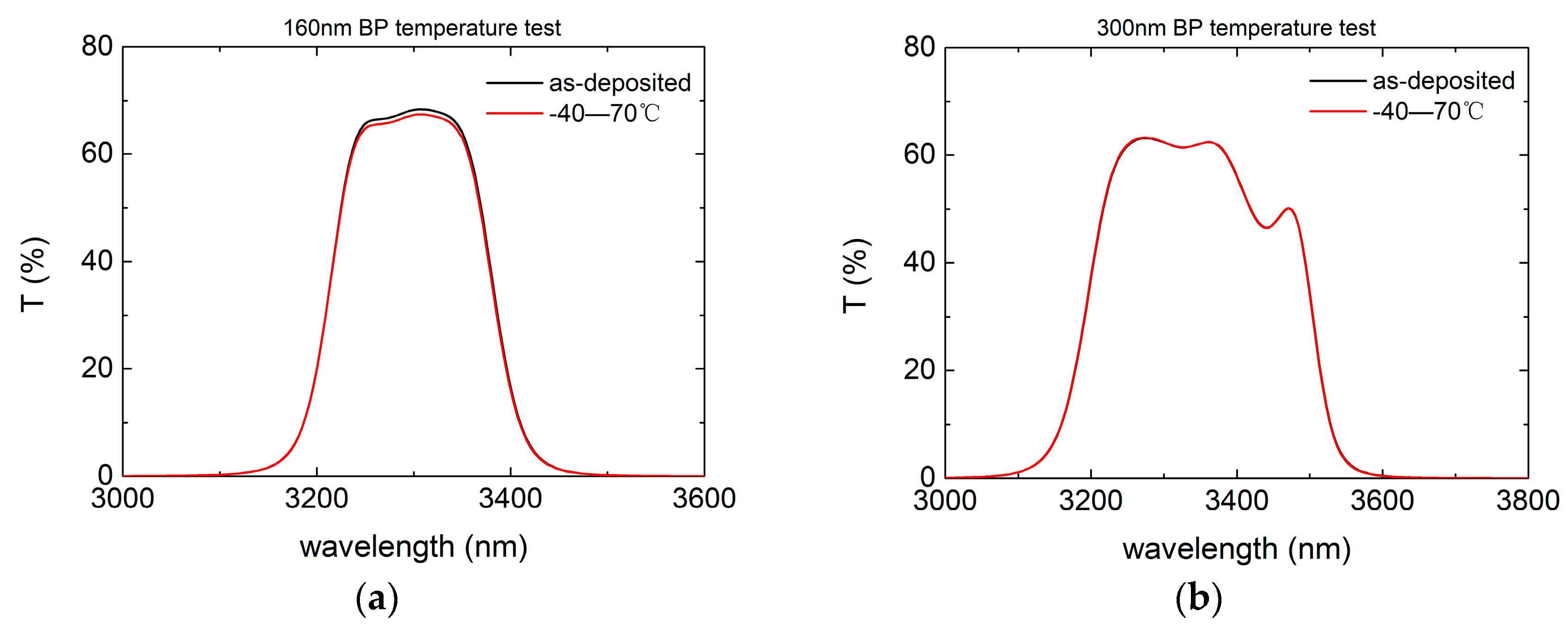
5.7. Humidity and Temperature Testing
Gas sensors in different temperature and humidity environments will have different performance parameters, and so it is necessary to perform humidity and temperature tests for the optical filter. The closed central pieces of the coated Si wafer for both the 160 nm BW bandpass and the 300 nm BW bandpass were placed into the WKL Temperature and Climatic Test System. The humidity test was carried out at 50 °C and 95% humidity for 24 h (
Figure 14), and the temperature test was −40 to 70 °C (
Figure 15), where the temperature was increased by 10 °C every two hours.
6. Conclusions
In this work, the spectral response of a methane sensor comprising a heterostructure LED/PD optopair was modelled and compared with the experimentally measured spectral response, with good agreement. The accuracy of such an NDIR gas sensor was modelled from the design spectral response. Single layers of Nb2O5 and Ge were deposited onto optical substrates, and optically characterised to obtain their refractive indices and extinction coefficients, subsequently used in the design of two multilayer optical interference BP filters; with passbands with BW’s of 300 nm and 160 nm. These designs were then sputter-deposited onto MBE-grown heterostructural diodes with the peak detectivity tuned to 3300 nm (coinciding with the CH4 absorption band to be used in the interest of CH4 gas detection) using microwave plasma-assisted pulsed DC magnetron sputtering.
The thin film multilayer filters were also deposited onto full 4″ Si wafers in the same coating run. The coated and uncoated PD PC responses were measured using an FTIR spectrophotometer, and it was demonstrated that the PD PC spectral response conformed to the spectral shape of the applied optical filter for both 300 and 160 nm BW BP filters. These coated PDs were then built into gas sensor electronics with full injection moulded plastic optics, and tested under various CH4 gas concentrations for comparison. The gas concentration was cycled from 0%, 2.5%, and 5% CH4 concentrations, to test the sensor’s capability for measuring concentrations of CH4 below the LEL. As expected, it was observed that the 160 nm BW BP-coated sensor displayed more noise as compared to the 300 nm BW BP sensor, due to the reduced intensity of the IR incident of the PD, and therefore a poorer SNR. The 160 nm BW BP-coated sensor, having a narrower BW as compared with the 300 nm BW BP-coated sensor, will be less susceptible to cross-talk-inducing gases, given this cross-talk/noise level trade-off. Noise levels could be electronically filtered out at the expense of lowering the measurement frequency of the sensor, and therefore the different BW optical filter coatings designs may be suited better to different applications with different measurement frequencies and accuracy requirements. The sensors were then tested in an environmental humidity chamber and exposed to increasing humidity levels and therefore water vapour vapour concentration. It was found that the uncoated sensor was most sensitive to water vapour, followed by 300 nm BW BP-coated sensors then the 160 nm BW BP-coated sensor which was found to be least sensitive.
In addition to the testing improvement of gas sensor performance by using multilayered optical coatings, coating uniformity and structural integrity tests under various environmental conditions were carried out. As described, the multilayer filters were deposited onto full 4″ Si wafers. The wafers were then diced, and the optical transmittance of each section was measured, showing excellent thickness uniformities over a 100 mm diameter of ±0.355% and ±0.530% for 160 and 300 nm BW BP coatings, respectively. This demonstrates that full-production wafers can be successfully coated and subsequently diced without disruption to the optical coating, indicating that full PD production wafers can also be coated prior to dicing.
Witness samples (Si substrates) coated with the multilayer thin film optical filter were then subjected to accelerated lifetime testing by using a pressure cooker to expose the coating to high heat and high pressure for different lengths of time. The optical transmittance was measured after 5, 10, 20, and 40 min to observe the effect on the optical properties of the coating. It was found that no significant shift occurred up to 40 min; however, a slight change in peak transmittance was observed and hypothesised to be due to the absorption of H2O into the film matrix, or potential particulate contamination from the water used in the test; however, an exact mechanism for the cause will be a future investigation. Such a reduction in optical transmittance would slightly reduce the SNR and have a minimal effect on the sensor selectivity, where it is the bandpass spectral position that is the dominating factor on selectivity, with peak optical transmittance being of secondary importance.
The witness samples were also subjected to less severe but longer duration temperatures and humidity testing in an environmental chamber. The samples were subjected to a humidity test, where they were exposed to 50 °C and 95% RH for 24 h, after which the optical transmittance was measured. The temperature test comprised of exposing the coating to a temperature range of −40 to 70 °C, where the temperature was held for 2 h at each temperature and ramped up by 10 °C every 2 h—after this test, the optical transmittance was also measured. For both the temperature and humidity tests, no significant change in the optical transmittance of the samples was observed, suggesting that the deposited films were highly dense and are unlikely to undergo delamination in conditions in which the CH4 gas sensor would be present. In future work, a full suite of testing such as adhesion, hardness, and stress measurements on such coatings will be performed.
Author Contributions
Conceptualisation, D.G. and C.M.; Methodology, D.G. and X.F.; Software, S.S., M.M. and L.F.; Validation, D.G. and X.F.; Formal Analysis, L.F. and S.S.; Investigation, S.A., S.S., X.F., D.G., L.F. and P.W.; Resources, S.S. and D.G.; Data Curation, M.S., D.M., and S.S.; Writing—Original Draft Preparation, L.F., D.G., and C.L.; Writing—Review and Editing, L.F. and D.G.; Supervision, D.G, and D.H.
Funding
This research received funding from ERANET Horizon 2020 PhotonicSensing Transnational project (File Ref: 620130, ERA-NET Ref: CSMIS) and Scottish Enterprise High Growth Start-Up Project (Ref PS7305CA43). This work was also supported in part by a joint funded grant from Scottish Enterprise and CENSIS under the MIRAGE programme. The work was also funded from a University of the West of Scotland masters project.
Acknowledgments
The authors acknowledge technician support from Andy Bunyan. Also provision of mid infrared light emitting diode and photodiode bridgeboards from Gas Sensing Solutions Ltd.
Conflicts of Interest
The authors declare no conflict of interest.
References
- Mitchell, J.F.B. The “Greenhouse” effect and climate change. Rev. Geophys. 1989, 27, 115–139. [Google Scholar] [CrossRef]
- Zhang, T.; Nix, M.B.; Yoo, B.Y.; Deshusses, M.A.; Myung, N.V. Electrochemically functionalized single-walled carbon nanotube gas sensor. Electroanalysis 2006, 18, 1153–1158. [Google Scholar] [CrossRef]
- Christensen, T.H.; Cossu, R.; Stegmann, R. Environmental aspects. In Landfilling of Waste: Biogas, 1st ed.; Taylor & Francis: Oxford, UK, 1996; pp. 258–260. [Google Scholar]
- Tchobanoglous, G.; Theisen, H.; Vigil, S.A.; Alaniz, V.M. Introduction. In Integrated Solid Waste Management: Engineering Principles and Management Issues; King, P.H., Eliassen, R., Eds.; McGraw-Hill International Editions: New York, NY, USA, 1993; pp. 1–13. [Google Scholar]
- Yaws, C.L.; Braker, W. Matheson Gas Data Book; McGraw-Hill Professional: New York, NY, USA, 2001. [Google Scholar]
- Britton, L.G. Using material data in static hazard assessment. Process Saf. Prog. 1992, 11, 56–70. [Google Scholar] [CrossRef]
- Dreisbach, F.; Staudt, R.; Keller, J.U. High pressure adsorption data of methane, nitrogen, carbon dioxide and their binary and ternary mixtures on activated carbon. Adsorption 1999, 5, 215–227. [Google Scholar] [CrossRef]
- Tadesse, K.; Smith, A.; Brydon, W.G.; Eastwood, M. Gas chormatographic technique for combined measurement of hydrogen and methane using thermal conductivity detector. J. Chromatogr. A 1979, 171, 416–418. [Google Scholar] [CrossRef]
- Lee, J.H.; Trimm, D.L. Catalytic combustion of methane. Fuel Process. Technol. 1995, 42, 339–359. [Google Scholar] [CrossRef]
- The PID Handbook—Theory and Applications of Direct-Reading Photoionization Detectors (PIDs), 3rd ed.; RAE Systems Inc.: San Jose, CA, USA; 2013.
- Zhu, Z.; Xu, Y.; Jiang, B. A one ppm NDIR methane gas sensor with single frequency filter denoising algorithm. Sensors 2012, 12, 12729–12740. [Google Scholar] [CrossRef]
- Tan, Q.; Tang, L.; Yang, M.; Xue, C.; Zhang, W.; Liu, J.; Xiong, J. Three-gas detection system with IR optical sensor based on NDIR technology. Opt. Lasers Eng. 2015, 74, 103–108. [Google Scholar] [CrossRef]
- Hodgkinson, J.; Tatam, R.P. Optical gas sensing: A review. Meas. Sci. Technol. 2012, 24, 012004. [Google Scholar] [CrossRef]
- Dinh, T.V.; Choi, I.Y.; Son, Y.S.; Kim, J.C. A review on non-dispersive infrared gas sensors: Improvement of sensor detection limit and interference correction. Sens. Actuators B Chem. 2016, 231, 529–538. [Google Scholar] [CrossRef]
- Gas Sensing Solutions. Available online: https://www.gassensing.co.uk (accessed on 2 July 2018).
- Bouguer, P. Essai d’Optique sur la Gradation de la Lumière; Claude Jombert: Paris, France, 1729; pp. 16–22. (In French) [Google Scholar]
- Rothman, L.S.; Gordon, I.E.; Barbe, A.; Benner, D.C.; Bernath, P.F.; Birk, M.; Boudon, V.; Brown, L.R.; Campargue, A.; Champion, J.-P.; et al. The HITRAN 2008 molecular spectroscopic database. J. Quant. Spectrosc. Radiat. Transf. 2009, 110, 533–572. [Google Scholar] [CrossRef]
- Fleming, L.; Gibson, D.; Song, S.; Li, C.; Reid, S. Reducing N2O induced cross-talk in a NDIR CO2 gas sensor for breath analysis using multilayer thin film optical interference coatings. Surf. Coat. Technol. 2018, 336, 9–16. [Google Scholar] [CrossRef]
- Why Capnography? Available online: http://www.capnography.com/capnography-introduction/why-capnography (accessed on 19 December 2018).
- Mipex Tech. Available online: https://mipex-tech.com (accessed on 30 July 2018).
- Fleming, L. Reducing N2O Induced Cross-Talk in a NDIR CO2 Gas Sensor Using Multilayer Thin Film Optical Interference Filters. Ph.D Thesis, The University of the West of Scotland, Paisley, UK, November 2017. [Google Scholar]
- PTC Mathcad. Available online: https://www.ptc.com/en/products/mathcad (accessed on 30 July 2018).
- Smestad, G.P. Generalized model of a solar converter. In Optoelectronics of Solar Cells; SPIE Press: Bellingham, WA, USA, 2002; pp. 55–60. [Google Scholar]
- Smestad, G.; Ries, H. Luminescence and current-voltage characteristics of solar cells and optoelectronic devices. Sol. Energy Mater. Sol. Cells 1992, 25, 51–71. [Google Scholar] [CrossRef]
- Software Spectra Inc. Available online: http://www.sspectra.com/ (accessed on 20 September 2018).
- Inficon. IC/5 Thin Film Deposition Controller Manual. Available online: https://products.inficon.com/getattachment.axd/?attaName=f23367c6-34f1-446a-814a-8327045d0c59 (accessed on 20 September 2018).
- O’Leary, S.K.; Johnson, S.R.; Lim, P.K. The relationship between the distribution of electronic states and the optical absorption spectrum of an amorphous semiconductor: An empirical analysis. J. Appl. Phys. 1997, 82, 3334–3340. [Google Scholar] [CrossRef]
- Li, C.; Song, S.; Gibson, D.; Child, D.; Waddell, E. Modeling and validation of uniform large-area optical coating deposition on a rotating drum using microwave plasma reactive sputtering. Appl. Opt. 2017, 56, C65–C70. [Google Scholar] [CrossRef] [PubMed]
Figure 1.
Schematic of the CH4 gas sensor (a) without and (b) with an optical filter.
Figure 1.
Schematic of the CH4 gas sensor (a) without and (b) with an optical filter.
Figure 2.
Modelled total sensor spectral response, semi-empirical sensor response, and CH4 and H2O absorption coefficients.
Figure 2.
Modelled total sensor spectral response, semi-empirical sensor response, and CH4 and H2O absorption coefficients.
Figure 3.
Measured spectral characteristics for the optimised 300 nm BW bandpass and 160 nm BW bandpass filter designs.
Figure 3.
Measured spectral characteristics for the optimised 300 nm BW bandpass and 160 nm BW bandpass filter designs.
Figure 4.
(a) Schematic of the microwave plasma-assisted sputter reactor used to deposit the thin optical films described in this work, and (b) the image of the actual chamber. Right- and left-hand-side magnetrons were used, populated with Ge on Nb target material.
Figure 4.
(a) Schematic of the microwave plasma-assisted sputter reactor used to deposit the thin optical films described in this work, and (b) the image of the actual chamber. Right- and left-hand-side magnetrons were used, populated with Ge on Nb target material.
Figure 5.
Optical transmittance spectra of the GaAs substrate, the Ge single layer and the Nb2O5 single layer.
Figure 5.
Optical transmittance spectra of the GaAs substrate, the Ge single layer and the Nb2O5 single layer.
Figure 6.
Optical constants for (a) thin film Ge and (b) thin film Nb2O5 as calculated by using a combination of the O’Leary, Johnson and Lim (OJL) and Drude models.
Figure 6.
Optical constants for (a) thin film Ge and (b) thin film Nb2O5 as calculated by using a combination of the O’Leary, Johnson and Lim (OJL) and Drude models.
Figure 7.
Comparison between theory and experiment for (a) the 160 nm BW bandpass filter and (b) the 300 nm BW bandpass filter designs.
Figure 7.
Comparison between theory and experiment for (a) the 160 nm BW bandpass filter and (b) the 300 nm BW bandpass filter designs.
Figure 8.
Overlay of coated and uncoated CH4 photodiode photocurrent response coated with (a) 160 nm BW bandpass filter and (b) 300 nm BW bandpass filter. The spectral characteristics for the measured witness samples are also shown. It can be seen that in both cases, the photodiode photocurrent response shapes conform to the shape of the optical filter spectral characteristic. The photodiode (PD) photocurrent (PC) response does not entirely conform to the shape of the optical filter, as signal contributions from light incident at a higher angle is transmitted resulting in a broader PD PC curve that is broader than the optical filter transmittance curve.
Figure 9.
Calibrated sensor signal response for uncoated, 160 nm BW bandpass (BP)-coated and 300 nm BW BP-coated sensors when cycled from 0, 25,000, and 50,000 ppm methane (LEL) over the course of 4 h. The inset plot shows an exploded view of the signal at 5% methane, highlighting the different noise characteristic between the uncoated, 300 nm BW BP-coated sensor and the 160 nm BW BP-coated sensor.
Figure 10.
Measured optical signal as a function of increasing RH for uncoated, 160 nm BW BP, and 300 nm BW BP-coated sensors. It can be seen that the uncoated sensor was the most sensitive to increasing H2O concentration, due to the sharp drop-off of the optical signal vs RH curve, therefore successfully demonstrating that by application of the narrow BPF, sensitivity to H2O vapour is reduced.
Figure 11.
Schematic of a 4″ Si wafer as mounted onto the microwave plasma-assisted sputter coater drum. Post-coating, the wafer was diced into 20 × 20 mm2 sections, and the optical transmittances were measured for samples A–I to test for coating thickness uniformity. This was assessed for both the 300 nm and 160 nm BW bandpass filters.
Figure 12.
(a) Optical transmittance spectral characteristics for different Si wafer location samples A–I for the 160 nm BW bandpass filter; (b) Optical transmittance spectral characteristics for different Si wafer location samples A–I for the 300 nm BW bandpass filter.
Figure 12.
(a) Optical transmittance spectral characteristics for different Si wafer location samples A–I for the 160 nm BW bandpass filter; (b) Optical transmittance spectral characteristics for different Si wafer location samples A–I for the 300 nm BW bandpass filter.
Figure 13.
Optical transmittances of (a) a 160 nm and (b) a 300 nm BW bandpass witness sample after being subjected to 15 psi inside a pressure cooker for varying durations.
Figure 13.
Optical transmittances of (a) a 160 nm and (b) a 300 nm BW bandpass witness sample after being subjected to 15 psi inside a pressure cooker for varying durations.
Figure 14.
Optical transmittance of (a) the 160 nm and (b) the 300 nm BW bandpass witness sample after a humidity test.
Figure 14.
Optical transmittance of (a) the 160 nm and (b) the 300 nm BW bandpass witness sample after a humidity test.
Figure 15.
Optical transmittance of (a) the 160 nm and (b) the 300 nm BW bandpass witness sample after the temperature test.
Figure 15.
Optical transmittance of (a) the 160 nm and (b) the 300 nm BW bandpass witness sample after the temperature test.
Table 1.
Comparison of technical parameters between the 160 and 300 nm bandpass filter.
Table 1.
Comparison of technical parameters between the 160 and 300 nm bandpass filter.
| Bandpass Filter Parameter | 160 nm BW Filter | 300 nm BW Filter |
|---|
| Central wavelength (μm) | 3.3 | 3.325 |
| FWHM (nm) | 160 | 300 |
| T (peak) | 73% | 85% |
| Blocking (μm) | 2–5 | 2–5 |
Table 2.
Comparison of the sensor accuracy to methane by using 160 and 300 nm band pass filters.
Table 2.
Comparison of the sensor accuracy to methane by using 160 and 300 nm band pass filters.
| CH4 Concentration Range (ppm) | 160 nm BW Filter (%) | 300 nm BW Filter (%) |
|---|
| 10–100 | 6.2 | 7.7 |
| 100–1000 | 0.6 | 0.8 |
| 1000–50000 | 0.01 | 0.02 |
Table 3.
The deposition process parameters used to grow thin films of Ge and Nb2O5. Ten kilowatt advanced energy magnetron drive (MDX) power supplies were used in voltage regulation and current regulation mode for Ge and Nb2O5, respectively, to drive the sputtering process.
Table 3.
The deposition process parameters used to grow thin films of Ge and Nb2O5. Ten kilowatt advanced energy magnetron drive (MDX) power supplies were used in voltage regulation and current regulation mode for Ge and Nb2O5, respectively, to drive the sputtering process.
| Material | Ge | Nb2O5 |
|---|
| MDX power (kW) | 2.5 | 2.84 |
| MDX current (A) | 6.1 | 7.75 |
| MDX voltage (V) | 410 | 367 |
| Argon flow (sccm−1) | 190 | 190 |
| O2 flow (sccm−1) | 0 | 75 |
| O2 partial pressure (Torr) | 0 | 6 × 10⁻⁴ |
| Microwave plasma power | 0 | 3 |
| Deposition rate (nms−1) | 0.1 | 0.18 |
Table 4.
Root-mean-square (RMS) noise calculated from experimental data for 160 and 300 nm BW BP-coated sensor signals.
Table 4.
Root-mean-square (RMS) noise calculated from experimental data for 160 and 300 nm BW BP-coated sensor signals.
| Methane Percentage (%) | 160 nm BW BP-Coated Sensor (a.u.) | 300 nm BW BP-Coated Sensor (a.u.) |
|---|
| 5 | 3.6 × 10⁻⁴ | 1.9 × 10⁻⁴ |
| 2.5 | 2 × 10⁻⁴ | 1.8 × 10⁻⁴ |
| 0 | 2.4 × 10⁻⁴ | 1.1 × 10⁻⁴ |
Table 5.
Thickness uniformity across a 4″ Si wafer for two different optical filter designs.
Table 5.
Thickness uniformity across a 4″ Si wafer for two different optical filter designs.
| Filter BW (nm) | Thickness Uniformity from Centre of the 4″ Si Wafer (%) |
|---|
| 160 | ±0.355 |
| 300 | ±0.530 |
© 2018 by the authors. Licensee MDPI, Basel, Switzerland. This article is an open access article distributed under the terms and conditions of the Creative Commons Attribution (CC BY) license (http://creativecommons.org/licenses/by/4.0/).

 ,
, 


