Abstract
If piezoelectric thin films sensors based on K0.5Na0.5NbO3 (KNN) are to achieve commercialization, it is critical to optimize the film performance using low-cost scalable processing and substrates. Here, sol–gel derived KNN thin films are deposited using a solution with 5% of potassium excess on Pt/TiO2/SiO2/Si and Pt/SrTiO3 substrates, and rapid thermal annealed at 750 °C for 5 min. Despite an identical film morphology and thickness of ~335 nm, an in-plane stress/strain state is found to be tensile for KNN films on Pt/TiO2/SiO2/Si, and compressive for those on Pt/SrTiO3 substrates, being related to thermal expansion mismatch between the substrate and the film. Correspondingly, KNN films under in-plane compressive stress possess superior dielectric permittivity and polarization in the parallel-plate-capacitor geometry.
Driven by the need to substitute lead-based electroceramics, alkali niobates are considered as one of the most promising family of lead-free piezoelectric compounds for sensor, actuator, and energy-harvesting applications [1]. Particularly, potassium sodium niobate (K0.5Na0.5NbO3, KNN) has become an extensively investigated system, due to its elevated Curie temperature (TC) up to 420 °C, and owing to its high longitudinal piezoelectric coefficient (d33) reported by Saito et al. in 2004 [2]. Since that time, most of the literature has been focused on KNN-based bulk materials [1,3,4] as possible alternatives in various applications, such as sensors, actuators, energy harvesting, and microelectromechanical systems [5], while KNN-based films have received some attention more recently.
Most of the KNN-based thin films with high remanent polarization (Pr) and d33 coefficient up to 40 pm/V, are synthesized by magnetron sputtering [6,7,8,9], pulsed laser deposition [10,11], and sol–gel methods [12,13,14,15,16,17,18,19,20,21]. The sol–gel method, with advantages such as low temperature fabrication, precise control of the film chemical composition, and reduced equipment cost, is industrially appealing and promising for homogeneous thin film production. There are numerous studies mainly focused on the preparation conditions of sol–gel-derived KNN thin films, including an alkali excess varying from 0% [14] to 40% [21], and annealing conditions varying between insertion into furnace [13,21] and rapid thermal annealing (RTA) [12,14,16]. Initial excess of alkali precursor, used during the synthesis process, has been reported as necessary to compensate the alkali volatilization during thermal processing [13]. This volatilization tends to induce point defects and non-stoichiometry in the resulting films, hence, decreasing significantly both ferroelectric and piezoelectric performance [21]. Therefore, RTA should be preferably used, while a solution containing 5% excess of potassium is found to be optimum for the volatilization compensation during KNN film fabrication at 750 °C for 5 min [16]. These 250 nm-thick KNN films presented a room-temperature Pr of ~8 μC/cm2, and coercive field (Ec) of 80 kV/cm, at an applied field of 700 kV/cm, together with a relative dielectric permittivity (εr) of 614 and a dissipation factor (tan δ) of 0.015, at 1 kHz [16].
However, films are always deposited on substrates, which also have a determining role on the film final properties. Despite that, to the best of our knowledge, only platinized Si was reported as a substrate for undoped sol–gel-derived KNN films [12,13,14,15,16,19,20,21]. Few works also report doped KNN films deposited on conductive niobium-doped SrTiO3 substrates [17,18]. Nevertheless, sol–gel-derived KNN films deposited on platinized SrTiO3 have not yet been studied. A comparative study of KNN thin films identically deposited on platinized Si and SrTiO3 substrates, to clearly identify the role of the substrate on their dielectric and ferroelectric properties, is still missing. Recently, some of the authors have studied the influence of substrates, such as Al2O3, SrTiO3, and MgO single crystals, on the dielectric properties of sol–gel-derived SrTiO3 thin films [22,23]. The ferroelectric and dielectric performance of the ~400 nm-thick films on platinized substrates, evaluated in a parallel-plate-capacitor configuration, was suppressed by tensile in-plane strain/stress and enhanced by compressive strain/stress due to thermal expansion mismatch between the substrates and the films [22].
Taking into account that the sequence of the coefficients of thermal expansion (CTE, α) is αSrTiO₃ > αKNN > αSi, different strains on cooling from annealing to room temperature (RT) are anticipated, thus predicting different dielectric and ferroelectric properties for KNN films on platinized Si and SrTiO3 substrates. In this work, and within this context, crack-free ~335 nm-thick KNN films are prepared from 0.2 M precursor solution with 5% of potassium excess on Pt/TiO2/SiO2/Si and Pt/SrTiO3 substrates by chemical solution deposition, and then annealed using RTA. By dielectric and ferroelectric characterization, in combination with X-ray diffraction (XRD) analysis, the films deposited on Pt/SrTiO3 are found to possess superior electrical properties in the parallel-plate-capacitor geometry, due to the compressive in-plane stress-induced lattice distortion, allowing the dominantly out-of-plane Nb ionic displacements.
For the synthesis of KNN films, a precursor solution was prepared using potassium acetate (≥99%, ChemPur GmbH, Karlsruhe, Germany), sodium acetate (99%, Alfa Aeasar, Haverhill, MA, USA), niobium pentaethoxide (99%, H.C. Starck Tantalum and Niobium GmbH, Goslar, Germany), and 2-methoxyethanol (99%, Sigma Aldrich, Saint Louis, MO, USA). Initially, 2-methoxyethanol was placed in a closed flask and left for 30 min in N2 under constant stirring. Using a glove box with Ar atmosphere, potassium acetate, sodium acetate, and niobium pentaethoxide were weighted according to the requested ratio, and dissolved in 2-methoxyethanol. A 5% excess of potassium was used in this study to compensate for alkali volatilization during the heat treatment [16]. After mixing the reagents, the solution remained under stirring in N2 for ~30 min. Then, it was refluxed for 4 h, and distilled at 124 °C. After cooling down, the KNN precursor solution was transferred to a flask, and 2-methoxyethanol was added to keep the concentration at 0.2 M. Prepared KNN solution, passed through a 0.2 µm filter, was spin-coated (Chemat Technology spin-coater KW-4A, Los Angeles, CA, USA) on Pt/TiO2/SiO2/Si and Pt/SrTiO3 substrates, at 3000 rpm for 30 s, forming layered films. Pt/TiO2/SiO2/Si substrates were supplied from Inostek Inc., Ansan, Korea. (100)-oriented SrTiO3 substrates were purchased from Crystal GmbH, Berlin, Germany with subsequent platinization in Inostek Inc. Before KNN deposition, the substrates were cleaned in boiling ethanol, and dried on a hot-plate. Pyrolysis of each as-deposited layer was performed at 350 °C for 2 min on a hot-plate in air. After a multicycle deposition of 10 layers, KNN films were annealed in air at 750 °C for 5 min with a heating/cooling rate of 30 °C/s, using an RTA system (Jipelec JetFirst 200, Qualiflow, Montpellier, France).
The thin film crystal phase evolution was analyzed by XRD with a X’Pert MPD X-ray Diffractometer (Philips, Amsterdam, The Netherlands), equipped with a mobile arm, using Cu Kα radiation. The θ–2θ scan technique was adopted to collect the diffraction intensity data from 20° to 60° with a 0.026° step mode. The strain/stress analysis consisted of sequential θ/2θ measurements with a 0.02° step width and 4 s of counting time per step in 29.5°–33° range, for ѱ values from −70° to 70°, in a X’Pert MRD equipment (Philips, Amsterdam, The Netherlands). The surface and cross-sectional morphologies, as well as the thickness of KNN thin films, were analyzed by scanning electron microscopy (SEM) using a field emission SEM (Hitachi, SU-70, Tokyo, Japan) under an accelerating voltage of 15 kV. Compositional analysis of the films was done by built-in energy dispersive spectroscopy (EDS) system (QUANTAX 400, Bruker, Billerica, MA, USA) in the cross-section geometry under the accelerating voltage of 10 kV, to reduce the contribution from the substrate. Dielectric and ferroelectric measurements were performed at RT using Au, sputtered through a mask onto the films, as top electrode, and the substrate Pt layer as the bottom one. εr and tan δ were obtained by impedance spectroscopy measurements under an applied voltage oscillation level of 50 mV in a frequency range of 103–106 Hz, using a precision LCR meter (E4980A, Agilent, Santa Clara, CA, USA). The electric field dependence of the polarization was evaluated at 50 Hz using a ferroelectric analyzer (aixACCT, TF Analyzer 2000, Aachen, Germany), under the field, up to ~70 kV/cm. For the film roughness determination and piezoelectric force microscopy (PFM) characterization, a modified commercial atomic force microscope (AFM Multimode Nanoscope (IV) MMAFM-2, Veeco, Santa Barbara, CA, USA) with conductive Pt-coated Si tip cantilevers, and an external lock-in amplifier (EG&G 5205, EG&G, Princeton, NJ, USA) was employed. The topography images were processed using WSxMbeta6_0 software.
Room-temperature relative dielectric permittivity εr and dissipation factor tan δ of ~335-nm-thick KNN films, deposited on Pt/TiO2/SiO2/Si and Pt/SrTiO3 substrates, are plotted as a function of frequency in Figure 1a,b, respectively.
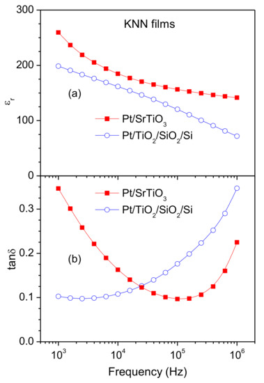
Figure 1.
Frequency dependence of the relative dielectric permittivity εr (a) and dissipation factor tan δ (b) of K0.5Na0.5NbO3 (KNN) films on Pt/TiO2/SiO2/Si (open circles) and Pt/SrTiO3 substrates (solid squares) at room temperature.
Values of tan δ, revealing v-like variation with frequency for both kinds of substrates, are equal to 0.097 at the minima, although the minimum frequency is 2.5 kHz for Pt/TiO2/SiO2/Si, and 100 kHz for Pt/SrTiO3. However, for frequency that is usually measured by orders of magnitude and, therefore, presented in log scale, it is quite a moderate difference. At 25 kHz (the middle of our frequency window in log scale), the films deposited on Pt/TiO2/SiO2/Si reveal a tan δ of 0.126, while those deposited on Pt/SrTiO3 present a tan δ of 0.123, as shown in Table 1. εr of KNN films is higher in the whole frequency range for those deposited on Pt/SrTiO3, revealing, at 25 kHz, a value of 170 in comparison to εr of 146 for KNN films on Pt/TiO2/SiO2/Si, as summarized in Table 1, as well.

Table 1.
Room-temperature electrical characteristics of KNN films deposited on platinized Si and SrTiO3 substrates, including the dissipation factor (tan δ), the relative dielectric permittivity (εr) at 25 kHz, the remanent polarization (Pr) and the coercive field (Ec) at applied electric field of ~70 kV/cm, as well as presence of out-of-plane piezoelectric force microscopy (PFM) response.
Due to the relatively high losses and, therefore, some leakage contribution the polarization-electric field (P-E) dependences, measured at frequency of 50 Hz, reveal no saturation (see Figure S1, Supplementary Materials). Moreover, the loops grow with the increase of maximum electric field that is also typical for KNN films [15,19]. Despite that, Table 1 presents, as well, that under a field of ~70 kV/cm (the highest field at which the P-E loops could be measured), KNN thin films on Pt/TiO2/SiO2/Si show values of Pr and Ec of 2.65 μC/cm2 and 43.6 kV/cm, respectively, while the ferroelectric properties of the films identically deposited on Pt/SrTiO3 reach an almost doubled Pr of 4.56 μC/cm2, and a rather close Ec of 39.9 kV/cm.
Moreover, we could also observe a local piezoresponse for KNN films on Pt/SrTiO3 by PFM (see Figure S2, Supplementary Materials), although we were not able to get it for KNN films on Pt/TiO2/SiO2/Si substrates. Topological and out-of-plane PFM signal images shown in Figure S2a,b, respectively, demonstrate that KNN films on Pt/SrTiO3 substrates can be effectively poled, revealing a clear contrast in PFM amplitude independent on the topological variations, as presented also by profiles in Figure S2c. Furthermore, piezoelectric loops obtained for KNN films on Pt/SrTiO3 by PFM, and shown in Figure S2d, support the presence of out-of-plane polarization in these films, in contrast to KNN films on Pt/TiO2/SiO2/Si, as marked in Table 1 as well. Despite these loops are rather qualitative, and PFM is a microscopic technique, whereas the Pr values are obtained macroscopically, they confirm that an increase in Pr observed for KNN films on Pt/SrTiO3, in comparison to Pt/TiO2/SiO2/Si substrates, is, in fact, due to a stronger out-of-plane ferroelectric behavior, rather than to the higher losses at low frequencies.
To clarify the different dielectric and ferroelectric responses of KNN thin films identically deposited on Pt/TiO2/SiO2/Si and Pt/SrTiO3 substrates, structural and microstructural analysis of these films was performed. From the PFM topological images, shown in Figure 2a,b, the root mean square (RMS) roughness of both kinds of films is estimated to be about 11 nm, as shown in Table 2. SEM cross-section and top-view micrographs of the produced KNN films are presented in Figure 3. From the top-view images, both kinds of films reveal a dense and crack-free microstructure with a smooth surface and ~100 nm grain size, as shown in Table 2 as well. From the cross-section micrographs, the thickness of the KNN films is ~335 nm, both for Pt/TiO2/SiO2/Si and Pt/SrTiO3 substrates, as also listed in Table 2. Thus, both kinds of films are rather identical, as in the roughness and thickness, as in the grain size and microstructure. Moreover, EDS analysis, presented in Figure 3c, indicates that potassium and sodium concentrations of both kinds of the prepared films are very close, revealing values within error bars. Estimated Nb content is close to the sum of the Na and K ones, thus, indicating the proximity of the film composition to the stoichiometric one.
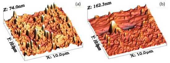
Figure 2.
Topography of KNN thin films deposited on Pt/SiO2/TiO2/Si (a) and Pt/SrTiO3 (b) substrates.
Table 2.
Film root mean square (RMS) roughness, average thickness, grain size, Lotgering factor, residual stress, and theoretical thermal stress for KNN films deposited on platinized Si and SrTiO3 substrates.
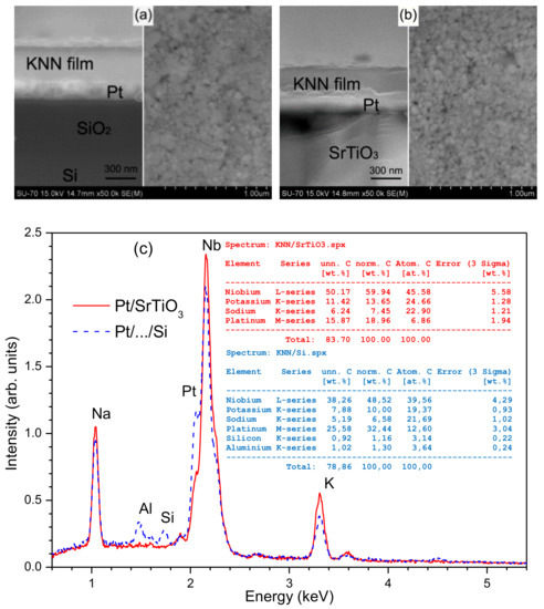
Figure 3.
Cross-section (left) and top-view (right) SEM micrographs of KNN films on Pt/TiO2/SiO2/Si (a) and Pt/SrTiO3 (b) substrates, as well as their energy-dispersive spectra with quantifications (c).
For the phase formation and assemblage analysis of KNN thin films, XRD measurements were performed as illustrated in Figure 4a. According to the diffraction peaks of the standard Na0.5K0.5NbO3 powder samples (JCPDS #01-079-7690), all the films have a well-crystallized perovskite phase. No other phases were detected besides some substrate reflections, although reflections at 2θ = 27.4° can also be related to a small amount of alkali-deficient K4Nb6O17 phase [12]. In general, KNN films have a tendency for preferential growth in (100) pseudo-cubic crystallographic direction [13,16,21]. XRD patterns can be used to quantify the film crystallographic texture, calculating the Lotgering factor (f)
where and with and being the intensities of (hkl) peaks for the textured and randomly oriented KNN thin films, respectively. As Table 2 also displays, the f(100) is 15.03% for KNN thin films deposited on Pt/SrTiO3 and, in the case of KNN films deposited on Pt/TiO2/SiO2/Si, it is 15.85%. These results are, again, very close, and confirm a rather random orientation of both KNN thin films, being in agreement with the moderate intensity of the (200) peaks.
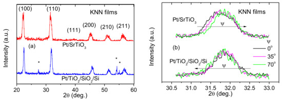
Figure 4.
XRD profiles in 20°–60° 2θ range (a), and around (110) peak of KNN at different tilt angles ѱ used for stress calculations (b) of KNN films on Pt/SrTiO3 and Pt/TiO2/SiO2/Si substrates at room temperature. Diffraction peaks of KNN phase are marked by corresponding indexes, while those from substrate are marked as * in (a).
Strain measurements were conducted by the XRD sin2 ѱ method, using a (110) diffraction peak of KNN, as shown in Figure 4b. In this method, the lattice spacings d of a specific (hkl) plane are determined at different tilt angles ѱ (inclined exposure), resulting in dѱ values normalized to the spacing at zero angle d0. Since the peak position moves in different directions with increasing ѱ, as presented in Figure 4b, the corresponding strains induced in the KNN films, by the Pt/TiO2/SiO2/Si and Pt/SrTiO3 substrates, are also different (see Figure S3, Supplementary Materials). KNN films deposited on Pt/SrTiO3 have a compressive strain, while the strain of KNN films deposited on Pt/TiO2/SiO2/Si is tensile. Using the normalized values of the obtained strain, the in-plane stress values can be calculated as
where Y and ѵ corresponds to the Young’s modulus and Poisson’s ratio of the film, respectively, and m is the gradient of the (dψ − d0)/d0 vs. sin2 ψ dependence. The values of KNN Young’s modulus of 104 GPa and Poisson’s ratio of 0.27 were used [24,25], resulting in a positive stress value of 234 MPa for KNN films deposited on Pt/TiO2/SiO2/Si, and a negative one of −450 MPa for the films on Pt/SrTiO3, as summarized in Table 2.
Thermal stress that originates between the film and substrate during cooling from the annealing to RT, due to the differences in their CTE, have been shown theoretically [26] and experimentally [22] to be the main component of the residual stress in non-epitaxial films deposited on metalized substrates. It can be calculated as
where αf(T) and αsub(T) are the temperature dependence of the CTE of KNN films and corresponding substrate [22]. According to the supplier information, CTE of Pt/TiO2/SiO2/Si substrates is 2.3 × 10⁻⁶ K−1, while that of SrTiO3 is 9 × 10⁻⁶ K−1. Comparing with the average CTE of 4.72 × 10⁻⁶ K−1 reported for KNN [27], a tensile thermal stress of 252 MPa is expected to occur at RT in KNN films deposited on Si substrates at 750 °C, while a compressive thermal stress of −445 MPa should be induced on SrTiO3 substrates. These values are also shown in Table 2, revealing a complete agreement with the measured residual stress values. Thus, thermal stress is, indeed, the main component of the residual stress for KNN films obtained in this work.
Then, for KNN films on Pt/TiO2/SiO2/Si, the film lattice is under tensile stress/strain induced on cooling from the annealing temperature due to the thermal expansion mismatch (αSi < αKNN), thus favoring the in-plane Nb ionic displacements responsible for ferroelectric properties [28], and lowering the out-of-plane polarization, similarly to SrTiO3 films on Al2O3 substrates [22], as well as Pb(Zr,Ti)O3 (PZT) thick and thin films of Si substrates [29,30]. For KNN films on Pt/SrTiO3, the film lattice is compressed in plane (αSrTiO₃ > αKNN). Therefore, a lattice distortion allowing the Nb ionic displacements dominantly out-of-plane is induced. As a result, the ferroelectric properties of these films are enhanced in the parallel-plate-capacitor configuration, yielding the superior polarization, similarly to SrTiO3 films on MgO substrates [22], PZT thick films on Al2O3 substrates [29] and PZT thin films of SrTiO3 substrates [30].
Concerning the dielectric permittivity, it should decrease with enhanced polarization, suggesting increased transition temperature (at which the permittivity exhibits the maximum and polarization is zero) and larger difference between that and the measurement temperature. Such variation was observed in epitaxial PZT films on SrTiO3 in comparison to Si substrates [30]. However, in polycrystalline films, simultaneous increase in the polarization and permittivity was reported for PZT thick films on Al2O3 in comparison to Si substrates [29], and for SrTiO3 thin films on MgO in comparison to Al2O3 substrates [22], similarly to the observations in this work. The reasons behind that can be slightly enlarged grain size in the in-plane compressed films, or some grain boundary-related mechanism yet to be investigated. Thus, in this work, we have demonstrated that, besides the alkali excess amount and annealing conditions, the coefficient of thermal expansion of the substrate can also contribute to the final electrical properties of polycrystalline KNN thin films.
In conclusion, the influence of stress/strain built during KNN films’ processing on their electrical properties, is studied in this work. For this purpose, identical polycrystalline crack-free ~335 nm-thick KNN films were produced from 0.2 M precursor solutions with 5% of potassium excess by RTA at 750 °C on platinized Si and SrTiO3 substrates. Using XRD analysis, KNN thin films were found to have a perovskite structure without clear preferential orientation. Moreover, KNN thin films deposited on Pt/TiO2/SiO2/Si substrates are found to be under a tensile in-plane stress, while KNN films deposited on Pt/SrTiO3 substrates are under compressive stress, with values correlating very well with the stress calculated to appear in KNN thin films on cooling from the annealing temperature, due to the thermal expansion mismatch. As a result of the corresponding lattice distortions, determining displacement of Nb5+ ions, the room-temperature ferroelectric measurements in the parallel-plate-capacitor geometry indicated an increase in the Pr value for KNN films under compressive strain deposited on Pt/SrTiO3 substrates, compared to the films under tensile strain deposited on Pt/TiO2/SiO2/Si, while impedance spectroscopy measurements revealed enhanced εr. Thus, it is shown that variation of εr and Pr of KNN-based sol–gel thin films can be achieved by controlling the strain/stress level on the films via the choice of the substrate.
Supplementary Materials
The following are available online at http://www.mdpi.com/2079-6412/8/12/449/s1, Figure S1: polarization (P)-electric field (E) loops of KNN films deposited on Pt/SrTiO3 (solid line) and Pt/TiO2/SiO2/Si substrates (dash line) measured at room temperature and 50 Hz under electric field up to 45 (a), 60 (b) and 75 kV/cm (c), Figure S2: topography (a), out-of-plane PFM signal (b), cross-section profile of topography and PFM amplitude (c) and local piezoelectric hysteresis loops (d) of KNN thin films deposited on Pt/SrTiO3 substrates. No out-of-plane piezoresponse could be obtained for KNN films on Pt/TiO2/SiO2/Si substrates, Figure S3: strain (dψ − d0)/d0 of KNN films on Pt/TiO2/SiO2/Si (open circles) and Pt/SrTiO3 substrates (solid squares) as a function of sin2 ψ together with linear fits used for stress calculations at room temperature.
Author Contributions
Conceptualization, P.M.V. and M.E.C.; Methodology, S.Z, R.S. and O.O.; Software, R.S.; Validation, O.O. and S.Z.; Formal Analysis, A.S., I.B. and A.T.; Investigation, A.S and I.B.; Resources, A.T, P.M.V, O.O., M.E.V.; Data Curation, A.T. and A.S.; Writing—Original Draft Preparation, A.S and A.T.; Writing—Review and Editing, A.T., P.M.V. and M.E.C.; Visualization, A.T. and A.S.; Supervision, A.T.; Funding Acquisition, A.T. and I.B.
Funding
This work was funded by FEDER funds via Programa Operacional Factores de Competitividade—COMPETE and National funds via FCT (Fundação para a Ciência e a Tecnologia) within the Project CICECO-FCOMP-01-0124-FEDER-037271 (FCT PEst-C/CTM/LA0011/2013) as well as within FCT independent researcher grants (IF/00602/2013 and IF/00582/2015).
Acknowledgments
M.R. Soares and M. Ferro are acknowledged for XRD strain measurements and EDS analysis, respectively.
Conflicts of Interest
The authors declare no conflict of interest.
References
- Li, J.F.; Wang, K.; Zhu, F.Y.; Cheng, L.Q.; Yao, F.Z. (K,Na)NbO3-based lead-free piezoceramics: Fundamental aspects, processing technologies, and remaining challenges. J. Am. Ceram. Soc. 2013, 96, 3677–3696. [Google Scholar] [CrossRef]
- Saito, Y.; Takao, H.; Tani, T.; Nonoyama, T.; Takatori, K.; Homma, T.; Nagaya, T.; Nakamura, M. Lead-free piezoceramics. Nature 2004, 432, 84–87. [Google Scholar] [CrossRef] [PubMed]
- Rafiq, M.A.; Costa, M.E.; Tkach, A.; Vilarinho, P.M. Impedance analysis and conduction mechanisms of lead free potassium sodium niobate (KNN) single crystals and polycrystals: A comparison study. Cryst. Growth Des. 2015, 15, 1289–1294. [Google Scholar] [CrossRef]
- Rafiq, M.A.; Tkach, A.; Costa, M.E.; Vilarinho, P.M. Defects and charge transport in Mn-doped K0.5Na0.5NbO3 ceramics. Phys. Chem. Chem. Phys. 2015, 17, 24403–24411. [Google Scholar] [CrossRef] [PubMed]
- Rodel, J.; Webber, K.G.; Dittmer, R.; Jo, W.; Kimura, M.; Damjanovic, D. Transferring lead-free piezoelectric ceramics into application. J. Eur. Ceram. Soc. 2015, 35, 1659–1681. [Google Scholar] [CrossRef]
- Blomqvist, M.; Koh, J.-H.; Khartsev, S.; Grishin, A.; Andreasson, J. High-performance epitaxial Na0.5K0.5NbO3 thin films by magnetron sputtering. Appl. Phys. Lett. 2002, 81, 337–339. [Google Scholar] [CrossRef]
- Kim, J.S.; Lee, H.J.; Lee, S.Y.; Kim, I.W.; Lee, S.D. Frequency and temperature dependence of dielectric and electrical properties of radio-frequency sputtered lead-free K0.48Na0.52NbO3 thin films. Thin Solid Films 2010, 518, 6390–6393. [Google Scholar] [CrossRef]
- Li, T.; Wang, G.; Li, K.; Du, G.; Chen, Y.; Zhou, Z.; Remiens, D.; Dong, X. Electrical properties of lead-free KNN films on SRO/STO by RF magnetron sputtering. Ceram. Int. 2014, 40, 1195–1198. [Google Scholar] [CrossRef]
- Suenaga, K.; Shibata, K.; Watanabe, K.; Nomoto, A.; Horikiri, F.; Mishima, T. Effect of lattice strain and improvement of the piezoelectric properties of (K,Na)NbO3 lead-free film. Jpn. J. Appl. Phys. 2010, 49, 09MA05. [Google Scholar] [CrossRef]
- Khartsev, S.; Grishin, A.; Andreasson, J.; Koh, J.H.; Song, J.-S. Comparative characteristics of Na0.5K0.5NbO3 films on Pt by pulsed laser deposition and magnetron sputtering. Integr. Ferroelectr. 2003, 55, 769–779. [Google Scholar] [CrossRef]
- Abazari, M.; Akdogan, E.K.; Safari, A. Dielectric and ferroelectric properties of strain-relieved epitaxial lead-free KNN-LT-LS ferroelectric thin films on SrTiO3 substrates. J. Appl. Phys. 2008, 103, 104106. [Google Scholar] [CrossRef]
- Tanaka, K.; Hayashi, H.; Kakimoto, K.I.; Ohsato, H.; Iijima, T. Effect of (Na,K)—Excess precursor solutions on alkoxy-derived (Na,K)NbO3 powders and thin films. Jpn. J. Appl. Phys. 2007, 46, 6964–6970. [Google Scholar] [CrossRef]
- Ahn, C.W.; Lee, S.Y.; Lee, H.J.; Ullah, A.; Bae, J.S.; Jeong, E.D.; Choi, J.S.; Park, P.H.; Kim, I.W. The effect of K and Na excess on the ferroelectric and piezoelectric properties of K0.5Na0.5NbO3 thin film. J. Phys. D Appl. Phys. 2009, 42, 215304. [Google Scholar] [CrossRef]
- Yan, X.; Ren, W.; Wu, X.; Shi, P.; Yao, X. Lead-free (K,Na)NbO3 ferroelectric thin films: Preparation, structure and electrical properties. J. Alloy. Compd. 2010, 508, 129–132. [Google Scholar] [CrossRef]
- Kang, C.; Park, J.H.; Shen, D.; Ahn, H.; Park, M.; Kim, D.-J. Growth and characterization of (K0.5Na0.5)NbO3 thin films by a sol–gel method. J. Sol–Gel Sci. Technol. 2010, 58, 85–90. [Google Scholar] [CrossRef]
- Kupec, A.; Malic, B.; Tellier, J.; Tchernychova, E.; Glinsek, S.; Kosec, M. Lead-free ferroelectric potassium sodium niobate thin films from solution: Composition and structure. J. Am. Ceram. Soc. 2012, 95, 515–523. [Google Scholar] [CrossRef]
- Yu, Q.; Li, J.-F.; Sun, W.; Zhou, Z.; Xu, Y.; Xie, Z.-K.; Lai, F.-P.; Wang, Q.-M. Electrical properties of K0.5Na0.5NbO3 thin films grown on Nb:SrTiO3 single-crystalline substrates with different crystallographic orientations. J. Appl. Phys. 2013, 113, 024101. [Google Scholar] [CrossRef]
- Vendrell, X.; Raymond, O.; Ochoa, D.A.; Garcia, J.E.; Mestres, L. Growth and physical properties of highly oriented La-doped (K,Na)NbO3 ferroelectric thin films. Thin Solid Films 2015, 577, 35–41. [Google Scholar] [CrossRef]
- Deng, Q.; Zhang, J.; Huang, T.; Xu, L.; Jiang, K.; Li, Y.; Hu, Z.; Chu, J. Optoelectronic properties and polar nano-domain behavior of sol–gel derived K0.5Na0.5Nb1−xMnxO3−δ nanocrystalline films with enhanced ferroelectricity. J. Mater. Chem. C 2015, 3, 8225–8234. [Google Scholar] [CrossRef]
- Won, S.S.; Lee, J.; Venugopal, V.; Kim, D.-J.; Lee, J.; Kim, I.W.; Kingon, A.I.; Kim, S.-H. Lead-free Mn-doped (K0.5,Na0.5)NbO3 piezoelectric thin films for MEMS-based vibrational energy harvester applications. Appl. Phys. Lett. 2016, 108, 232908. [Google Scholar] [CrossRef]
- Weng, C.M.; Tsai, C.C.; Hong, C.S.; Lin, C.C.; Chen, C.C.; Chu, S.Y.; Sheen, J.; Chen, Z.Y.; Su, H.H. Effects of non-stoichiometry on the microstructure, oxygen vacancies, and electrical properties of KNN-based thin films. ECS J. Solid State Sci. Technol. 2016, 5, N49–N56. [Google Scholar] [CrossRef]
- Tkach, A.; Okhay, O.; Reaney, I.M.; Vilarinho, P.M. Mechanical strain engineering of dielectric tunability in polycrystalline SrTiO3 thin films. J. Mater. Chem. C 2018, 6, 2467–2475. [Google Scholar] [CrossRef]
- Okhay, O.; Tkach, A.; Nuzhnyy, D.; Petzelt, J.; Vilarinho, P.M. Polar phonons in polycrystalline SrTiO3 thin films: The role of the substrate. Ferroelectrics 2018, in press. [Google Scholar]
- Jeager, R.E.; Egerton, L. Hot pressing of potassium sodium niobates. J. Am. Ceram. Soc. 1962, 45, 209–213. [Google Scholar] [CrossRef]
- Egerton, L.; Dillon, D.M. Piezoelectric and dielectric properties of ceramics in the system potassium sodium niobate. J. Am. Ceram. Soc. 1959, 42, 438–442. [Google Scholar] [CrossRef]
- Zhang, J.; Weiss, C.V.; Alpay, S.P. Effect of thermal stresses on the dielectric properties of strontium titanate thin films. Appl. Phys. Lett. 2011, 99, 042902. [Google Scholar] [CrossRef]
- Malic, B.; Razpotnik, H.; Koruza, J.; Kokalj, S.; Cilensek, J.; Kosec, M. Linear thermal expansion of lead-free piezoelectric K0.5Na0.5NbO3 ceramics in a wide temperature range. J. Am. Ceram. Soc. 2011, 94, 2273–2275. [Google Scholar] [CrossRef]
- Levin, I.; Krayzman, V.; Cibin, G.; Tucker, M.G.; Eremenko, M.; Chapman, K.; Paul, R.L. Coupling of emergent octahedral rotations to polarization in (K,Na)NbO3 ferroelectrics. Sci. Rep. 2017, 7, 15620. [Google Scholar] [CrossRef]
- Han, G.; Ryu, J.; Yoon, W.-H.; Choi, J.-J.; Hahn, B.-D.; Kim, J.-W.; Park, D.-S.; Ahn, C.-W.; Priya, S.; Jeong, D.-Y. Stress-controlled Pb(Zr0.52Ti0.48)O3 thick films by thermal expansion mismatch between substrate and Pb(Zr0.52Ti0.48)O3 film. J. Appl. Phys. 2011, 110, 124101. [Google Scholar] [CrossRef]
- Moalla, R.; Vilquin, B.; Saint-Girons, G.; Sebald, G.; Baboux, N.; Bachelet, R. Dramatic effect of thermal expansion mismatch on the structural, dielectric, ferroelectric and pyroelectric properties of low-cost epitaxial PZT films on SrTiO3 and Si. CrystEngComm 2016, 18, 1887–1891. [Google Scholar] [CrossRef]


© 2018 by the authors. Licensee MDPI, Basel, Switzerland. This article is an open access article distributed under the terms and conditions of the Creative Commons Attribution (CC BY) license (http://creativecommons.org/licenses/by/4.0/).