Abstract
A solvent-free, solid-state mechanochemical method was developed to synthesize the chalcohalide compound SbSI at room temperature. Dry high-energy planetary ball milling of elemental antimony, sulfur, and iodine produced a pure, stoichiometric polycrystalline SbSI powder with an orthorhombic structure. This powder was then sintered under mild thermal conditions to create dense targets. Amorphous SbSI thin films were subsequently deposited from these targets at room temperature using Pulsed Electron Deposition. The films maintained the correct stoichiometry and exhibited an optical bandgap of 1.89 eV. Post-deposition annealing at 90 °C in air successfully induced crystallization, demonstrating a viable, low-temperature, and eco-friendly route to produce polycrystalline SbSI thin films. This scalable approach has promising potential for optoelectronic and energy-harvesting applications.
1. Introduction
Technological innovation for green energy and optoelectronics industrial solutions is needed to bypass the state of the art in methodologies and performances, demanding an extra effort from researchers in material science for the synthesis, characterization and prototyping of more efficient materials and device solutions.
In this framework, the ternary pnictogen chalcohalides, commonly denoted as MChX (where M = Bi, Sb, As; Ch = S, Se, Te; X = I, Br, Cl, F), have gained significant attention thanks to their unique properties which make them suitable for a wide variety of applications. Examples include ionizing radiation detectors based on BiSI, BiOI sonocatalyst and BiOCl catalysts, laser technologies for civil applications based on Sn7Br10S2, BiSCl, BiSBr, BiSI, BiSeI, BiSeBr and BiSeCl-based microwave oscillators [1,2,3,4,5].
Among them, antimony sulphoiodide (SbSI) still stands as one of the most-known representatives of these compounds. SbSI exhibits a highly anisotropic crystal structure, defined by double chains [(SbSI)∞]2 composed of two chains connected through a twofold screw axis and linked via short and strong Sb–S bonds. These double chains are held together by weak van der Waals interactions, giving SbSI crystals low mechanical strength and a tendency to form needle-like shapes [6].
SbSI exhibits significant structural polymorphism induced by displacive transformations of its orthorhombic symmetry which are very close in free energy and determine the formation of ferroelectric phase Pna21 below TC1 = 298 K (experimental Curie Temperature), an antiferroelectric phase P212121 in the temperature range from 298 K to TC2 = 410 K, and a paraelectric phase Pnam above 410 K [7].
This structural peculiarity endows SbSI with a remarkable set of properties, including the phenomenon of pyroelectricity, which arises from its temperature-dependent ferroelectric polarization. Furthermore, the transition of dipoles into ferroelectric materials induces a field-dependent volume change, thereby rendering SbSI piezoelectric. Consequently, SbSI manifests a plethora of intriguing properties, including electromechanical, electrocaloric, and non-linear optical characteristics. These properties depend on the applied electric field, temperature, or strain. It is evident that these features confer upon SbSI considerable application potential in a multitude of devices, including piezoelectric nanogenerators, photonic crystals, photodetectors and ferroelectric random-access memories (FERAM) [8,9,10,11].
Nevertheless, one of the most notable properties of SbSI is its photovoltaic response, arising from an indirect optical bandgap of 1.86 eV [12]. This feature allows efficient sunlight absorption along with mild electrical conductivity, making SbSI a promising candidate for next-generation energy applications [13]. The combination of ferroelectric and photovoltaic behavior renders SbSI a so-called ferro-photovoltaic (FE-PV) material. The FE-PV effect is responsible for the generation of a steady PV response (photocurrent or photovoltage) along the polarization direction in ferroelectric materials, obviating the necessity for a p-n junction. In recent years, interest in materials exhibiting this effect has grown substantially, with numerous studies reporting efforts to design FE-PV devices based on compounds such as BiFeO3, BaTiO3, and Pb(Zr,Ti)O3 [14,15,16,17]. In this specific case, the ferroelectric state of SbSI is characterized by a low coercive field (EC = 100 V/cm at 0 °C) and a high saturation polarization (Ps = 25 μC/cm2), while its transport properties exhibit relatively high charge mobility [18,19].
Different approaches for the synthesis of SbSI crystals have been reported in the literature so far, including vertical Bridgman technique [20], sintering of antimony trisulfide (Sb2S3) and antimony triiodide (SbI3) [21], hydrothermal processes [22], chemical vapor deposition [23] and sonochemical [24] synthesis routes. However, most of the current synthesis methods require elevated temperatures and pressures during the process. In addition, the utilization of toxic solvents or gases is a common practice in many of the aforementioned methods, which invariably lead to the production of hazardous by-products.
In this paper, we present a detailed synthesis route for the large-scale and cost-effective production of SbSI powders via mechanochemical (MC) reactions, showing a novel approach for developing functional SbSI FE-PV devices. According to the literature, MC synthesis through high energy ball milling process has been found to be an effective method for the synthesis of other semiconductors, such as chalcogenides for PV applications. In our case, similarly to what was observed for CuInS2 (CIS) [25], we provide further evidence that a straightforward two-step sintering process can be applied to densify the MC powders, to obtain a target suitable for SbSI thin-film deposition by Pulsed Electron Deposition (PED): this latter method has already well demonstrated the ability to stoichiometrically transfer even complex-phase materials in a high-quality thin film form, such as multiferroic oxides, multinary chalcogenides and ultra-wide bandgap semiconductors [26,27,28]. The successful synthesis of SbSI crystals by MC, as well as the use of the PED technique for the deposition of SbSI thin films, are the most innovative results of the present report. Our findings are supported by a comprehensive characterization of the morphological, compositional, and optical properties of this material, accompanied by the formulation of a methodology for the synthesis of crystalline SbSI from amorphous films deposited by PED. This research may lead to a substantial advancement in the development of functional SbSI FE-PV devices realized respecting the criteria of sustainability, i.e., by using a low-energy consuming and eco-friendly synthesis route.
2. Materials and Methods
Mechanochemical solid state reactions were performed in air atmosphere and without the addition of any liquid solvents, using a Pulverisette 7 Classic Line planetary ball mill (Fristch GmbH, Idar-Oberstein, Germany), with agate or yttrium-stabilized zirconia mill pots (volume: 45 mL) and spheres of the corresponding material (diameter: 10 mm). A stoichiometric ratio of elementary Antimony (Alfa Aesar, Ward Hill, MA, USA, 99.99% purity), Sulfur (ThermoFisher, Waltham, MA, USA, >99.5% purity) and Iodine (ChemPur, Karlsruhe, Germany, 99.99% purity) was used to prepare the precursors by manually grinding the powdered reactants with an agate mortar, until color homogeneity of the mixture is reached. The MC reactions were studied by varying the combination of the main parameters: (i) rotational speed (RPM), (ii) ball-to-powder mass ratio (BPR), (iii) reaction time (TIME) and (iv) the hardness of mechanical media.
SbSI films have been deposited using a high-vacuum chamber equipped with a Pulsed Electron Deposition commercial source (PEBS-20, Neocera Inc., Beltsville, MD, USA), pumped down to a base pressure of ~2.0 × 10⁻⁴ Pa. The pulsed e-beam was ignited at a discharge voltage of 16 kV. Pulse repetition rate was fixed at 10 Hz. During the deposition process, Ar gas (5 N purity) was introduced at a pressure of about 3.0 × 10⁻¹ Pa for igniting the electron beam and stabilizing the beam propagation towards the target. As target material, we utilized the pellet produced from MC powders, as described in detail later in the results section. The films were deposited onto 2.5 × 2.5 cm2-wide bare soda–lime glass substrates, coated with fluorine-doped tin oxide (FTO). The commercial conductive substrates were cleaned in an ultrasonic bath of acetone, ethanol and isopropanol, with a duration of three minutes for each treatment. They were dried using 5 N Ar flow, then placed on a hot plate set at 200 °C for 5 min and finally mounted on the holder. Target-substrate distance was fixed at 8 cm. Substrates were first mounted in a load-lock chamber, then transferred inside the main chamber and left over a graphite susceptor heated by halogen lamps. Substrate temperature varied from room temperature (RT) to 300 °C, monitored by a type-K thermocouple.
The structural analysis was performed by Powder X-Ray Diffraction (PXRD); the phase identification was carried out on data measured using a Rigaku Smartlab XE diffractometer (Rigaku Corporation, Tokyo, Japan) in Bragg–Brentano geometry with Cu Kα radiation (Kα1 = 1.54059 Å; Kα2 = 1.54441 Å; Kα2/Kα1 = 0.497). A Ni filter was used to suppress the Kβ contribution. 5.0° soller slits were both located on incident and diffracted beam; PXRD data were collected using a HyPix3000 detector (Rigaku Corporation, Tokyo, Japan) operating in 1D mode. In the case of the ab initio structure determination process, PXRD data were measured by a Rigaku RINT2500 rotating anode diffractometer (Rigaku Corporation, Tokyo, Japan; 50 kV, 200 mA) equipped with a silicon strip Rigaku D/teX Ultra detector (Rigaku Corporation, Tokyo, Japan). An asymmetric Johansson Ge(111) crystal was used to select the monochromatic Cu Kα1 radiation (λ = 1.54056 Å). Measurements were executed in transmission mode by introducing the sample powder in a Lindemann glass capillary tube with a diameter of 0.5 mm. The XRPD patterns were recorded in the 2θ range 10.0–120.0° by step scanning, with 2θ increments of 0.02° and a fixed counting time of 2 s/step.
The morphology and composition of the samples were investigated with a field-emission Scanning Electron Microscope (SEM, Zeiss AURIGA Compact, Zeiss, Oberkochen, Germany), equipped with an Energy-Dispersive X-ray analysis (EDX, Xplore 30, Oxford Instruments, Abingdon, UK). SEM images were acquired with different acceleration voltages (5–10 kV) of the primary electron beam and collected with a standard Everhart-Thornley detector. EDX analyses were conducted by using a 20 kV accelerated primary electron beam. Thin-film cross-sections were analyzed through Focused Ion Beam technique (FIB, Zeiss AURIGA Compact, Zeiss, Oberkochen, Germany) using a Ga+ ion beam with an acceleration voltage of 30 kV and a current of 50 pA.
Confocal Raman measurements were obtained at 25 °C using a Horiba LabRAM HR Evolution confocal spectrometer (Horiba Ltd, Kyoto, Japan), using a configuration with a 600 lines/mm grating, a set of Bragg ultra-low frequency filters for the rejection of the Rayleigh scattering and a liquid nitrogen-cooled CCD detector. The 633-laser line was used for excitation. Following a thorough evaluation of the optimal conditions for safeguarding the samples from thermal degradation, the laser power was set <1 mW. An optical 100× objective was used to obtain a spatial resolution of about 1 μm, with 0.5 cm−1 resolution. Typical collection time for the confocal configuration was 15 s for each acquisition, with 4 repetitions.
X-ray photoelectron spectroscopy (XPS) was performed using a Thermo Scientific ESCALAB QXi spectrometer (Thermo Fischer Scientific Inc., Waltham, MA, USA), equipped with both non-monochromatic twin anode (Al/Mg) and monochromatic Al Kα radiation sources (1486.6 eV). During the analysis, the temperature of room was 300 (±1) K. The analysis of the SbSI target sample with the Al monochromatic source was hindered by differential surface charging strongly affecting spectra reproducibility. Several attempts were made to identify the optimal conditions to minimize this effect. Differential charging was successfully eliminated by mounting a few milligrams of SbSI target powder using double-sided adhesive carbon tape onto a sample holder grounded to the instrument, while applying charge compensation and employing the non-monochromatic Al X-ray source. Charge compensation was applied by beams of combined low energy ion (Ar+) and electron beams. The SbSI thin film deposited on a FTO substrate was analyzed using the monochromatic Al Kα X-ray source in the absence of charge compensation. High resolution spectra were recorded using a constant pass energy (20 eV), at 0.1 eV/step, with a dwell time of 50 ms. Depth profiling was performed by means of monoatomic ion (Ar+) beam at 2000 eV and a raster size of 3.25 × 3.25 mm2. XPS peak fittings were performed in the framework of the Avantage software (Avantage 6.10.0.59) after background correction with the smart-background function implemented in the same software using pseudo-Voigt functions for the synthetic peaks.
Atomic force microscopy (AFM) measurements were carried out using a Park Scientific XE-100 system (Park Systems Corp., Suwon-si, Gyeonggi-do, South Korea) operating in non-contact mode. For morphological characterization, scans were performed over a 20 × 20 µm2 area at a scan frequency of 0.3 Hz.
3. Results
3.1. Mechanosyntesis of SbSI Powders
The exploited solid-state MC reaction among the SbSI elemental precursors is the following:
2Sb + 2S + I2 → 2SbSI
High-energy ball milling parameters (BPR, RPM, TIME and hardness/density of the mechanical media) were varied to maximize the purity and the mass amount of final product while ensuring the correct stoichiometry of the material. A set of five distinct powder samples (named A–E) was obtained through the variation in the parameters, as listed in Table 1, and phase identification was performed by collecting their X-ray powder diffraction patterns. It is found that the process can be carried out in air under ambient pressure, as the presence of oxygen does not lead to the formation of spurious oxides or undesired oxidation processes. The mechanical activation barrier for this reaction is determined to be significantly high, as the onset of the reaction requires a combination of high rotational energies (≥600 RPM) and extended milling times (≥12 h) to activate the less reactive precursor (Sb).

Table 1.
List of powder samples produced by varying the parameters of MC synthesis.
A solution to fully overcome the activation barrier is to enhance the hardness of the jar and sphere materials. In fact, when agate (SiO2, Mohs hardness = 6.5–7) is used, the SbSI phase fails to form, regardless of RPM and milling time. XRD patterns displayed in Figure S1 report that in samples A and B, obtained using agate mechanical media, only unreacted Sb and SbI3 powders are produced. When a harder material such as Yttria-stabilized Zirconia (Y:ZrO2, Mohs hardness = 7.5) is used, SbSI phase begins to form at BPR = 14, RPM = 600, and prolonging milling times (samples C and D). The BPR value of 14 was then set as invariant because it was established sufficiently high to activate the reaction while it is small enough to minimize the impact statistics between balls. Under these conditions, the collision and sliding of the balls against the reactants ‘s powder distributed over the jar walls represent the predominant mechanical energy transfer mechanism. This choice also allowed the minimization of the erosion of the Y:ZrO2 spheres thus making the contamination of the final product negligible. Finally, complete formation without reagent residue is achieved by increasing the RPM value above 650 using Y:ZrO2 (sample E; Figure 1).
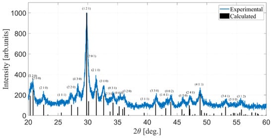
Figure 1.
XRD pattern of the optimized MC powders of SbSI (Sample E, blue curve) and the corresponding calculated diffraction peaks (black bars, ICSD ref. #30023).
The optimal configuration to selectively obtain a pure phase of SbSI was found to be 650 RPM, 14 BPR, and TIME = 20 h (divided into 5 cycles of 4 h each) using Y:ZrO2. Noteworthily, the process has been established fixing the initial mass of precursors between 4 and 5 g (equivalent to 2 and 2.5 g per jar). This choice is needed in order to obtain the amount of material necessary to produce a 1”-large target from a single MC synthesis.
After the MC reaction, the grayish precursors mixture is transformed into a red powder. PXRD analysis indicates that the sample is a single-phase polycrystalline product, with no detectable impurities within the technique’s detection limit. The material exhibits low crystallinity, consistent with the expected characteristics of the MC synthesis technique (Figure 1). This experimental pattern matches the reference pattern of SbSI, both considering the paraelectric space group Pnam and the ferroelectric Pna21.
Unlike the findings reported by Kikuchi et al., based on single-crystal diffraction data [29], the analysis of powder diffraction data is unable to differentiate between the two space groups of the paraelectric and ferroelectric phases, since it relies mainly on detecting systematic absences in the set of integrated peak intensities. Both Pnam and Pna21 are characterized by the same systematic extinctions as they belong to the same extinction group Pna- and their lattice parameters and atomic positions are similar [29].
Consequently, the unambiguous assignment of the space group from powder diffraction data is impossible. This is confirmed by solving the crystal structure ab initio in both space groups, followed by the Rietveld refinement of the corresponding structure models over the 2θ range of 17–120°, using the software EXPO (EXPO Version 2.3.9) (see also Tables S1 and S2) [30]. The results at the end of the Rietveld refinement process are shown in Figure 2. The corresponding Rp and Rwp agreement factors are the following ones:
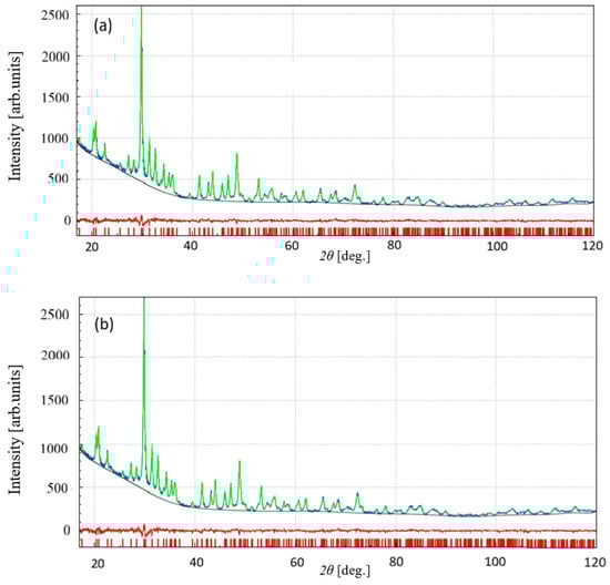
Figure 2.
Rietveld refinement results, obtained in (a) Pnam and (b) Pna21 using the EXPO package, showing the calculated (green), observed (blue), difference (red) pattern and the calculated 2θ-position of reflections (red vertical bars at the bottom).
The refined structure models in Pnam and Pna21 are strongly similar, characterized by a Root Mean Square Deviation (RMSD) value of 0.05 Å, where RMSD is defined as sqrt (∑idi2/Nau), i.e., the square root of the averaged squared distances between couples of corresponding atoms in the two compared models, with Nau the number of atoms in the asymmetric unit. In the case of Pnam, a further investigation carried out by the software FullProf (Version 5.20, December 2023) (see Figure S2) provides an estimate of the average size of crystallites (i.e., ~270 Å) [31]. Additional details on the ab initio structure determination process are described in the Supplementary Information.
Contrary to the PXRD technique, Raman spectroscopy can easily differentiate the two distinct phases of SbSI, showing well-distinguished vibrational modes corresponding to the ferroelectric and paraelectric/antiferroelectric phases. The primary differences between the spectra of the two structures are mainly observed in the low-frequency region (υ < 75 cm−1). For T < TC2, in the paraelectric phase, some of the lines are no longer Raman active and the low frequency region of the spectrum is considerably simplified if compared to the ferroelectric phase spectrum [32].
Figure 3 displays the Raman spectrum of optimized MC powders: the measured Raman peaks are found at 39 cm−1, 52 cm−1, 69 cm−1, 105 cm−1, 138 cm−1, 215 cm−1, and 319 cm−1. It is evident that these positions are consistent with those reported in the literature for the paraelectric phase, as illustrated in Table 2.
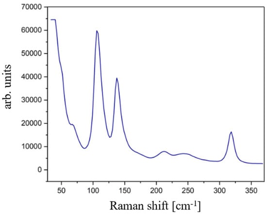
Figure 3.
Raman spectrum of the optimized MC powders.
Table 2.
Raman Active vibrational modes of SbSI in the paraelectric phase (at 25 °C) and in the ferroelectric phase (at −70 °C) corresponding, respectively, to the irreducible representation Γ1 + Γ7 and Γ1 + Γ2 [32].
In conclusion, it can be hypothesized that the specific MC synthesis route appears to meta-stabilize the paraelectric phase within the thermal range where antiferroelectric phase is expected to be observed.
The crystalline morphology and chemical composition of the SbSI powders were determined using SEM/EDX analysis, which revealed that the particles synthesized via MC were unevenly distributed in shape and size, with average sizes spanning from tens of nanometers to a few micrometers (Figure 4).
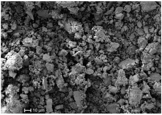
Figure 4.
SEM image of the mechanochemically synthesized SbSI powders.
The EDX analysis reported in Table 3 confirms, within the experimental uncertainty, that the elemental composition of the synthesized powders corresponds to the nominal stoichiometric ratio (within the instrument’s margin of error) for SbSI, exhibiting an approximated 1:1:1 ratio of Sb:S:I. No traces of Zr were revealed, suggesting that the erosion of pots and balls during the milling process was minimal.
Table 3.
Atomic content of SbSI powders, targets and films, measured by EDX and XPS techniques. The estimated relative error is approximately 5% for the EDX data and 1% for the XPS measurements.
3.2. Fabrication of SbSI Targets for Pulsed Electron Deposition
For the target preparation, 4–5 g of SbSI powders obtained by a single MC synthesis is sintered by cold pressing in a cylindrical pellet die mold at 200 bars for 1.5 h. The pressed powders are then annealed at different temperatures in a quartz tube under N2 inert atmosphere to achieve a degree of density in line with PED requirements.
The effects of varying annealing temperatures in quartz tubes on the production of high-degree crystallinity and adequate density in the target material have been investigated. From the XRD analysis, the crystallization process is activated at temperatures higher than 100 °C, as evidenced by the reduction in the FWHM of the peaks (Figure 5, pink curve), whereas lower temperatures do not result in a significant enhancement of crystallinity (yellow curve) compared to untreated SbSI powders. However, at temperatures exceeding 125 °C, the material begins to deteriorate, resulting in a partial sublimation of the more volatile elements, S and I, which, in turn, leads to a broadening of the XRD peaks and an increase in the noise levels detected during the measurement (green curve). This implies that the stability range of the MC SbSI is extremely narrow at ambient pressure. The maximum degree of crystallinity that can be achieved with this treatment is obtained at an annealing temperature of 125 °C for 16 h; after such time, no morphological improvement is detected.
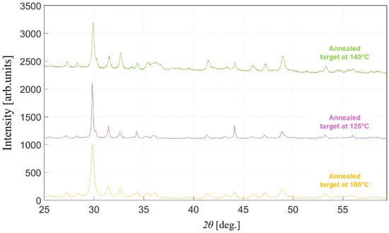
Figure 5.
XRD patterns of the MC SbSI target treated at different annealing temperatures for 16 h.
A direct comparison between the XRD pattern of the target (blue curve) and the as-obtained MC powders (red curve) is presented in Figure 6, clearly showing the formation of a more crystalline phase in the final target. Indeed, thanks to an increase in the signal-to-noise ratio and a decrease in the peak broadening, the less intense peaks in the doublets attributable to the pairs of reflections (120)/(200), (121)/(201), (040)/(320), and (002)/(150), hidden in the black curve, are well resolved in the pink curve.
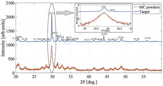
Figure 6.
XRD patterns of the mechanochemically synthesized SbSI powder (red curve) and of the sintered target treated at 125 °C for 16 h (blue curve). The inset highlights the width of the main (121) reflection peak.
The target density, calculated from the ratio between the final disk weight and its volume, is 3.7 g/cm3, which is approximately 21% lower than the nominal single-crystal density of SbSI (i.e., 4.65 g/cm3) [33]. This is a favorable outcome in view of its utilization for PED, since this technique requires not too high-density targets to optimize the material ablation and the film deposition [25].
The EDX compositional analysis shows that the stoichiometry of the target is retained after the annealing process (Table 3). SEM analysis points out that the surface is extremely regular, uniform and dense (Figure 7a), while the morphology of the material beneath the target surface is characterized by the presence of needle-shaped microstructures (Figure 7b).
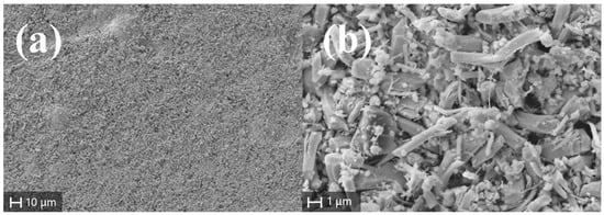
Figure 7.
SEM images of the annealed mechanochemically synthesized SbSI target: (a) planar view of the surface; (b) subsurface morphology.
The XPS analysis of the SbSI target was initially complicated by differential surface charging during photoelectron spectra acquisition. It should be emphasized that the XPS response of SbSI materials is intrinsically non-trivial. Grigas et al. reported splitting of core-level signals at the phase transition temperature (TC1) in SbSI single-crystal [34], with the effect intensifying with temperature and becoming particularly pronounced from 300 K. Even visible light irradiation significantly alters the core-level positions of SbSI single crystals in the ferroelectric phase [35]. In contrast, Ikemoto [36] observed no splitting in powder samples at RT (paraelectric phase), although charging-like phenomena with low reproducible spectra emerged upon cooling into the ferroelectric phase. When analyzing the SbSI target with a monochromatic X-ray source, charging-like effects were observed, leading to peak broadening and even splitting. These effects were spatially inhomogeneous and had low reproducibility along the target disk. Several approaches were tested to identify the most suitable measurement conditions for minimizing this behavior. Ultimately, differential charging was completely suppressed by using a non-monochromatic X-ray source in combination with charge compensation, as detailed in the Experimental Section. The high-resolution spectra for S 2p, Sb 3d and I 3d photoemission regions are reported in Figure 8. The binding energies (BE) of the S 2p3/2, Sb 3d5/2, and I 3d5/2 peaks were determined to be 161.8 eV, 530.1 eV, and 619.0 eV, respectively. These values are consistent with the sulfide and iodide environments expected for the SbSI matrix and show excellent agreement with previously reported data for SbSI powders in the paraelectric phase [33]. Moreover, the Sb:S:I atomic ratio in the SbSI target was determined to be 1:1:1 (Table 3), in line with the EDX results obtained on the powders.
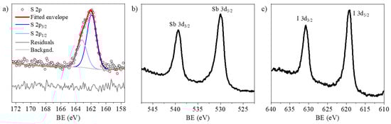
Figure 8.
High resolution XPS spectra of (a) S 2p, (b) Sb 3d and (c) I 3d photoemission regions for the SbSI target.
3.3. Pulsed Electron Deposition of SbSI Thin-Films
Starting from the optimized MC target, SbSI thin films were deposited using the PED technique with an acceleration voltage of 16 kV. The deposition temperature varied between RT and 300 °C, and all samples were deposited on FTO/glass substrates. As demonstrated in Figure 9, the XRD patterns of the films indicate that when the deposition temperature exceeds RT, a phase decomposition occurs, resulting in the sublimation of iodine (I), the partial sublimation of sulfur (S) and the formation of metallic Sb (main reflection detected at 2θ ≈ 28.7°, red curve). At temperatures exceeding 100 °C, the decomposition process gives rise to the formation of highly crystalline Sb and Sb2S3 (blue curve). Consequently, it can be deduced that the preservation of the sample from phase decomposition and the subsequent evaporation of I and S can only be accomplished by depositing SbSI films at RT. However, at ambient temperature, the PED invariably results in the formation of the SbSI amorphous phase (black curve).
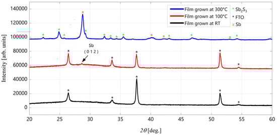
Figure 9.
XRD pattern of SbSI films grown by PED deposited at RT (RT-PED) (black curve), at 100 °C (red curve) and at 300 °C (blue curve).
The Raman spectrum shown in Figure 10 displays a broad distribution of peaks, characteristic of the amorphous nature of the material. Nonetheless, the formation of the SbSI phase is indicated by the close correspondence with the previously reported reference peaks in the 50–200 cm−1 region (for comparison, see Figure 3 and Table 2).
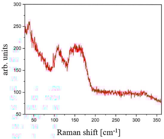
Figure 10.
Raman spectrum of the amorphous SbSI film deposited via RT-PED.
SEM images of SbSI films deposited at RT show a granular structure of the material, which is due to the peculiar morphology of SbSI crystallites (Figure 11a). The thickness of the films, evaluated in cross-section, is approximately 600 nm (Figure 11b). Despite the surface of the film displaying a uniform morphology on a global scale, the presence of micrometric debris has been observed, attributable to the erosion of target pieces.
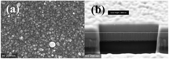
Figure 11.
SEM images of an SbSI film deposited via RT-PED: (a) plan-view image; (b) tilted view of the Focused Ion Beam (FIB) cut cross-section.
To investigate the film composition by EDX, ad hoc samples were deposited on soda–lime glass under the same conditions described above, so as to avoid the interference caused by the overlapping of Sn, attributable to the FTO substrate, and Sb signals. The SbSI films were found to satisfy the stoichiometric ratio close to 1:1:1 across the entirety of the examined surface, within the EDX measurement uncertainty (see Table 3).
The analysis of EDX maps carried out on the deposited films indicates a high level of homogeneity in the composition across the surface. The presence of a small number of micrometric particles on the surface can be attributed to a phase rich in Sb and I (Figure 12).
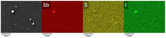
Figure 12.
EDX elemental maps of the SbSI film deposited via RT-PED. The distribution of Sb is shown in red, S in yellow, and I in green.
The optical properties of amorphous SbSI films deposited via PED were investigated using UV-VIS spectrophotometry. The predicted electronic band structure of SbSI is characterized by an indirect forbidden bandgap EgIf = 1.86 eV [37], referred to the transition from the Γ point to the S point of the reciprocal lattice. Standing the various mechanisms of absorption of electromagnetic radiation in semiconductors, which can coexist within the same spectral range, the spectral dependence of the Kubelka-Munk function was fitted with the method proposed by Nowak et al. [38]. Figure 13 illustrates the experimental and calculated Kubelka-Munk function as calculated from the diffuse reflectance spectrum. The fitted band gap values for the as grown films deposited via RT-PED were obtained with high confidence (R2 = 0.9996). The resultant energy bandgap of 1.89 eV, corresponding to a wavelength value of 656 nm, is fully consistent with the theoretical value ascribed to the indirect forbidden transition.
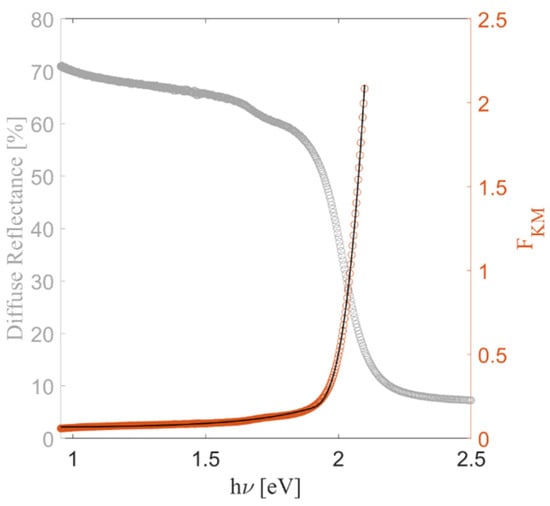
Figure 13.
UV–Vis diffuse reflectance spectrum of the SbSI film deposited via RT-PED, shown on the left axis (gray). The corresponding Kubelka–Munk function is plotted on the right axis (orange), along with the fitting curve (black).
From the perspective of optical properties, the films exhibit significant absorption in the wavelength range of approximately 800 nm. Complete absorption occurs around 300 nm, although a contribution from the glass substrates in the UV region must be considered. These features make the films effective absorbers within the visible spectrum (Figure 14).
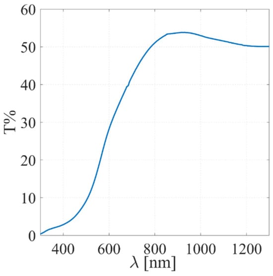
Figure 14.
Measured UV-VIS transmittance of SbSI film deposited via RT-PED.
3.4. Post-Deposition Annealing of SbSI Films
The crystallization of the amorphous room-temperature deposited SbSI films can be induced using post-deposition treatments. Two different post-deposition annealing pathways were evaluated experimentally: (i) the as-grown samples were heated directly in the PED vacuum chamber at 10−1 Pa immediately after RT deposition (vacuum annealing); (ii) the RT-grown samples were extracted from the PED chamber and placed on a hot plate in air (air annealing). For both treatments, the temperature varied up to a maximum of 120 °C and the treatment time was 20 min.
3.4.1. Vacuum Annealing
The best results for vacuum annealing conditions were obtained at 90 °C. At this temperature we observed the formation of an SbSI phase with weak crystallinity, indicated by the appearance of a low peak at ~30°, associated with the main (121) and minor (130), (211) and (310) reflections of SbSI (Figure S3, blue curve). However, although the treatment seems to promote a partial recovering of an ordered structure, it does not cause any major variation in the size and shape of the crystallites, as confirmed by AFM analysis shown in Figure S4. At higher annealing temperatures and durations, sulfur and iodine desorb from the film, resulting in the partial or total decomposition of the SbSI phase (Figure S3, red curve), as it occurs during PED at high temperature.
3.4.2. Air Annealing
XRD patterns in Figure 15 show that air annealing at 90 °C effectively induces the film crystallization, revealing all the reflections of the SbSI phase, including minor peaks such as (220), (310), (040), (320), (330), (141), (002), (150), (241), (411), (341), and (312), with no preferential grain orientation. The resulting degree of crystallinity is comparable to the starting SbSI powders.
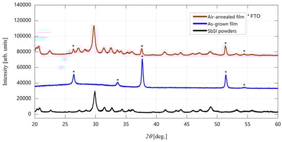
Figure 15.
XRD pattern of the SbSI thin film produced via PED at RT as grown (blue curve) and annealed in air (red curve) at 90 °C for 20 min. The pattern of SbSI powders (black curve) is used as reference.
Interestingly, although the SEM images reveal an overall unaltered morphology (Figure 16), AFM measurements (Figure S4) suggest an increase in both in- and out-of-plane sizes of the SbSI grains following the air-annealing treatment.
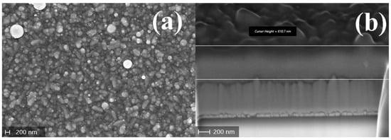
Figure 16.
SEM images of the SbSI film produced via PED at RT and annealed in air at 90 °C for 20 min: (a) plan view and (b) tilted view of the FIB cut cross-section.
Raman analysis in Figure 17 confirms the crystallization of air-annealed films, as evidenced by the narrower peaks, ascribable to the paraelectric phase, that can be distinctly distinguished from the spectrum of the as-grown films. It is worthy of note that a deviation from the powder spectra is apparent, in the form of a shoulder around 166 cm−1. This spectral feature can be attributed to the presence of secondary impurity phases, which is not unexpected given the propensity of the air annealing treatment to promote surface oxidation of the elements.
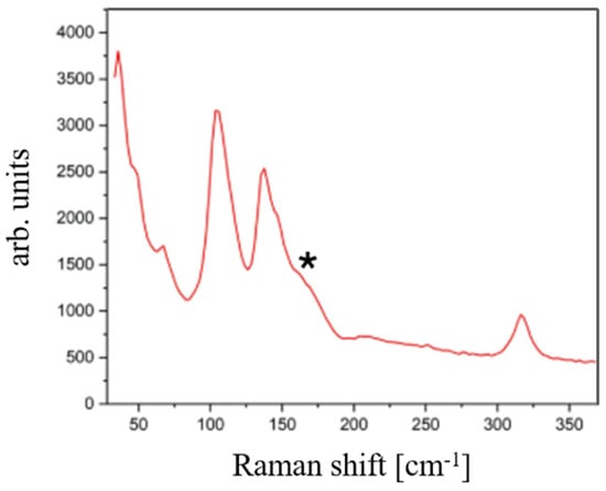
Figure 17.
Raman spectrum of SbSI film after an air-annealing treatment at 90 °C for 20 min. The shoulder (*) appearing at around 166 cm−1 is ascribable to oxide species.
This aspect was further analyzed through XPS analysis (Figure 18), that indicates that air annealing not only promotes crystallization of the SbSI phase but also induces surface decomposition.
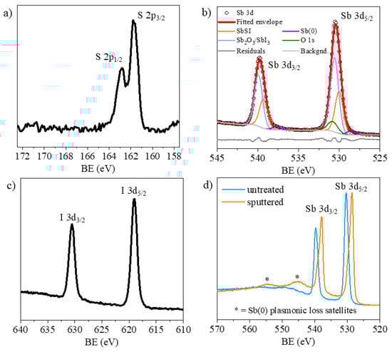
Figure 18.
High resolution XPS spectra of S 2p (a), Sb 3d (b) and I 3d (c) photoemission regions for the air-annealed SbSI thin film. (d) Sb 3d region for the same sample before and after monoatomic Ar+ ion beam sputtering (2000 eV, 60 s).
The surface composition is enriched in Sb (64%) and I (24%) relative to S (12%). The S 2p3/2 peak appears at 161.7 eV, a binding energy typical of sulfide environments, with no evidence of oxidized S species at higher binding energies. Similarly, the I 3d spectrum exhibits a 3d5/2 binding energy of 619.0 eV, characteristic of iodide species. The relative enrichment of Sb and I suggests the presence of decomposition products at the surface. To further investigate these species, the Sb 3d region was analyzed in detail. Peak fitting of Sb 3d requires careful treatment due to the overlap between Sb 3d5/2 and O 1s signals. Accordingly, the Sb 3d5/2 and Sb 3d3/2 peaks were fitted simultaneously, with the 3d3/2 component constraining the spin–orbit doublet. The residual intensity within the Sb 3d5/2 region was attributed to the O 1s contribution. Analysis of the Sb 3d5/2 peak revealed, in addition to the O 1s contribution, two major Sb components: one at 530.0 eV ascribed to SbSI, and another at 530.6 eV assignable to either Sb2O3 or SbI3 [39]. A minor component at 528.5 eV, likely associated with elemental Sb, was also included to improve the fit. The results are summarized in Table 4. The fitting confirms that air annealing causes partial decomposition of the outermost layers. The SbSI component at 530.0 eV accounts for an equimolar amount of sulfur (≈12.5 at.%). Considering the O 1s content (27.4 at.%), the contribution of Sb2O3 is estimated at 18.3 at.%, leaving a smaller fraction (3.9 at.%) attributable to SbI3. This fraction corresponds to 11.8 at.% of iodine deriving from SbI3. After correcting for this contribution, the iodine associated with SbSI is 12.4 at.%. Overall, this analysis confirms that the Sb:S:I stoichiometry of the SbSI phase is preserved at 1:1:1, despite the concurrent formation of Sb2O3, SbI3, and trace amounts of elemental Sb at the surface. Sputtering the surface with a monoatomic Ar+ ion beam progressively reduces the excess of I and Sb. For example, sputtering at 2000 eV for 60 s results in atomic concentrations of Sb 55.4%, I 22.3%, and S 22.3%. After removal of the outermost layers, S and I recover the stoichiometric ratio characteristic of SbSI; however, it should be noted that the sputtering process simultaneously induces a significant reduction in Sb (Figure 18d), even when employing softer conditions such as a cluster ion gun.
Table 4.
XPS Binding energy (BE) and atomic percentages for the SbSI thin film including Sb 3d fitting results.
These findings indicate that the most effective method for synthesizing crystalline and stoichiometric SbSI films is a two-step process. The first step involves the deposition of RT-PED, followed by the second step of annealing in air at temperatures up to 100 °C.
4. Discussion
This study successfully demonstrates a novel and highly effective approach for synthesizing the FE-PV compound SbSI via MC solid-state reaction. By directly reacting elemental antimony, sulfur, and iodine under ambient conditions (without the use of solvents and in the presence of air) this method offers a sustainable and energy-efficient alternative to traditional synthesis routes. The process, performed at RT in a high-energy planetary ball mill with Y:ZrO2 media, was carefully optimized to maximize reaction yield, achieving ideal conditions at 650 rpm, a Ball-to-Powder Ratio of 14, and 20 h duration. The purity and the correct stoichiometric composition of SbSI were verified by PXRD, XPS and EDX techniques, while Raman measurements were found to be useful to unambiguously identify its phase as the paraelectric one, suggesting that MC reaction stabilizes it at T < TC2. These last findings need a more in-depth analysis.
The resulting product is a single-phase orthorhombic SbSI with low crystallinity and heterogeneous morphology, demonstrating the capability of MC synthesis to produce complex ternary compounds from elemental precursors. Subsequent optimization of a two-step sintering process (mechanical compaction followed by prolonged heat treatment at 125 °C) enabled the formation of a dense SbSI target with suitable microstructural and crystallographic properties. This target was effectively employed as a source in a Pulsed Electron Deposition system.
Importantly, the stoichiometric integrity and physical quality of the target enabled high-fidelity transfer during thin-film growth, resulting in uniform SbSI films with an optical band gap of 1.89 eV and remarkable transparency (>50%) in the near-infrared (800–1300 nm) range for a 600 nm thick film. Post-deposition annealing studies revealed that vacuum annealing is counterproductive due to partial phase decomposition and poor crystallization. In contrast, annealing in ambient air at temperatures up to 90 °C promoted polycrystalline film formation while maintaining bulk stoichiometry, albeit with slight surface oxidation. Although an alternative post-deposition annealing under controlled environments and counterpressure is currently being investigated to mitigate the undesired surface oxidation and the sublimation of volatile elements, these results strongly confirm that pulsed electron deposition is a reliable technique for transferring the stoichiometric composition of SbSI from a density-optimized target into a uniform film.
Overall, this study demonstrates that mechanosynthesis is not only a green and scalable approach, but also a powerful route for producing high-purity, stoichiometric compounds such as SbSI. The successful fabrication and use of mechanochemically derived targets for thin-film deposition highlight the potential of this technique for broader application in the deposition of pnictogen chalcohalide films. Furthermore, the methodologies established here can be readily extended to other functional materials, facilitating systematic exploration and optimization of their properties for next-generation electronic and optoelectronic devices.
Supplementary Materials
The following supporting information can be downloaded at: https://www.mdpi.com/article/10.3390/coatings15101232/s1, Figure S1. XRD of the MC SbSI powders for different MC parameters. Figure S2. Rietveld refinement results obtained in Pnam by FullProf [31] using, as starting point, the refined structure model by EXPO. The black, red and blue curves correspond to the calculated, observed and difference patterns, respectively. The calculated 2θ-position of reflections are drawn as green vertical bars. Figure S3. XRD of SbSI films after vacuum annealing treatment at different temperatures: 90 °C (blue curve) and 125 °C (red curve). The main (hkl)-reflections related to SbSI are highlighted (blue curve). Figure S4. AFM images of SbSI films: (a) as-grown, (b) air-annealed at 90 °C and (c) vacuum-annealed at 90 °C. Table S1. SbSI: main results of the Rietveld refinement carried out by EXPO in Pnam (second column) and Pna21 (last column). Table S2. SbSI: the fractional atomic coordinates (x, y, z) of the structure model provided by EXPO at the end of the Rietveld refinement carried out in Pnam (second column) and Pna21 (last column) are given. Refs [30,31,40,41,42,43,44,45,46] are cited in the supplementary materials.
Author Contributions
Conceptualization, D.D., E.D.C., M.C. and S.R.; methodology, D.D., E.D.C., M.C. and S.R.; validation, A.A., E.D.C. and M.C.; formal analysis, A.M., C.G., E.D.C., G.S. and M.R.; investigation, E.D.C., G.S., G.T. and M.C.; resources, D.D. and E.G.; data curation, E.D.C., G.S. and M.C.; writing—original draft preparation, A.M., C.G., E.D.C., M.C. and M.R.; writing—review and editing, A.N., D.C., D.D., E.G., E.A.S.S., F.P., G.T., L.A., M.B., and S.R.; visualization, E.D.C., F.P., G.S., M.C. and S.R.; supervision, D.D., E.G. and S.R.; project administration, D.D. and S.R.; funding acquisition, D.D. and S.R. All authors have read and agreed to the published version of the manuscript.
Funding
This research was funded by Italian Ministry of the Environment and the Energy Security: Research Fund for the Italian Electrical System (type-A call, published on G.U.R.I. n. 192 on 18 August 2022). The research was also funded by Italian Ministry of University and Research: “Ecosystem for Sustainable Transition in Emilia-Romagna” (EcosistER), funded under the National Recovery and Resilience Plan (NRRP), Mission 4 Component 2 Investment 1.5—Call for tender No. 3277 of 30 December 2021.
Institutional Review Board Statement
Not applicable.
Informed Consent Statement
Not applicable.
Data Availability Statement
The original contributions presented in this study are included in the article/Supplementary Materials. Further inquiries can be directed to the corresponding author.
Acknowledgments
This study has been supported by “nuovi Concetti, mAteriali e tecnologie per l’iNtegrazione del fotoVoltAico negli edifici in uno scenario di generazione diffuSa” [CANVAS] project, funded by the Italian Ministry of the Environment and the Energy Security, through the Research Fund for the Italian Electrical System (type-A call, published on G.U.R.I. n. 192 on 18-08-2022). This study was partially developed in the framework of the research activities carried out within the Project “Network 4 Energy Sustainable Transition—NEST”, Spoke 1., Project code PE0000021, funded under the National Recovery and Resilience Plan (PNRR), Mission 4, Component 2, Investment 1.3—Call for tender No. 1561 of 11.10.2022 of Ministero dell’Universita’ e della Ricerca (MUR); funded by the European Union—NextGenerationEU. The ESCALAB QXi spectrometer was funded by the Italian National Research Council via the grant: “Sviluppo delle infrastrutture e programma biennale degli interventi del Consiglio Nazionale delle Ricerche (2019).” A.M. and C.G. gratefully thank F. Baldassarre for his valuable technical help.
Conflicts of Interest
The funders had no role in the design of the study; in the collection, analysis, or interpretation of data; in the writing of the manuscript; or in the decision to publish the results.
Abbreviations
The following abbreviations are used in this manuscript:
| FE-PV | Ferro-Photovoltaic |
| FERAM | Ferroelectric Random-Access Memory |
| MC | Mechanochemistry |
| PED | Pulsed Electron Deposition |
| RPM | Rotational speed |
| BPR | Ball-to-Powder mass ratio |
| FTO | Fluorine-doped Tin Oxide |
| PXRD | Powder X-Ray Diffraction |
| SEM | Scanning Electron Microscopy |
| EDX | Energy-Dispersive X-ray |
| XPS | X-ray Photoelectron Spectroscopy |
| AFM | Atomic Force Microscopy |
| RT | Room temperature |
References
- Aguiar, I.; Mombrú, M.; Pérez Barthaburu, M.; Bentos Pereira, H.; Fornaro, L. Influence of solvothermal synthesis conditions in BiSI nanostructures for application in ionizing radiation detectors. Mater. Res. Express 2016, 3, 025012. [Google Scholar] [CrossRef]
- Limin, S.; Shujuan, Z.; Qingwu, W. Porous BiOI Sonocatalysts: Hydrothermal Synthesis, Characterization, Sonocatalytic, and Kinetic. Ind. Eng. Chem. Res. 2012, 51, 1193–1197. [Google Scholar] [CrossRef]
- Kijima, N.; Matano, K.; Saito, M.; Oikawa, T.; Konishi, T.; Yasuda, H.; Sato, T.; Yoshimura, Y. Oxidative catalytic cracking of n-butane to lower alkenes over layered BiOCl catalyst. Appl. Catal. A Gen. 2001, 206, 237–244. [Google Scholar] [CrossRef]
- Li, X.-H.; Shi, Z.-H.; Yang, M.; Liu, W.; Guo, S.-P. Sn7Br10S2: The First Ternary Halogen-Rich Chalcohalide Exhibiting a Chiral Structure and Pronounced Nonlinear Optical Properties. Angew. Chem. Int. Ed. 2022, 61, e202115871. [Google Scholar] [CrossRef] [PubMed]
- Fong, C.Y.; Wooten, F. Experimental and Theoretical Study of the Feasibility of the Gunn Effect in BiSCl, BiSBr, BiSI, BiSeI, BiSeBr and BiSeCl; The Department of Applied Science, University of California: Davis, CA, USA, 1981; AFOSR-TR-81-0452. [Google Scholar] [CrossRef]
- Starczewska, A. New approach to well-known compounds: Fabrication and characterization of AVBVICVII nanomaterials. Acta Phys. Pol. A 2021, 139, 394–400. [Google Scholar] [CrossRef]
- Audzijonis, A.; Sereika, R.; Žaltauskas, R. Antiferroelectric phase transition in SbSI and SbSeI crystals. Solid State Commun. 2008, 147, 88–89. [Google Scholar] [CrossRef]
- Zhang, Y.; Mao, J.; Zheng, R.-K.; Zhang, J.; Wu, Y.; Wang, X.; Miao, K.; Yao, H.; Yang, L.; Zheng, H. Ferroelectric Polarization-Enhanced Performance of Flexible CuInP2S6 Piezoelectric Nanogenerator for Biomechanical Energy Harvesting and Voice Recognition Applications. Adv. Funct. Mater. 2023, 33, 2214745. [Google Scholar] [CrossRef]
- Xu, T.; Switkowski, K.; Chen, X.; Liu, S.; Koynov, K.; Yu, H.; Zhang, H.; Wang, J.; Sheng, Y.; Krolikowski, W. Three-dimensional nonlinear photonic crystal in ferroelectric barium calcium titanate. Nat. Phot. 2018, 12, 591–595. [Google Scholar] [CrossRef]
- Huang, Q.; Ma, C.; Wang, N.; Zhang, H.; Lee, C.; Ma, Y. Photodetectors based on two-dimensional materials/ferroelectrics hybrid system: Physics, structures, and applications. Mater. Sci. Eng. R Rep. 2025, 164, 100986. [Google Scholar] [CrossRef]
- Pan, J.; Wang, Z.; Zhao, B.; Yin, J.; Guo, P.; Yang, Y.; Ren, T.-L. Recent Progress of Non-Volatile Memory Devices Based on Two-Dimensional Materials. Chips 2024, 3, 271–295. [Google Scholar] [CrossRef]
- Mistewicz, K.; Nowak, M.; Stróż, D. A Ferroelectric-Photovoltaic Effect in SbSI Nanowires. Nanomaterials 2019, 9, 580. [Google Scholar] [CrossRef]
- Caño, I.; Navarro-Güell, A.; Maggi, E.; Gon Medaille, A.; Rovira, D.; Jimenez-Arguijo, A.; Segura, O.; Torrens, A.; Jimenez, M.; López, C.; et al. Ribbons of Light: Emerging (Sb,Bi)(S,Se)(Br,I) Van der Waals Chalcohalides for Next-Generation Energy Applications. Small 2025, 21, e05430. [Google Scholar] [CrossRef] [PubMed]
- Yang, S.Y.; Seidel, J.; Byrnes, S.J.; Shafer, P.; Yang, C.H.; Rossell, M.D.; Yu, P.; Chu, Y.H.; Scott, J.F.; Ager, J.W., 3rd; et al. Above-bandgap voltages from ferroelectric photovoltaic devices. Nat. Nanotechnol. 2010, 5, 143–147. [Google Scholar] [CrossRef] [PubMed]
- Zenkevich, A.; Matveyev, Y.; Maksimova, K.; Gaynutdinov, R.; Tolstikhina, A.; Fridkin, V. Giant bulk photovoltaic effect in thin ferroelectric BaTiO3 films. Phys. Rev. B 2014, 90, 161409. [Google Scholar] [CrossRef]
- Ichiki, M.; Maeda, R.; Morikawa, Y.; Mabune, Y.; Nakada, T.; Nonaka, K. Photovoltaic effect of lead lanthanum zirconate titanate in a layered film structure design. Appl. Phys. Lett. 2004, 84, 395–397. [Google Scholar] [CrossRef]
- Han, X.; Ji, Y.; Yang, Y. Ferroelectric photovoltaic materials and devices. Adv. Funct. Mater. 2022, 32, 2109625. [Google Scholar] [CrossRef]
- Fatuzzo, E.; Harbeke, G.; Merz, W.J.; Nitsche, R.; Roetschi, H.; Ruppel, W. Ferroelectricity in SbSI. Phys. Rev. 1962, 127, 2036–2037. [Google Scholar] [CrossRef]
- Wang, Y.; Hu, Y.; Chen, Z.; Guo, Y.; Wang, D.; Wertz, E.A.; Shi, J. Effect of strain on the Curie temperature and band structure of low-dimensional SbSI. Appl. Phys. Lett. 2018, 112, 183104. [Google Scholar] [CrossRef]
- Kern, R. An electro-optical and electromechanical effect in SbSI. J. Phys. Chem. Solids 1962, 23, 249–253. [Google Scholar] [CrossRef]
- Ibanez, A.; Jumas, J.-C.; Olivier-Fourcade, J.; Philippot, E.; Maurin, M. Sur les chalcogeno-iodures d’antimoine SbXI(X = S, Se, Te): Structures et spectroscopie Mo¨ssbauer de121Sb. J. Solid State Chem. 1983, 48, 272–283. [Google Scholar] [CrossRef]
- Su, X.; Liu, Y.; Xiao, C.; Zhang, G.; Liu, T.; Qin, J.; Chen, C. A facile, clean and quantitative synthesis of antimony chloride oxide single crystals. Mat. Lett. 2006, 60, 3879–3881. [Google Scholar] [CrossRef]
- Dubey, H.K.; Deshmukh, L.P.; Kshirsagar, D.E.; Sharon, M.; Sharon, M. A study of the electrical properties of SbSI synthesized using CVD techniques. QScience Connect 2013, 2013, 40. [Google Scholar] [CrossRef]
- Szperlich, P.; Toroń, B.; Nowak, M.; Jesionek, M.L.; Kępińska, M.; Bogdanowicz, W. Growth of large SbSI crystals. Mater. Sci.-Pol. 2014, 32, 669–675. [Google Scholar] [CrossRef]
- Delmonte, D.; Manfredi, R.; Calestani, D.; Mezzadri, F.; Righi, L.; Mazzer, M.; Pattini, F.; Rampino, S.; Spaggiari, G.; Gilioli, E. An affordable method to produce CuInS2 ‘mechano-targets’ for film deposition Semicond. Sci. Technol. 2020, 35, 045026. [Google Scholar] [CrossRef]
- Casappa, M.; Pattini, F.; Spaggiari, G.; Mezzadri, F.; Rampino, S. Growth of multiferroic γ-BaFe2O4 thin films by Pulsed Electron Deposition technique. J. Alloys Compd. 2024, 987, 174193. [Google Scholar] [CrossRef]
- Spaggiari, G.; Bersani, D.; Calestani, D.; Gilioli, E.; Gombia, E.; Mezzadri, F.; Casappa, M.; Pattini, F.; Trevisi, G.; Rampino, S. Exploring Cu-Doping for Performance Improvement in Sb2Se3 Photovoltaic Solar Cells. Int. J. Mol. Sci. 2022, 23, 15529. [Google Scholar] [CrossRef]
- Stancari, F.; Rampino, S.; Pattini, F.; Mezzadri, F.; Spaggiari, G.; Parisini, A.; Pavesi, M.; Baraldi, A.; Rancan, M.; Armelao, L.; et al. Tetravalent element doping of β-Ga2O3 films grown by Pulsed Electron Deposition technique. J. Alloys Compd. 2025, 1027, 180581. [Google Scholar] [CrossRef]
- Kikuchi, A.; Oka, Y.; Sawaguchi, E. Crystal structure determination of SbSI. J. Phys. Soc. Jpn. 1967, 23, 337–354. [Google Scholar] [CrossRef]
- Altomare, A.; Cuocci, C.; Giacovazzo, C.; Moliterni, A.; Rizzi, R.; Corriero, N.; Falcicchio, A. EXPO2013: A kit of tools for phasing crystal structures from powder data. J. Appl. Cryst. 2013, 46, 1231–1235. [Google Scholar] [CrossRef]
- Rodríguez-Carvajal, J. Recent advances in magnetic structure determination by neutron powder diffraction. Phys. B Condens. Matter 1993, 192, 55–69. [Google Scholar] [CrossRef]
- Balkanski, M.; Teng, M.K.; Shapiro, S.M.; Ziolkiewicz, M. Lattice modes and phase transition in SbSI. Phys. Stat. Sol. 1971, 44, 355–368. [Google Scholar] [CrossRef]
- Özer, T. Investigation of pressure dependence of mechanical properties of SbSI compound in paraelectric phase by Ab Initio method. Comput. Condens. Matter 2021, 28, e00568. [Google Scholar] [CrossRef]
- Grigas, J.; Talik, E.; Lazauskas, V. Splitting of the XPS in Ferroelectric SbSI crystals. Ferroelectrics 2003, 284, 147–160. [Google Scholar] [CrossRef]
- Grigas, J.; Talik, E.; Lazauskas, V. X-ray photoelectron spectroscopy of ferroelectric semiconductor SbSI crystals. Lith. J. Phys. 2004, 44, 427–438. [Google Scholar] [CrossRef]
- Ikemoto, I. X-ray photoelectron spectroscopic studies of SbSI. Bull. Chem. Soc. Jpn. 1981, 54, 2519–2520. [Google Scholar] [CrossRef]
- Yuan, Y.; Xiao, Z.; Yang, B.; Huang, J. Arising applications of ferroelectric materials in photovoltaic devices. J. Mater. Chem. A 2014, 2, 6027–6041. [Google Scholar] [CrossRef]
- Nowak, M.; Kauch, B.; Szperlich, P. Determination of energy band gap of nanocrystalline SbSI using diffuse reflectance spectroscopy. Rev. Sci. Instrum. 2009, 80, 046107. [Google Scholar] [CrossRef]
- NIST X-Ray Photoelectron Spectroscopy Database, Version 5.0 (Last Update 2023). Available online: https://doi.org/10.18434/T4T88K (accessed on 18 April 2025).
- Altomare, A.; Campi, G.; Cuocci, C.; Eriksson, L.; Giacovazzo, C.; Moliterni, A.; Rizzi, R.; Werner, P.-E. Advances in Powder Diffraction Pattern Indexing: N-TREOR09. J. Appl. Cryst. 2009, 42, 768–775. [Google Scholar] [CrossRef]
- De Wolff, P.M. A Simplified Criterion for the Reliability of a Powder Pattern Indexing. J. Appl. Cryst. 1968, 1, 108–113. [Google Scholar] [CrossRef]
- Altomare, A.; Camalli, M.; Cuocci, C.; Giacovazzo, C.; Moliterni, A.G.G.; Rizzi, R. Advances in Space-Group Determination from Powder Diffraction Data. J. Appl. Cryst. 2007, 40, 743–748. [Google Scholar] [CrossRef]
- Altomare, A.; Caliandro, R.; Camalli, M.; Cuocci, C.; Da Silva, I.; Giacovazzo, C.; Moliterni, A.G.G.; Spagna, R. Space-Group Determination from Powder Diffraction Data: A Probabilistic Approach. J. Appl. Cryst. 2004, 37, 957–966. [Google Scholar] [CrossRef]
- Le Bail, A.; Duroy, H.; Fourquet, J.L. Ab-Initio Structure Determination of LiSbWO6 by X-Ray Powder Diffraction. Mat. Res. Bull. 1988, 23, 447–452. [Google Scholar] [CrossRef]
- Giacovazzo, C. Phasing in Crystallography—A Modern Perspective; International Union of Crystallography/Oxford University Press: Chester, UK, 2013; ISBN 9780199686995. [Google Scholar]
- Rietveld, H.M. A profile refinement method for nuclear and magnetic structures. J. Appl. Cryst. 1969, 2, 65–71. [Google Scholar] [CrossRef]
Disclaimer/Publisher’s Note: The statements, opinions and data contained in all publications are solely those of the individual author(s) and contributor(s) and not of MDPI and/or the editor(s). MDPI and/or the editor(s) disclaim responsibility for any injury to people or property resulting from any ideas, methods, instructions or products referred to in the content. |
© 2025 by the authors. Licensee MDPI, Basel, Switzerland. This article is an open access article distributed under the terms and conditions of the Creative Commons Attribution (CC BY) license (https://creativecommons.org/licenses/by/4.0/).