Abstract
A revisited study of perovskite-based manganite La0.67Sr0.33MnO3 (LSMO) deposited onto corning-glass (CG) substrates is reported here. The LSMO films were fabricated with RF sputtering with different deposition times, varying from 60 to 180 min, resulting in films with thicknesses of 35.0–109.7 nm. Rietveld refinements of the XRD spectrum showed that the samples exhibited hexagonal structures with a space group of R-3c (167) and remained unmodified structures. Clusters of monolayer growth were observed from the morphologies of the films. Interestingly, the average particle size obtained with an AFM perceived an insignificant variation of 31.7–35.6 nm despite the film thickness increment. Optical, electrical and magnetic properties were studied, as particle-size variation usually has a notable contribution to changes in these properties. It was found that the optical band gap (Eg) was in direct variation with the deposition time due to enhanced thickness and surface roughness. The temperature dependence of the resistivity graph was fitted with the percolation model to obtain further enlightenment on the electrical transport in the films. Low-field magnetoresistance (LFMR) was observed for all samples. Ferromagnetic to paramagnetic transition was observed in the vicinity of all samples’ TC values.
1. Introduction
In light of the discovery of colossal magnetoresistance (CMR), low-field magnetoresistance (LFMR), the double exchange (DE) mechanism, ferrometallic and parainsulating transition behaviour and promising applications in microelectronic and optoelectronic devices, meticulous studies have been conducted on the perovskite-structured rare-earth-based manganite R1−xAxMnO3 (R = trivalent rare earth and A = divalent alkali earth) [1,2,3,4]. Particularly captivating are the nanostructures of these oxides’ thin films for their finite size and the significant ratio of surface-to-volume contribution to their unique features. One of the most intriguing materials for devices operating at room temperature (RT) is the lanthanum strontium manganite La1−xSrxMnO3 (LSMO), with a Curie temperature (TC) of about 370 K when doped with the ideal Sr concentration of x = 0.33 [5]. Over recent decades, LSMO has not yet been fully integrated as a source of spin-polarised carriers in device application, despite the fact that its theoretical applicability is of utmost significance. In conjunction with optimization and application of LSMO, the crystal structure, lattice constant, crystal plane orientation and other characteristics of the preselected substrate are known to have a significant impact on the lattice strain of thin films and their magnetic properties [6,7,8]. In addition, it has been well-established in the literature that parameters such as film thickness, lattice strain, annealing conditions and others have a significant impact on manganite thin films’ optical, magnetic and electrical transport properties [9,10,11].
In agreement with expanding the research horizons of LSMO film-fabrication optimization, researchers have been reporting studies from varying aspects, as mentioned earlier. Earlier research on ultrathin (110) oriented LSMO films produced on SrTiO3 (110) substrates showed a strain-induced RT insulating magnetic phase with a FM structure with a TC of about 330 K for thicknesses above 15-unit cells [12]. Epitaxial LSMO/MgO films with TM-I and TC at 406 K confirmed correlation of electrical and magnetic properties [13]. Ramirez Camacho et al. reported decent-quality LSMO films prepared on SiOx/Si (100) substrates in the superparamagnetic state for thicknesses of 40 and 60 nm [14]. Recently, a promising nanostructured LSMO polycrystalline film grown on quartz with greater LFMR (31%), CMR (56%) and sensitivity (0.28 V/T at B = 0.25 T) was fabricated and suggested by Stankevic et al. for CMR sensors [2]. Bojun et al. reported the fabrication of PSMO films, growing on SrTiO3 films, with the potential for magnetic refrigeration application [15]. However, such studies with LSMO deposition on corning glass (CG) were halted after 2014 due to their amorphous natures [7,16,17]. Hence, in consideration of investigating possibilities of further enhancement, a revisited study of preparing polycrystalline LSMO/CG is carried out and reported here.
2. Materials and Methods
LSMO films were fabricated on corning-glass (CG) substrates via RF sputtering (Kurt J. Lesher PVD-75, Jefferson Hills, Allegheny County, PA, USA) using a La0.67Sr0.33MnO3 target (99.9%, Semiconductor Wafer Inc, Taiwan). The CG substrates were ultrasonically cleaned with distilled water, acetone and methanol before deposition. The deposition was carried out at room temperature via applying an RF power of 150 W, with the deposition time ranging from 60 min to 180 min. Hence, the samples are denoted as T6, T9, T12, T15 and T18 in further discussion. Argon and oxygen gases of 99.9% purity were flowed, with a ratio of 80:20, throughout the deposition. The prepared films were postannealed at 700 °C for 2 h in the furnace under ambient conditions.
A structural characterisation was performed with an X-ray diffractometer (XRD, Philips PW 3040/60 X’Pert Pro, Malvern Panalytical, Malvern, UK) with Cu Kα radiation and the specification of 2θ scan (25 min) with omega = 2°, and the range of 2θ was 20°–80°. Rietveld analysis was performed on the XRD patterns using HighScore Plus 3.0 software. Surface morphologies were observed and measured with an atomic force microscope (AFM, Bruker Dimension Edge) in contact mode on a selected region of 1 μm × 1 μm. The AFM images were analysed using NanoScope Analysis 1.7. The thicknesses of the samples were measured with Schottky field emission scanning electron microscopy (FESEM, SU5000, Hitachi, UK). Electrical properties were analysed with a Hall-effect measurement system (HMS, Lakeshore 7604, Lake Shore Cryotronics, Westerviller, OH, USA) in the temperature range of 80–300 K. A vibrating sample magnetometer (VSM, Lakeshore 7407, Lake Shore Cryotronics, Westerviller, OH, USA) was utilised to study the magnetic properties of the samples in the temperature range of 100–420 K. The UV-Vis absorption optical spectra of all samples were measured in the range of 220–2600 nm with a UV-Vis-NIR spectrophotometer (UV3600, Shimadzu, Kyoto, Japan), using CG as a reference.
3. Results and Discussion
The X-ray diffraction patterns of the as-deposited and postannealed LSMO thin films are presented in Figure 1a. The as-prepared sample (T18) was in an amorphous form, and all postannealed samples displayed full crystallization in a single phase towards the (104) direction. The patterns were indexed with a hexagonal lattice (ICSD reference code: 98-010-7027) with an R-3c (167) space group. The rise of peak intensity from T6 to T18 justified the enhancement of film crystallinity with the deposition time. All XRD patterns were Rietveld-refined to obtain the structural parameters, as tabulated in Table 1. The calculations and experiments well fitted as indicated from the small values of the residuals for weighted pattern RWP, pattern RP and χ2. These parameters are congruous with the literature values for La0.67Sr0.33MnO3: of a = 5.469 Å and c = 13.42 Å at 300 K [18]. The bond angle and bond distance remained intact despite deposition-time variation, elucidating that the double exchange (DE) interaction was not disturbed through the series. The value of the average crystallite size, D, was calculated from the peak with the highest intensity, using Scherrer’s equation [19]:
where K is the grain shape factor (=0.90), λ is the wavelength of Cu Kα radiation (=1.5406 Å), β represents the full width at half maximum (FWHM) for which β = βsample − βinstrumental and θ corresponds to the Bragg angle. The peak broadening of all samples was almost negligible, which correlates with the insignificant change in the crystallite size of all LSMO samples tabulated in Table 2. From the consistency of the FWHMs and crystallite sizes throughout the series, we interpreted that the lattice strain is independent of deposition time.
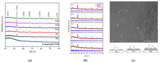
Figure 1.
(a) XRD patterns of all indexed peaks, (b) Rietveld refinement of the XRD patterns of LSMO thin films with varied deposition times and (c) typical FESEM micrograph of the film surface and the suggested growth mechanism.

Table 1.
Rietveld refinement data of LSMO thin films with varied deposition times.
Table 2.
FWHMs, crystallite sizes, particle sizes, average thicknesses, surface roughnesses, TM-I values and TC values of LSMO thin films with varied deposition times.
The representative surface micrograph of LSMO thin film on the CG substrate was obtained with FESEM, as shown in Figure 1b, and the cross-sectional images (not shown) were analysed to attain the average thickness, as presented in Table 1. Figure 1b depicts the suggested crystal growth, which begins with discrete-island nucleation and growth, forming a monolayer island of the deposit. The monolayers eventually merge to create a continuous monolayer of the deposit [20]. Hence, in repetition, this causes the deposit to increase, layer upon layer, forming monolayer clusters.
Numerous variables, including particle size, film thickness and surface roughness, are conjectured to be in correlation with the materials’ optical properties [21,22]. On that account, the crystal structure growth of LSMO film over the CG substrate was analysed, and the AFM micrographs are exemplified in Figure 2a–e. The flatter technique was used before any statistical analysis of the scanned images to assure that only the changes in the heights inherent to the surface were taken into consideration [23]. The surface roughness was characterized via taking the root-mean-square roughness, which represents the deviance of the average height from the crystallite mean height [24]. The particle size was also measured from the AFM images and is compiled in Table 2, with surface roughnesses of T6 to T18. Along with the progression of deposition times, the film thicknesses and the surface roughnesses increased while the particle sizes were kept invariable.
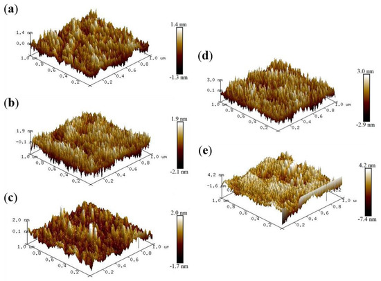
Figure 2.
AFM micrographs of (a) T6, (b) T9, (c) T12, (d) T15 and (e) T18 thin films.
Ultraviolet-visible absorption spectroscopy for T6 to T18 was obtained and analysed via employing Tauc’s relation [22,25,26]:
with α representing the absorption factor (α = 2.302 (A/d)), hv denoting the photon energy and Eg denoting the optical band gap. The value of n is an index that depends on the type of electron transition that induces absorption, given values of n = ½ (indirect) or 2 (direct). The observation of a linear relationship between (αhv)2 and hv suggested a direct transition process occurring in the current system. The intercepts of the extrapolation of the linear region (red dashed line) to the x–axis marked the Eg values, as shown in Figure 3. The quantified Eg values for T6 to T18 ranged from 3.205 eV to 3.450 eV, which is greater than the published value for the LSMO of 2 eV [27]. This is addressed with the occurrence of the quantum confinement effect, where particle-size reduction induces a broadening of the energy level distance between the valence band maximum to the conduction band minimum [28]. These observed band gaps fall into the category of wide-band-gap semiconductors. Interestingly, the Eg values were in gradual increments despite the particle-size consistency. Hence, this led to the implication of film-thickness and surface-roughness contribution to the Eg values. Considering that a nanoscaled film allows complete light penetration, the augmentation of the gap with film thickness and surface roughness allowed us to conjecture more penetration of light into the films with more atomic layers; hence, more light is absorbed. On the other hand, the previous literature suggested that film thickness progression reduces its imaginary refractive index due to thicker layer formation and disappearance of cavities, which leads to higher Eg values [9].
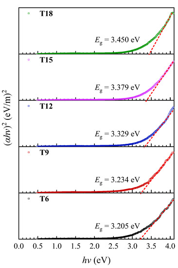
Figure 3.
Tauc plot of LSMO thin films with varied deposition times.
As known, DE interaction is the transfer of electrons from one manganese ion to an adjacent manganese ion via an oxygen ion (Mn3+-O2−-Mn4+), which also gives rise to magnetic coupling between the manganese ions [29]. The manganese spins require parallelism prior to the electrons’ transportation in order to induce charge movement, hence contributing to the magnetic behaviour of perovskite-structured monovalent or divalent ion-doped manganese oxides [30]. Temperature dependencies of in-plane magnetization (M-T) in the range of 100–240 K were measured using the application of a 200 Oe magnetic field with zero-field-cooled (ZFC) conditions. With the corresponding measurements, they were found in the ferromagnetism–paramagnetism transition at its Curie temperature (TC), as represented in Figure 4. The derivative of M (dM/dT) over the T curve (not shown) provided the value of the TC at the turning point of the curve, as shown in Table 2. The recorded TC values, ranging from 338 K to 345 K, are slightly lower compared to the bulk (TC = 370 K [31]). Variation of film thickness contributes to different structural disorders and defects. Thinner films with less completion of monolayers lead to domain-wall pinning, which decreases domain-wall movements. This enhances magnetic viscosity (reduction in domain-activation volume), leading to a lower TC. In addition, the TC was found to be in the vicinity of each transition despite the variation of deposited time due to trivial particle-size differences. Smaller particle size (compared to its bulk) leads to a greater surface-to-volume ratio, which contributes to lesser long-range ferromagnetic order. This contributes to the wide-phase ferromagnetism–paramagnetism transition. Hence, for the films, we comprehended a larger surface-spin portion of weaker magnetic coupling, with the antiferromagnetic phase being restrained [32]. Furthermore, Figure 4a illustrates a graph of the M values as a function of the applied magnetic field (M-H), characterized at room temperature (300 K) with H = ±50 kOe. Hysteresis loops were amended via deducting the diamagnetic response from the CG. Typical FM hysteresis loops with magnetic saturation were obtained, as shown in Figure 4b. Moreover, all of the films showed nearly linear M-H graphs at 400 K (not shown), reflecting paramagnetic properties.
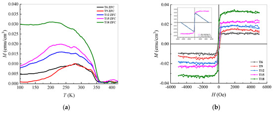
Figure 4.
(a) M-T and (b) M-H at 300 K for LSMO thin films with varied deposition times.
The resistivity of LSMO thin films with distinct deposition times was analysed in the 80–300 K temperature range. It was then plotted as a function of temperature, ρ(T), for further analysis, as shown (open symbols) in Figure 5. The resistivity escalated over rising temperature and started to deplete after a robust peak. This phenomenon originates from metallic behaviour due to double-exchange (DE) interaction and later from semiconducting/insulating behaviour due to Jahn–Teller distortion [29]. Hence, the point of inflexion (arrow) in Figure 5 is taken as the transition temperature of metallic and insulating behaviour (TM-I). The films’ resistivities and the deposition times were in inverse variation. At lower temperatures, where T < TM-I, the metallic phase resistivity plot was quantitatively approximated to an expression inclusive of multiple scattering mechanisms [33,34]:
where ρr1 is designated as the remaining resistivity contributed from the grain boundaries and internal defects, ρ2 is electron–electron interactions and ρ4.5 denotes the scattering process of two magnons. On the other hand, at higher temperatures, where T > TM-I, the semiconducting/insulating resistivity plot was represented with the adiabatic small-polaron-hopping (SPH) model [34,35]:
in which ρr, EA and kB stand for the remaining resistivity, polaron-hopping activation energy and Boltzmann’s constant, respectively. Taking into consideration the percolation approach (around the transition peak) and the coexistence of metallic conductivity in the FM region with semiconductivity in the PM region, the resistivity over the whole temperature range is written as [35,36]:
with fv representing the volume fraction of metallic clusters that complies with Boltzmann’s distribution:
where
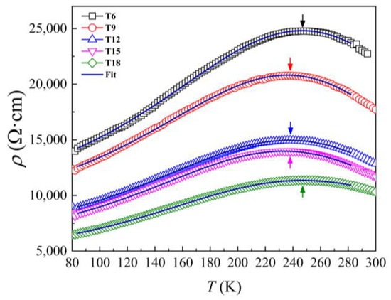
Figure 5.
Graph of resistivity as a function of temperature of LSMO thin films with varied deposition times.
Here, the energy disparity between FM and PM is referred to as ∆U, and a temperature that is close to the point when the resistivity maximizes is written as (usually equal/near to TC). Hence,
The following conditions can be deduced based on Equation (6) [37]:
- (i)
- , (sample is semiconducting/insulating);
- (ii)
- , (sample is metallically governed);
- (iii)
- , .
Figure 5 shows the best percolation fit line (dark blue solid line), in the ρ(T) graph of prepared LSMO thin films, to Equation (8b) at H = 0 kOe, and the obtained parameters are presented in Table 3. Assurance of excellent fitting was given with the evaluation of the R2 value, which approached one.
Table 3.
Percolation-fit parameters obtained for LSMO thin films with varied deposition times.
The fitting parameter ρr1 demonstrated the greatest significance out of all the parameters. The noticeable reduction in resistivity magnitude over the film’s deposition time can be justified with the grain or domain-boundary effect. Typical grain or domain-boundary effect reduction is attributed to density of effective grain boundaries [38], which does not hold in our scenario, since our films had almost identical particle sizes. Instead, this can be ascribed to another factor, of better grain connectivity in the thicker films, due to greater atomic-layer growth on CG from longer deposition times. This distinction of U0 may be addressed with the significant contribution of the grain boundary, which reduces the DE and, as a result, renders the film less conductive from T18 to T6.
Figure 6 demonstrates the applied magnetic field; H represents dependencies of magnetoresistance and MR (%) represents the graph of the series utilizing the equation
with ρ0 and ρH, respectively, denoting the resistivities before and after the applied magnetic field. The MR graph exhibits two distinguishable parts, a steeper (H ≤ 2 kOe) descent followed by a more gradual (H ≥ 2 kOe) descent, known as extrinsic MR (or LFMR) and intrinsic MR, with the progression of the applied magnetic field. Extrinsic MR is contributed through a vital drop of resistance as a consequence of the spin-polarised tunnelling effect [39]. This is due to enhancement of hopping of eg electrons as randomly oriented spins in manganite grains are aligned towards the direction of a low magnetic field [40]. On the other hand, in intrinsic MR, which has higher H, the spins in the grains’ cores are further aligned, which promotes a gentle reduction in resistance. The greatest LFMR, of −9.483% (H = 2 kOe), and MR, of −13.285% (H = 10 kOe) at 80 K, were reported for the T15 sample.
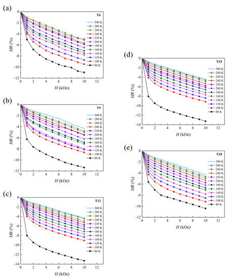
Figure 6.
Applied magnetic field dependencies of MR from 80 to 300 K for LSMO thin films with varied deposition times. (a) T6; (b) T9; (c) T12; (d) T15; (e) T18.
4. Conclusions
Polycrystalline La0.67Sr0.33MnO3 thin films were successfully deposited on corning-glass substrates via RF sputtering with controlled deposition times. In contrast to any earlier study on thickness-dependent particle size in LSMO films fabricated via other methods, our study suggested an insignificant change in particle size, of 31.7–35.6 nm, with a change in thickness from 35.0 nm to 109.7 nm. In spite of similar particle sizes over the series, the electrical resistivity reduced from T6 to T18, with comparable TM-I. Longer deposition times led to thicker films with higher surface roughnesses due to a greater amount of atomic layers, contributing to more light absorption; hence, the optical band gap rose (Eg). T15 showcased the greatest LFMR, of −9.483% (H = 2 kOe), and MR, of −13.285% (H = 10 kOe), at 80 K. Magnetic saturation was achieved along with typical FM hysteresis loops at 300 K. Additionally, at 400 K, the samples all exhibit almost linear M-H graphs, which represent paramagnetic characteristics.
Author Contributions
Conceptualization, Y.J.W., L.N.L. and K.P.L.; methodology, Y.J.W., L.N.L., N.A.A.D. and K.P.L.; validation, Y.J.W., L.N.L., X.T.H. and N.A.A.D.; formal analysis, Y.J.W., L.N.L., X.T.H. and N.A.A.D.; investigation, Y.J.W., L.N.L., X.T.H. and N.A.A.D.; resources, K.P.L., M.M.A.K., S.K.C., M.K.B.S., M.M. and A.H.S.; writing—original draft preparation, Y.J.W.; writing—review and editing, Y.J.W., L.N.L. and K.P.L.; visualization, Y.J.W., L.N.L. and K.P.L.; supervision, K.P.L., M.M.A.K., S.K.C., M.K.B.S., A.H.S. and M.M.; project administration, K.P.L., M.M.A.K., S.K.C., M.K.B.S. and A.H.S.; funding acquisition, K.P.L., M.M.A.K., S.K.C., M.K.B.S. and A.H.S. All authors have read and agreed to the published version of the manuscript.
Funding
This research was fully financed and supported by the Ministry of Higher Education, Malaysia (MOHE), through the Fundamental Research Grant Scheme (FRGS/1/2019/STG07/UPM/02/4).
Institutional Review Board Statement
Not applicable.
Informed Consent Statement
Not applicable.
Data Availability Statement
The data presented in this study are available on request from the corresponding authors.
Acknowledgments
This paper was partly supported by Japan Science and Technology (JST) for advanced Project Based Learning (aPBL), Shibaura Institute of Technology (SIT), under the Top Global University Project designed by the Ministry of Education, Culture, Sports, and Science & Technology, Japan.
Conflicts of Interest
The authors declare no conflict of interest.
References
- Dagotto, E.; Hotta, T.; Moreo, A. Colossal magnetoresistant materials: The key role of phase separation. Phys. Rep. 2001, 344, 1–153. [Google Scholar] [CrossRef]
- Stankevic, V.; Zurauskiene, N.; Kersulis, S.; Plausinaitiene, V.; Lukose, R.; Klimantavicius, J.; Tolvaisiene, S.; Skapas, M.; Selskis, A.; Balevicius, S. Nanostructured Manganite Films Grown by Pulsed Injection MOCVD: Tuning Low- and High-Field Magnetoresistive Properties for Sensors Applications. Sensors 2022, 22, 605. [Google Scholar] [CrossRef]
- Majumdar, S.; Dijken, S.v. Pulsed laser deposition of La1−xSrxMnO3: Thin-film properties and spintronic applications. J. Phys. D Appl. Phys. 2014, 47, 034010. [Google Scholar] [CrossRef]
- Boora, N.; Rani, P.; Nagal, V.; Rahman, S.; Awana, V.S.; Hafiz, A. Synthesis, characterization of LCMO composite and fabrication of its thin films by RF magnetron sputtering for room-temperature applications. AIP Conf. Proc. 2020, 2276, 020047. [Google Scholar]
- Yamada, Y.; So, J.; Asano, H.; Tazawa, M.; Yoshimura, K. Temperature dependence of optical constants of La0.7Sr0.3MnO3 thin films. Appl. Surf. Sci. 2017, 421, 866–869. [Google Scholar] [CrossRef]
- El Helali, S.; Daoudi, K.; Boudard, M.; Schulman, A.; Acha, C.; Roussel, H.; Oumezzine, M.; Oueslati, M. Strain dependence of the physical properties of epitaxial La0.7Ca0.3MnO3 thin films grown on LaAlO3 substrates. J. Alloys Compd. 2016, 655, 327–335. [Google Scholar] [CrossRef]
- Navasery, M.; Halim, S.A.; Dehzangi, A.; Soltani, N.; Bahmanrokh, G.; Erfani, H.M.; Kamalianfar, A.; Pan, K.Y.; Chang, S.C.; Chen, S.K.; et al. Electrical properties and conduction mechanisms in La2/3Ca1/3MnO3 thin films prepared by pulsed laser deposition on different substrates. Appl. Phys. A 2014, 116, 1661–1668. [Google Scholar] [CrossRef]
- Li, S.; Wang, C.; Shen, Q.; Zhang, L. Substrate-induced strain effect on magnetic and electrical transport properties of La0·67Ca0·33MnO3 thin films with varying orientation. Vacuum 2019, 164, 312–318. [Google Scholar] [CrossRef]
- Moghtaderi, A.; Kangarlou, H.; Razzazi, V. The Effect of Deposition Angle and Thickness on Structural and Optical Properties of Manganese Oxide Thin Films. Opt. Quantum Electron. 2022, 54, 705. [Google Scholar] [CrossRef]
- Das, K.; Mandal, S.; Mazumdar, D.; Sen, P.; Das, I. Study of magnetic and magneto-transport properties of nanocrystalline Nd0.5Ca0.5MnO3 compound: Observation of large magnetoresistance. J. Magn. Magn. Mater. 2020, 501, 166421. [Google Scholar] [CrossRef]
- Fang, S.; Pang, Z.; Wang, F.; Lin, L.; Han, S. Annealing effect on transport and magnetic properties of La0.67Sr0.33MnO3 thin films grown on glass substrates by RF magnetron sputtering. J. Mater. Sci. Technol. 2011, 27, 223–226. [Google Scholar] [CrossRef]
- Quan, Z.; Wu, B.; Zhang, F.; Zhou, G.; Zang, J.; Xu, X. Room temperature insulating ferromagnetism induced by charge transfer in ultrathin (110) La0.7Sr0.3MnO3 films. Appl. Phys. Lett. 2017, 110, 072405. [Google Scholar] [CrossRef]
- Štrbík, V.; Reiffers, M.; Dobročka, E.; Šoltýs, J.; Španková, M.; Chromik, Š. Epitaxial LSMO thin films with correlation of electrical and magnetic properties above 400K. Appl. Surf. Sci. 2014, 312, 212–215. [Google Scholar] [CrossRef]
- Ramirez Camacho, M.C.; Sanchez Valdes, C.F.; Curiel, M.; Sanchez Llamazares, J.L.; Siqueiros, J.M.; Raymond Herrera, O. Superparamagnetic state in La0.7Sr0.3MnO3 thin films obtained by rf-sputtering. Sci. Rep. 2020, 10, 2568. [Google Scholar] [CrossRef] [PubMed]
- Zhao, B.; Hu, X.; Dong, F.; Wang, Y.; Wang, H.; Tan, W.; Huo, D. The Magnetic Properties and Magnetocaloric Effect of Pr0.7Sr0.3MnO3 Thin Film Grown on SrTiO3 Substrate. Materials 2022, 16, 75. [Google Scholar] [CrossRef]
- Navasery, M.; Halim, S.A.; Soltani, N.; Bahmanrokh, G.; Erfani, M.; Chen, S.K.; Lim, K.P.; Awang Kechik, M.M. Growth and characterization of La5/8Sr3/8MnO3 thin films prepared by pulsed laser deposition on different substrates. J. Mater. Sci. Mater. Electron. 2014, 25, 1317–1324. [Google Scholar] [CrossRef]
- Zarbali, M.; Göktaş, A.; Mutlu, I.H.; Kazan, S.; Şale, A.G.; Mikailzade, F. Structure and Magnetic Properties of La0.66Sr0.33MnO3 Thin Films Derived Using Sol-Gel Technique. J. Supercond. Nov. Magn. 2012, 25, 2767–2770. [Google Scholar] [CrossRef]
- Lim, K.P.; Albert Gan, H.M.; Chen, S.K.; Talib, Z.A.; Halim, S.A.; Ng, S.W.; Chin, H.W. Lattice Strain Effect in Structural, Magnetoresistance and Electrical Properties of La0.6Sr0.33MnO3: Bulk and Thin Film System. Mater. Sci. Forum 2016, 846, 635–640. [Google Scholar] [CrossRef]
- Klug, H.P.; Alexander, L.E. X-ray Diffraction Procedures: For Polycrystalline and Amorphous Materials; Wiley: New York, NY, USA, 1974. [Google Scholar]
- Alfonso, E.; Olaya, J.; Cubillos, G. Thin Film Growth Through Sputtering Technique and its Application. In Crystallization-Science and Technology; IntechOpen: London, UK, 2012; Volume 23. [Google Scholar]
- Sando, D.; Carrétéro, C.; Grisolia, M.N.; Barthélémy, A.; Nagarajan, V.; Bibes, M. Revisiting the optical band gap in epitaxial BiFeO3 thin films. Adv. Opt. Mater. 2017, 6, 1700836. [Google Scholar] [CrossRef]
- Ahmed, A.S.; Muhamed, S.M.; Singla, M.L.; Tabassum, S.; Naqvi, A.H.; Azam, A. Band gap narrowing and fluorescence properties of nickel doped SnO2 nanoparticles. J. Lumin. 2011, 131, 1–6. [Google Scholar] [CrossRef]
- Ramírez, J.G.; Pérez, F.; Gómez, M.E.; Prieto, P. Statistical study of AFM images on manganite thin films. Phys. Status Solidi (C) 2004, 1, S13–S16. [Google Scholar] [CrossRef]
- Semnani, D. Geometrical characterization of electrospun nanofibers. In Electrospun Nanofibers; Woodhead Publishing: Cambridge, UK, 2017; pp. 151–180. [Google Scholar] [CrossRef]
- Turky, A.O.; Rashad, M.M.; Hassan, A.M.; Elnaggar, E.M.; Bechelany, M. Optical, electrical and magnetic properties of lanthanum strontium manganite La1-xSrxMnO3 synthesized through the citrate combustion method. Phys. Chem. Chem. Phys. 2017, 19, 6878–6886. [Google Scholar] [CrossRef] [PubMed]
- Sun, Z.H.; Dai, S.; Zhou, Y.L.; Cao, L.Z.; Chen, Z.H. Elaboration and optical properties of GaFeO3 thin films. Thin Solid Films 2008, 516, 7433–7436. [Google Scholar] [CrossRef]
- Arabi, A.; Ehsani, M.H.; Fazli, M. Hydrothermal synthesis of La0.7Sr0.3MnO3 and its application in visible light photocatalytic activity. J. Mater. Sci. Mater. Electron. 2019, 30, 19001–19008. [Google Scholar] [CrossRef]
- Takagahara, T.; Takeda, K. Theory of the quantum confinement effect on excitons in quantum dots of indirect-gap materials. Phys. Rev. B 1992, 46, 15578–15581. [Google Scholar] [CrossRef]
- Zener, C. Interaction between the d-Shells in the Transition Metals. II. Ferromagnetic Compounds of Manganese with Perovskite Structure. Phys. Rev. 1951, 82, 403–405. [Google Scholar] [CrossRef]
- Kumar Verma, M.; Dutt Sharma, N.; Sharma, S.; Choudhary, N.; Singh, D. High magnetoresistance in La0.5Nd0.15Ca0.25A0.1MnO3 (A = Ca, Li, Na, K) CMR manganites: Correlation between their magnetic and electrical properties. Mater. Res. Bull. 2020, 125, 110813. [Google Scholar] [CrossRef]
- Dey, P.; Nath, T.K. Tunable room temperature low-field spin polarized tunneling magnetoresistance of La0.7Sr0.3MnO3 nanoparticles. Appl. Phys. Lett. 2006, 89, 163102. [Google Scholar] [CrossRef]
- Souza, A.D.; Babu, P.D.; Rayaprol, S.; Murari, M.S.; Mendonca, L.D.; Daivajna, M. Size control on the magnetism of La0.7Sr0.3MnO3. J. Alloys Compd. 2019, 797, 874–882. [Google Scholar] [CrossRef]
- Nguyen, L.H.; Hung, L.X.; Phuc, N.X.; Nam, P.H.; Ngan, L.T.T.; Dang, N.V.; Bau, L.V.; Linh, P.H.; Phong, P.T. Composites (1−x)La0.7Ca0.3MnO3/xLa0.7Sr0.2Ca0.1MnO3: Electrical transport properties and enhancing of low-field-magnetoresistance and colossal magnetoresistance. J. Alloys Compd. 2020, 849, 156607. [Google Scholar] [CrossRef]
- Ziese, M. Critical scaling and percolation in manganite films. J. Phys. Condens. Matter 2001, 13, 2919. [Google Scholar] [CrossRef]
- Pattabiraman, M.; Rangarajan, G.; Murugaraj, P. Electrical conduction through bond percolation in Nd0.67Sr0.33MnO3. Solid State Commun. 2004, 132, 7–11. [Google Scholar] [CrossRef]
- Li, G.; Zhou, H.D.; Feng, S.J.; Fan, X.J.; Li, X.G.; Wang, Z.D. Competition between ferromagnetic metallic and paramagnetic insulating phases in manganites. J. Appl. Phys. 2002, 92, 1406–1410. [Google Scholar] [CrossRef]
- Mohamed, Z.; Abassi, M.; Tka, E.; Dhahri, J.; Hlil, E.K. Structural, magnetocaloric, electrical properties and theoretical investigations in manganite La0.67Sr0.1Ca0.23MnO3 type perovskite. J. Alloys Compd. 2015, 646, 23–31. [Google Scholar] [CrossRef]
- Arun, B.; Akshay, V.R.; Chandrasekhar, K.D.; Mutta, G.R.; Vasundhara, M. Comparison of structural, magnetic and electrical transport behavior in bulk and nanocrystalline Nd-lacunar Nd0.67Sr0.33MnO3 manganites. J. Magn. Magn. Mater. 2019, 472, 74–85. [Google Scholar] [CrossRef]
- Lau, L.N.; Lim, K.P.; Ishak, A.N.; Awang Kechik, M.M.; Chen, S.K.; Ibrahim, N.B.y.; Miryala, M.; Murakami, M.; Shaari, A.H. The Physical Properties of Submicron and Nano-Grained La0.7Sr0.3MnO3 and Nd0.7Sr0.3MnO3 Synthesised by Sol–Gel and Solid-State Reaction Methods. Coatings 2021, 11, 361. [Google Scholar] [CrossRef]
- Gu, J.Y.; Ogale, S.B.; Ghosh, K.; Venkatesan, T.; Ramesh, R.; Radmilovic, V.; Dahmen, U.; Thomas, G.; Noh, T.W. In-Plane Grain Boundary Effects on the Transport Properties of La0. 7Sr0. 3MnO3-δ Thin Films. MRS Online Proc. Libr. (OPL) 1997, 199, 494. [Google Scholar] [CrossRef]
Disclaimer/Publisher’s Note: The statements, opinions and data contained in all publications are solely those of the individual author(s) and contributor(s) and not of MDPI and/or the editor(s). MDPI and/or the editor(s) disclaim responsibility for any injury to people or property resulting from any ideas, methods, instructions or products referred to in the content. |
© 2023 by the authors. Licensee MDPI, Basel, Switzerland. This article is an open access article distributed under the terms and conditions of the Creative Commons Attribution (CC BY) license (https://creativecommons.org/licenses/by/4.0/).