Abstract
In the world of nanomaterials and meta-materials, thin films are used which are an order of magnitude thinner than historically used in optical thin film coatings. A problem stems from the island structure that is seen as the film nucleates and grows until there is coalescence or percolation of the islands into a nearly continuous film. The application problem is that the indices of refraction, n and k, vary with thickness from zero thickness up to some thickness such as 30 or 40 nanometers for silver. This behavior will be different from material to material and deposition process to deposition process; it is hardly modeled by simple mathematical functions. It has been necessary to design with only fixed thicknesses and associated indices instead. This paper deals with a tool for the practical task of designing optical thin films in this realm of non-bulk behavior of indices of refraction; no new research is reported here. Historically, two applications are known to have encountered this problem because of their thin metal layers which are on the order of 10 nm thick: (1) architectural low emittance (Low-E) coatings on window glazing with thin silver layers, and (2) black mirrors which transmit nothing and reflect as little as possible over the visible spectrum with thin layers of chromium or related metals. The contribution reported here is a tool to remove this software limitation and model thin layers whose indices vary in thickness.
1. Introduction
Up until this nanotechnology era, optical thin film coating designers had to avoid films that were as thin as 10 nanometers because their indices of refraction were not well behaved or understood. Their behavior is now better understood. Up until recent decades, one could only deal with films which were thick enough to behave like films with their bulk properties, which was in the realm of approximately 20 to 50 nm or more in physical thickness. The problem stems from the island structure that is seen as the film nucleates and grows until there is coalescence or percolation of the island structure into a more continuous film. The appearance of island films results from one of the basic possible film growth modi, namely the Volmer–Weber growth [1]. It is the dominant growth mechanism when the mutual attractive interaction between film atoms is stronger than that between adjacent film and substrate atoms.
In the new world of nanomaterials and meta-materials, we are working with films which are an order of magnitude thinner than that [2,3,4].
Before the nanotechnology era, two applications are known to have encountered this problem because of their thin metal layers: architectural Low-E coatings on window glazing and black mirrors which transmit nothing and reflect as little as possible over the visible spectrum. The former usually depends on very thin silver layers [5] and the latter on very thin chromium or other metal layers [6]. Today, ultrathin metal films (and particularly metal island films) are topics of intensive research pursuing applications for example as color filters [2], absorbers [3,4], light attenuators and absorbers with reduced angular sensitivity [7,8], or asymmetric beam splitters and decorative coatings [9]. The use of anisotropic metal island films is commercial reality in light polarizers [10].
A specific problem is that the real and imaginary parts of the complex index of refraction, n and k, vary from zero thickness up to some thickness such as 30 or 40 nm for silver. This behavior will be different from material to material and process to process; and it cannot be modeled by simple functions such as the Cauchy or Sellmeier [11] relationships. As of 2012, Stenzel and Macleod [9] advised those working with these very thin films, typically of precious metals, to characterize the indices of refraction for specific thickness and then use only those fixed and previously characterized thicknesses in their design process. The adjacent layers would then be varied in the design process to achieve the desired reflection and/or transmission. They specifically state: “But the price for introducing these effective optical constants is their thickness dependence. The thickness of a metal island film must not be varied during a design procedure. A metal island film with given thickness and given effective optical constants has to be tackled as a fixed building block which can be introduced into an interference stack but should not be modified during synthesis and refinement.” The purpose and improvement of this work reported here is to overcome that restriction. This allows the designer to vary every individual layer thickness at will and take advantage of the properties which may be achieved thereby.
In our approach, it is necessary to measure the spectra of several films in the ranges of thickness from the thinnest to be used, up to the point where the films have achieved their bulk properties. It is further beneficial to measure three 3 spectra (transmittance, front-, and backside reflectance) of each given thickness over the spectral range of interest. This data are then used to derive the effective indices of refraction (n and k) and effective thickness over the wavelength band of interest. The n and k for a thickness in between those which have been measured are found by linear interpolation between the measured thickness values. Other modeling has been investigated but the approach described here was chosen. It is now possible to design with films whose indices vary with thickness just as we have been able to design with films whose indices are homogeneous throughout the thickness.
2. Materials and Methods
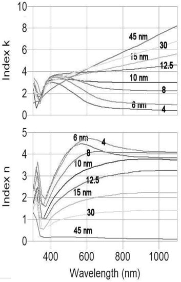
Evidence that the indices of metal vary with thickness in films less than some thickness is shown in Figure 1a,b (n and k) from the work of Hernandez-Mainet et al. [12]. Here the indices of their silver (Ag) films are plotted for their measured thicknesses (further effective thicknesses), by a quartz crystal monitor (QCM), of 6, 10, 15, and 45 nm. These measurements at a thickness of 45 nm are essentially like those of bulk silver. These indices are also similar to those of Willey et al. [13] as seen in Figure 2a,b comparing Hernandez, Willey, and Medwick et al. [14] Ag films, all films at 10 nm effective thickness. Figure 2a,b also demonstrate that results are influenced by the materials and processes used to deposit the films. Apparently, Medwick found a combination which makes the 10 nm Ag have similar indices to bulk silver. This seems to imply that the Ag coalesced/percolated before reaching 10 nm thick, as will be discussed below. This would allow Medwick’s group to design without considering the variation of indices with thickness, since the indices in the region around 10 nm and thicker would behave like the bulk indices. However, with processes such as those of Hernandez and Willey, it would be necessary to consider the index variation with thickness to obtain meaningful designs. Figure 3a,b and Figure 4a,b show the indices versus thickness such as Figure 1a,b for Hernandez but are for depositions of Medwick and Willey.
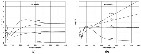
Figure 1.
(a) Real values of index for various thicknesses of silver layers reported by Hernandez-Mainet et al. [12]. (b) Imaginary values of index for various thicknesses of silver layers reported by Hernandez-Mainet et al. [12].
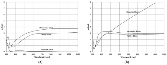
Figure 2.
(a) Real part of index of refraction comparing Hernandez, Willey, and Medwick Ag films, all at 10 nm thick. (b) Imaginary part of index of refraction comparing Hernandez, Willey, and Medwick Ag films, all at 10 nm thick.
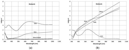
Figure 3.
(a) Real values of index for various thicknesses of silver layers reported by Medwick et al. [14]. (b) Imaginary values of index for various thicknesses of silver layers reported by Medwick et al. [14].
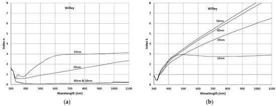
Figure 4.
(a) Real values of index for various thicknesses of silver layers reported by Willey et al. [13]. (b) Imaginary values of index for various thicknesses of silver layers reported by Willey et al. [13].
One possible approach to achieving homogeneous results such as those of Medwick is indicated by Formica et al. [15]. They used 1 nm Cu as the “wetting layer” for 6 nm of Ag and reduced the AFM surface roughness by an order of magnitude from the unwetted 6 nm Ag as evidenced in Figure 5 and Figure 6 (copied from their paper). It appears that 1 nm of Cu is the “magic bullet” to obtain very thin percolated Ag films. Figure 5 shows how the resistivity of the Cu/Ag film drops low at much thinner layers than for Ag only. Figure 6 shows that less than 1.0 nm of Cu is adequate to achieve this low roughness and bulk-like behavior. We would like to emphasize that it is our intention to reproduce (here and in some of the later pictures) the original graphs as an expression of our appreciation of these pioneering works, although some of the details of the scanning electron micrographs (SEM) may be not so well resolved. However, it should be obvious that in Figure 6, the SEM image on left (without seed layer) shows a much stronger pronounced surface structure that than with seed layer (on right), which practically looks structureless. Chen et al. [16] obtained similar results with a germanium (Ge) wetting layer, but less of an effect. Of course, when regarding transmittance or reflectance of the silver-coated surface, one has to take into account that the optical response is now defined by the combined effect of the silver film and the seed layer.
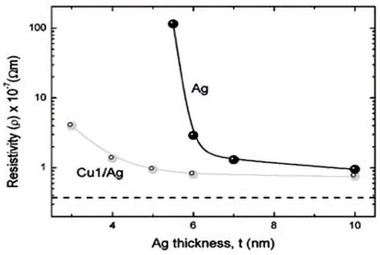
Figure 5.
Comparison of electrical resistivity variation for Ag films with and without a Cu seed layer. The dashed line represents the resistivity of bulk Ag film of about 300 nm thickness deposited using the same sputtering process. Both types of films shown here approaches bulk behavior with thickness >100 nm.
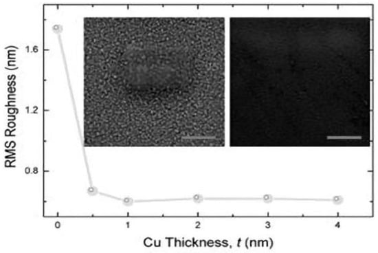
Figure 6.
Variation of RMS roughness for 6 nm Ag film with seed layer thickness. For seed layer thicknesses greater than 4 nm the RMS roughness has roughly the same values of about 0.6 nm. The inset shows the SEM pictures without (left) and with a Cu seed layer (right). The scale bars are 500 nm.
It appears that a key advantage of the designs reported by Medwick et al. [14] is that they have found a combination of materials and processes where the thin silver films (~10 nm) have n- and k-values much like the properties of bulk silver, where the n-values approach zero and the k-values are large.
Earlier related work on very thin silver films was conducted by Inagaki et al. [17] in 1986 with attenuated total reflection (ATR) geometry at 633 nm by the photoacoustic method. In 1989, Xu and Tang [18] reported on more extensive work using the ATR method with silver and other materials. They pointed out that the “films show great differences for the various materials and deposition methods.” Figure 7, copied from their paper, shows an interesting comparison between indices of thermally evaporated and magnetron sputtered silver at 640 nm. The thermal Ag seems to percolate by 15 or 16 nm, whereas the sputtered Ag has nearly the same effect by 4 nm.
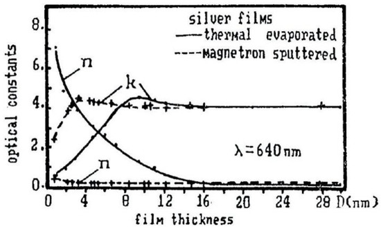
Figure 7.
Variations of the optical constants of silver island films with thickness: ___________, thermally evaporated silver films; - - - - - - -, magnetron sputtered films.
Willey et al. [13] showed more examples of the variation of percolation thickness with materials. Figure 8a,b show indices versus thickness of Ag deposited on fused silica (FS) in air, which seems to percolate at 30 nm. Figure 9a,b shows Ag deposited on FS which has been coated with 7 nm of Al2O3 (alumina) and the Ag capped with 7 nm of alumina. This seems to percolate at 20 nm.
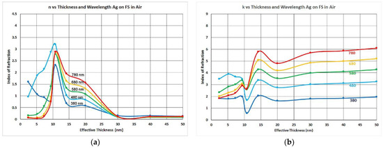
Figure 8.
(a) Real index of refraction versus thickness for various wavelengths as Ag is deposited on fused silica in air. (b) Imaginary index of refraction versus thickness for various wavelengths as Ag is deposited on fused silica in air.
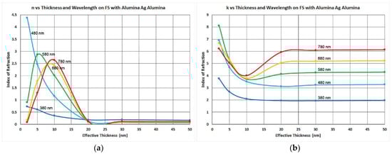
Figure 9.
(a) Real index of refraction versus thickness for various wavelengths a Ag is deposited on 7 nm of alumina and capped with 7 nm of alumina. (b) Imaginary index of refraction versus thickness for various wavelengths as Ag is deposited on 7 nm of alumina and capped with 7 nm of alumina.
These silver films are critical to the architectural and automotive window coating industries to control the emittance (E) for Low-E coatings and the %R and %T in general of their products. Thin chromium coatings are critical for making black mirrors. The behavior of a particular chromium deposition process can be seen in Figure 10 where n and k versus thickness are plotted on the same graph. Their behavior is somewhat different from silver, as can be seen from the Figure 10, in that there does not seem to be an obvious percolation effect, or perhaps it occurred at less than 15 nm.
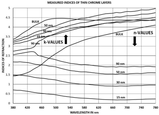
Figure 10.
Indices of measured witnesses of Cr on glass at various thicknesses as used in the double dispersion software (DDSW).
3. Results
3.1. Designing Black Mirrors with Variations in Indices
Designing a “black mirror” using chromium provides a good example of the application of the variable index with thickness capability. Figure 10 shows the indices of the chromium (Cr) versus thickness in nm of QCM readings derived from the %T and %R spectral measurements of real Cr depositions. It is understood that the QCM readings are not expected to represent the actual physical height of the Cr islands in layers prior to reaching a thickness where bulk properties are achieved. However, it is expected that the QCM would be used to control the thickness of these layers in production, and therefore it should repeat the results of the test depositions of Figure 10. Figure 11 shows the results of designing a black mirror coating to have no transmittance and a minimal reflection over the visual spectrum. The first layer is opaque Cr of 100 nm thickness. Then two layer-pairs of silica (SiO2) and thin Cr are deposited. Finally, a capping layer of silica is added. This provides a 6-layer coating which is the minimum number of layers for a practical black mirror. This first design uses only the bulk thickness indices from Palik [19] for all of the Cr layers. The silica is represented here by an index of 1.46 for simplicity. The design of the coating is: 100M 98.94L 13.61M 101.13L 4.62M 83.25L, which starts from the substrate, where M is the metal and L is the silica. However, if this coating design is deposited with these thicknesses but the indices were as in Figure 10, the resulting coating would have the spectrum seen in Figure 12 which would be useless as a black mirror. To rectify this problem, the design in Figure 11 is redesigned using the variable index for each metal layer thickness in what is referred to as the double dispersion software (DDSW), where the resulting spectrum would be as seen in Figure 13. The two dispersions are the usual horizontal dispersion with wavelength and the “vertical dispersion” is in index of refraction with layer thickness. The design of this coating is: 100M 91.71L 8.86M 101.71L 6.26M 68.82L. The design of Figure 11 has an average %R of 0.29% but is not realistic as stated, whereas that of Figure 13 is 0.33% and it is likely to be achievable.
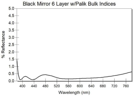
Figure 11.
Black mirror design of six layers using only the bulk thickness indices from Palik [19] for all of the Cr layers.
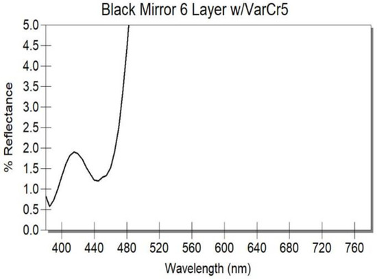
Figure 12.
Result of design of Figure 11 when actually deposited, because of variations of indices with thickness.
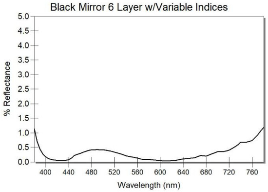
Figure 13.
Spectrum resulting from using double dispersion software (DDSW) to optimize design of Figure 11.
The above demonstrates the functioning and effectiveness of the DDSW approach. To further the demonstration, another layer-pair of silica and Cr were added to the design of Figure 13 to see what benefit could be gained and whether it would be worth the cost of two additional layers. Figure 14 shows the result of adding the two layers and optimizing, assuming the bulk values for Cr as in Figure 11. Figure 15 shows what would result if the design was deposited with these thicknesses, but that the process indices were as in Figure 10. Figure 16 is the spectrum which results when the design is conducted using the DDSW index process. The bottom line is that the above examples demonstrate the need for and benefits of considering the variation of indices with thickness which occurs in many materials when the layers are thinner than some realm of non-percolation of the island structure.
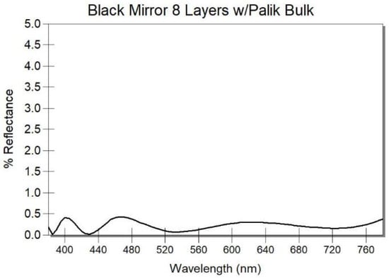
Figure 14.
Black mirror design of eight layers using only the bulk thickness indices from Palik [19] for all of the Cr layers.
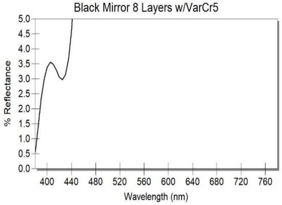
Figure 15.
Result of design of Figure 14 when actually deposited, because of variations of indices with thickness.
Figure 16.
Spectrum resulting from using double dispersion software (DDSW) to optimize design of Figure 14.
3.2. Designing Low-E Coatings with Variations in Indices
The work reported by Medwick et al. [14] will be used as an example of designing Low-E coatings. Figure 17 is reproduced from their Figure 8 showing the solar spectrum and the transmittance of two of Vitro’s Low-E products. The goal of the coating in the normal case is to transmit as much visible light as possible and reflect as much heat (infrared) as possible. Their spectral curve for Solarban 70XL glass will be used here as optimization targets except scaled up to have its maximum at 100%. Targets are also added for high infrared reflection and heat rejection from 850 to 1000 nm. It is assumed that the narrower spectral curve of the photopic response of the human eye is not as desirable in this application because the color rendering capability might be less than that of the broader curve of Figure 17.
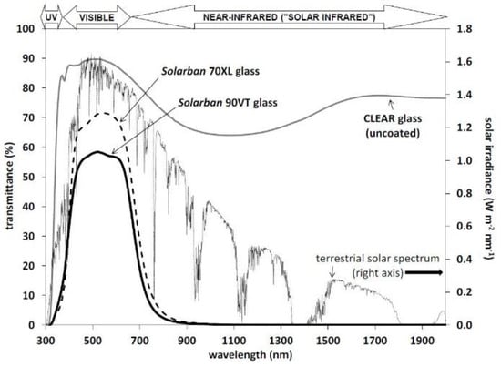
Figure 17.
Solar spectrum and the transmittance of two of Vitro’s Low-E products reproduced from Medwick et al. [14].
Medwick’s curve for the “CLEAR glass” has been helpful and it was also possible to estimate the indices of their dielectric material by reverse engineering from these spectral curves. These data are used here for designs meeting the Low-E requirements and approximating the 70XL design.
The indices for silver layers measured by Medwick’s group are shown in Figure 3a,b. Examples of interpolated values by the DDSW in integer nm thicknesses are plotted in Figure 18, Figure 19 and Figure 20.
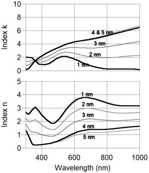
Figure 18.
Indices for 1 to 5 nm thick silver layers actually measured by Medwick (bold) and also interpolated with DDSW.
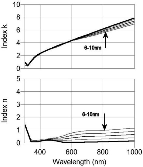
Figure 19.
Indices for 6 to 10 nm thick silver layers actually measured by Medwick (bold) and also interpolated with DDSW.
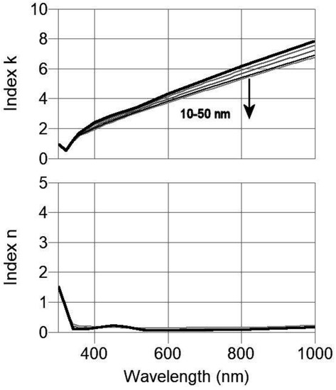
Figure 20.
Indices for 10 to 50 nm thick silver layers actually measured by Medwick (bold) and also interpolated with DDSW.
Medwick’s silver is somewhat different from what is seen in the work Willey et al. [13] and that reported by Hernandez-Mainet et al. [12]. This can be seen in Figure 1, Figure 2, Figure 3 and Figure 4. As discussed above, the Medwick materials and processes have the favorable effect that the near-bulk indices of refraction are maintained well below thicknesses of 10 nm as seen in Figure 19. As seen below, Figure 20 shows similar data for measured and interpolated thicknesses from the processes and materials of Hernandez. The changes in the indices with thickness are more gradual from bulk down to 6 nm of silver film thickness. The measured silver indices by Willey show similar results to that of Hernandez. As will be demonstrated below, it is difficult to impossible to obtain good Low-E performance without something such as the Medwick results.
Nadel [20] reviewed the history of the Low-E products of BOC Coating Technology (formerly Airco Coating Technology) up until 1996 as seen in Figure 21 where the early coatings used only one silver layer and later ones employed two silver layers. Medwick’s report shows three silver layers plus a special auxiliary layer.
Figure 21.
History of the Low-E products of BOC up until 1996 as reported by Nadel [20].
Figure 22 shows a simple single silver layer Low-E coating design with silica layers on both sides of the silver. This was optimized with respect to the targets shown by “+” signs derived from Medwick’s curve in Figure 17. The silica is simply represented by index 1.46 and the silver for the dashed line plot is using Medwick’s bulk values which results in a silver thickness of 13.81 nm. The solid line is after optimizing with the DDSW which results in a silver thickness of 11.23 nm. In Figure 22, Figure 23, Figure 24 and Figure 25, the dashed lines are all for designs using the indices for bulk silver (which are unrealistic), whereas the solid lines are all for using the realistic indices which are variable with thickness of the DDSW in the optimization process.
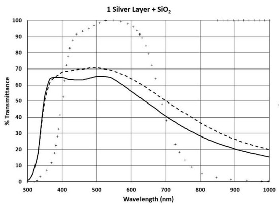
Figure 22.
Single silver layer Low-E coating design with silica layers on both sides of the silver. Dashed line is design with bulk silver indices, and solid line is with DDSW optimization.
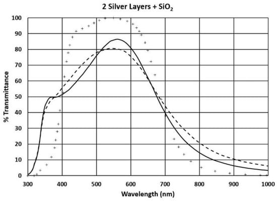
Figure 23.
Two silver layer Low-E coating design with silica layers on both sides of the silver. Dashed line is design with bulk silver indices, and solid line is with DDSW optimization.
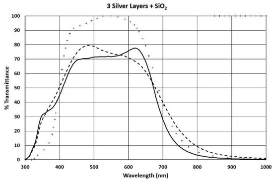
Figure 24.
Three silver layer Low-E coating design with silica layers on both sides of the silver. Dashed line is design with bulk silver indices, and solid line is with DDSW optimization.
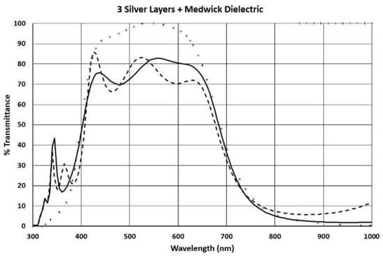
Figure 25.
Three silver layer Low-E coating design with Medwick’s dielectric layers on both sides of the silver. Dashed line is design with bulk silver indices, and solid line is with DDSW optimization.
The single silver layer design of Figure 22 somewhat suppresses the transmittance of the infrared and enhances the visible, but only to a limited extent. The design of Figure 23 with two silver layers suppresses the transmittance of the infrared quite a bit more. The three-silver layer version in Figure 24 approximates Medwick’s results much better.
The designs of these three figures using the bulk silver indices, as well as the designs of these three figures using the variable thickness silver DDSW indices, are given in Table 1:

When the estimated dielectric material from Medwick’s work is substituted for the silica in the three-layer design of Figure 24 and reoptimized, Figure 25 results. This is generally like the Figure 24 design with the exception of spikes between 300 and 400 nm. It is suspected that the real dielectric materials used by Medwick may not actually have this problem, but that our estimates of the indices of the dielectric materials are incomplete and/or inaccurate.
Figure 26, derived from the report of Hernandez-Mainet et al. [12], are indices to be compared with Figure 18, Figure 19 and Figure 20 derived from Medwick et al. [14]. The silver materials and process of Hernadez do not become fully bulk-like until they are thicker than 30 nm, whereas those of Medwick are nearly bulk-like soon after 6 nm. It appears that the combination of low n-values and high k-values is important for good Low-E coatings. The difficulty of achieving a good Low-E design with the silver processes reported by Hernandez or Willey will be demonstrated by attempting to repeat the work of Medwick reported in Figure 22, Figure 23 and Figure 24 using the Hernandez silver indices.
The dashed line in Figure 27a shows a single layer of silver using Hernandez’s bulk indices surrounded by two layers of silica which have been optimized with respect to the targets shown in dots (which include the 100% reflectance targets from 850 to 1000 nm seen in the upper right of the figure). When those layers are optimized accounting for the variation of indices with thickness by the DDSW, the solid curve of Figure 27 is the result. Figure 27b,c show the same procedures applied to designs of two and three thin silver layers in silica. In these two cases, the optimization processes reduced all but one silver layer to zero thickness so that the results were the same as in Figure 27a. All of this demonstrates that the thin silver layers benefit by having as close to bulk silver indices as practical in whatever thickness they are used. It is conjectured that early investigators in the field of Low-E coatings may have designed with bulk indices and achieved good design results, and then found that deposited results were disappointing, as demonstrated in Figure 27a–c. The search to find material combinations and process parameters to produce the good design results could have been challenging.
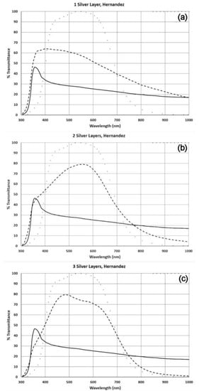
Figure 27.
Low-E coatings designed with Hernandez’s bulk indices values (dashed lines) but showing disappointing results when designed with more realistic thin layer indices (solid lines). Targets are shown as small “+” marks. Silver layers are surrounded by silica layers of optimized thicknesses. (a) shows designs with a single silver layer, (b) is a design with two silver layers, and (c) is a design with three silver layers.
Silver seems to be the nearest to an ideal metal (IM) in the visible spectrum. The properties of such an IM will be discussed below, but they will be applied first in the next two figures. In these figures, it is assumed that the bulk properties are maintained for all thicknesses of the IM that are needed in the designs. Indices for silica (SiO2, 1.46), alumina (Al2O3, 1.65), Medwick’s Dielectric (Zn2SnO4), and titania (TiO2) are tried in the designs. Figure 28a uses the first three dielectric materials and Figure 28b uses titania for the best result of all these. The lower curve in Figure 28a is with “real” materials and the upper three curves employ the IM. The unwanted spike at about 350 nm with the Zn2SnO4 may not exist, since we have only estimated the properties from the paper of Medwick et al. [14]. Figure 28b shows the desirable results of using titania to subdue the transmittance at shorter than 400 nm by titania’s natural absorbance in the ultraviolet spectrum. The actual use of titania in Low-E coatings would depend on whether its physical and chemical properties were consistent with the percolation and environmental durability needs of the real production processes.
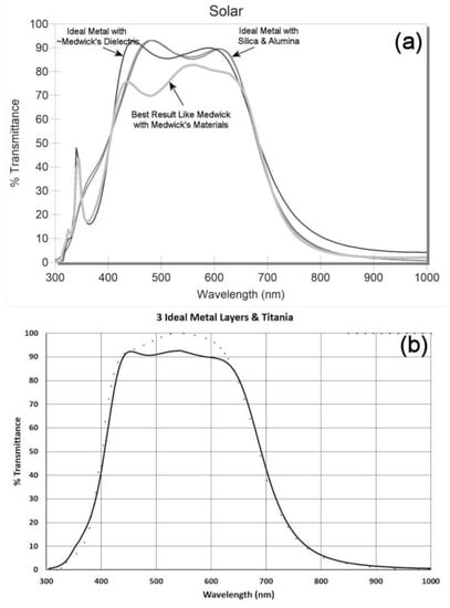
Figure 28.
(a) Best design using estimated materials from Medwick in lower curve. Three upper curves using ideal metal instead of silver with silica, alumina, and Medwick’s dielectric. (b) Design with three ideal metal layers and titania dielectric layers.
3.3. Properties of an Ideal Metal
The term “Ideal Metal” here refers to a metal whose n-values are all zero for all wavelengths larger than a certain threshold wavelength, and whose k-values are monotonically increasing with wavelength as shown in Figure 29a. Silver closely satisfies these requirements from near 500 nm to longer wavelengths as also shown in Figure 29a.
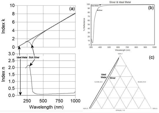
Figure 29.
(a) Comparison of the indices of refraction of an Ideal Metal with silver. (b) Comparison of the spectral reflectance of an ideal metal with silver. (c) Comparison on Apfel [21] triangle plots of an ideal metal with silver.
Generally, the specifics of the optical constants of bulk metals are caused by the presence of free electrons. The free electron fraction gives rise to a dielectric function ε defined by the Drude function (1):
where ω is the angular frequency, ωp the plasma angular frequency usually located deep in the ultraviolet, and γ the Drude damping parameter. Typically, . From the dielectric function, the optical constants n and k of non-magnetic materials are calculated by (2):
Equations (1) and (2) together result in the typically observed behavior that the refractive index of bulk metals is smaller than 1 in broad spectral regions, while k >> n. The ideal metal IM is obtained from (1) when setting γ = 0. Indeed, in this case, from (1) we have:
which is negative whenever is fulfilled. Then, from (2), the refractive index of an IM turns out to be zero, while k is different from zero according to . This gives rise to the observed increase of k with increasing wavelength for nearly ideal bulk metals.
In practice, bulk silver has a refractive index in the range between 0.1 and 0.2 in the visible spectral range [19]. The refractive index of silver is thus much smaller than one, so that silver is rather close to an ideal metal with respect to its optical properties. Note that a silver island film with well-segregated islands is no more comparable to bulk silver, because it has a much larger electric resistivity (see Figure 5). The reason is in the lack of electric conduction paths in an island film, and therefore, the island film rather behaves like a dielectric, which typically has a refractive index larger than one. As a result, it is not astonishing that the refractive index in Figure 1 or Figure 3 tends to increase with decreasing film thickness. The concrete n-values strongly depend on the geometry of the islands and the properties of the ambient of the islands, as it will be discussed later in Section 4.1. In particular, chemical reactions at the metal island surface such as oxidation may have a tremendous effect on the optical properties of an island film.
Figure 29b compares the normal incidence reflectance of bulk silver with that of the IM, which is 100%. The IM has no transmittance or absorbance as shown in the Apfel [21] triangle diagram of Figure 29c. Here the silver plot stays close to the 0% absorptance line between 100%T and 100%T having little absorptance; the line for the IM is exactly on that line with 0% absorptance.
Figure 30a shows the reflectance amplitude plot for silver evaluated at 550 nm. The IM would look very similar except that the opaque point for IM would be exactly on the outer circle near the 10 o’clock position (depending on the wavelength), whereas the silver opaque point is somewhat inside the circle.
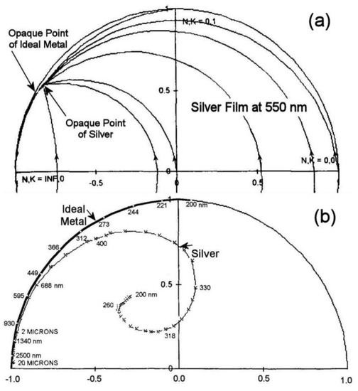
Figure 30.
(a) Reflectance amplitude plot for silver evaluated at 550 nm. (b) Opaque points versus wavelength on a reflectance amplitude plot for silver and for an ideal metal.
Figure 30b shows the opaque points versus wavelength on a Reflectance Amplitude plot for silver and for the IM. Opaque points for the IM are all on the 100% reflectance outer circle, and their positions move counterclockwise with increasing wavelength as seen in Figure 30b. This shows that the silver has a lot of absorptance below 400 nm whereas the IM has none.
4. Discussion
4.1. Relation to Mixing Models
Formally, the metal island films discussed here represent a special case of physical mixtures. In the literature, there are different approaches to calculate the optical constants of a mixture, provided that the optical constants of its constituents are known [22,23,24,25,26,27]. Let us shortly discuss some often used approaches in order to highlight the relation of our approach to these models. Note that the description is usually performed in termini of the dielectric function ε, and not in termini of optical constants n and k. In non-magnetic materials, they are related to each other via (2).
For a quantitative description of the optical properties of mixtures, we assume that each of the constituents is characterized by the dielectric function and occupies a certain volume fraction . This volume fraction defines the filling factor of the material j via:
where V is the full volume occupied by the mixture. Obviously,
there is a first group of traditional mixing models that is essentially based on the local field theory [28,29]. They can all be derived from the assumption that the mixing partners are tackled as inclusions numbered by the subscript j, embedded in a certain host medium with a dielectric function εh [30]. Note that here all inclusions should be small enough such that the mixture still appears optically homogeneous. This assumption leads to the general mixing formula [31]:
Here L is the so-called depolarization factor which allows taking the specific geometry of the conclusions into account. is the effective dielectric function of the mixture. Note that holds. In the case of spherical inclusions, L = 1/3, and in this case a more familiar writing of (6) is obtained:
Generally, it is thus an advantage of this group of mixing models, that they allow considering the specific geometry of the material inclusions explicitly. If reliable information on the mixing geometry is available, (6) should be regarded the best choice for modelling the optical constants of the mixture. In particular, when taking into account that the IM has a negative dielectric function, (6) or (7) describe resonant behavior when one of the denominators in (7) becomes small (localized surface plasmon excitation). It is thus the relation between the optical properties of the metal and the embedding dielectric that is crucial for the optical properties of the mixture, i.e., here the metal island film.
In fact (6) or (7) describe not only a single mixing model, but rather a group of models, which differ in the choice of εh. For εh =1, from (7) we obtain the Lorentz–Lorenz mixing formula, and for the Bruggeman formula, also known as effective medium approximation (EMA). Alternatively, εh can be set equal to the dielectric function of any of the mixing partners, which results in the Maxwell–Garnett model.
It is that ambiguity with respect to the choice of εh that makes the application of (6) difficult in practice, when no detailed information about the morphology of the mixtures is available. In fact, εh cancels out only in the limiting cases L = 0 and L = 1:
In binary dielectric mixtures, (8) and (9) define the so-called Wiener bounds of the dielectric function of a binary mixture [29].
There is another group of mixing models which is free from that ambiguity, but is of rather empirical structure, namely the Lichtenecker formula [32]. It can be written as:
Note that the limiting cases of β = 1 and β = −1 coincide with the expressions (8) and (9), correspondingly. The case β = 1/2 obviously corresponds to a linear superposition of complex refractive indices, as it follows from (2). It has proven useful in the practice of rugate filter design, where modelling the optical properties of dielectric mixtures is essential [33]. For β = 1/3, from (10) we obtain the Looyenga mixing formula [28]. Information on the morphology of the mixture does not enter explicitly into (10).
Therefore, the local-field-based equation (6) seems theoretically superior to the rather empirical Lichtenecker approach. With regard to the applicability to optical film property modelling in optical coating practice; however, the picture may change. The point is that in a real metal island film as produced by evaporation in vacuum, there is a stochastic distribution of the metal islands with respect to size, inter-island distances, island shapes, and orientations. This is exemplified in Figure 31.
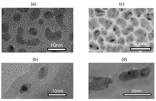
Figure 31.
Transmission electron micrographs of selected copper island films. (a) 1.7 nm thick copper island film: top view (b) 1.7 nm thick copper island film: cross section; (c) 6.8 nm thick copper island film: top view; (d) 6.8 nm thick copper island film: cross section.
Figure 31 shows transmission electron micrographs of two copper island films embedded in alumina. The preparation technique is described in [7]. The first film (images (a) and (b)) corresponds to an effective copper thickness of approximately 1.7 nm, the second film (images c) and (d)) to approximately 6.8 nm. Both films are shown in top view ((a) and (c)) as well as from the side, i.e., as cross-section images ((b) and (d)). The copper islands, which are seen as dark spots, show obvious differences in size and shape, the latter being far from a spherical one. The electron micrographs have been obtained at Ulm University, Dept. Materialwissenschaftliche Elektronenmikroskopie.
For reliable modelling of such systems one would have at least to investigate the statistical distribution g(L) of the L-factors in (6), and then to average the modelled dielectric function over all possible depolarization factors. For the particular case of the Maxwell–Garnett model, this is exemplified in [9]. It is demonstrated there, that physically reasonable peak positions and linewidth of the usually observed localized plasmon resonance in the metal islands may be predicted this way. In coating design and deposition practice, this information on the island statistics is usually not available. This also prevents the application of the elegant Bergman theory [29] in coating manufacturing practice.
Therefore, our approach basically makes use of the Lichtenecker formula, in our case setting β = ½, although this choice is not of principal nature. Then, the filling factor p may be related to what we call the island film effective thickness. The crucial point is in the choice of the mixing partners: instead of trying to describe the mixing between a metal and a dielectric material by such kind of linear superposition of their complex refractive indices (which would surely result in unreasonable optical constants), we mix the known optical constants of two island films with a different effective thickness (and different p). This way the important information on the film morphology (including any extrinsic or intrinsic size effects [29]) does not enter into the calculation explicitly through a statistical distribution of depolarization factors, but implicitly through the specific behavior of the optical constants of the chosen constituents of the mixture. Provided that reliable optical constants are available at a sufficiently narrow grid of thickness values (for characterization methods see for example [22,34,35]), the calculated by (10) optical constants for in-between falling thicknesses are expected to be realistic as it will be discussed in the next section.
4.2. Limits of the DDSW Approach
Although the frequency dependence of optical constants (the usual dispersion) is theoretically well understood and formulated in terms of analytical dispersion laws [11,28,31], at present it is impossible to indicate comparably convenient analytic formulas for describing the thickness dependence of optical constants (which we call “vertical dispersion” here). In fact, as it is seen from Figure 1, Figure 2, Figure 3 and Figure 4, that dependence will be rather complex and in general nonlinear. Therefore, even when we make use of a sufficiently narrow grid of experimental dispersion curves determined at different film thicknesses, the linear interpolation for in-between falling thicknesses remains an approximation. On the other hand, the approach is robust and applicable in a coating production environment, which we regard a tremendous advantage of this method. This section is to discuss some relative advantages and disadvantages of the mentioned interpolation approach.
With respect to interpolation in the DDSW, if it is suspected that the change in indices is not sufficiently linear between already measured thicknesses, one or more additional thicknesses can be measured and interposed to accommodate the nonlinearity. An extreme case is illustrated in Figure 32a, where the resonance peaks in k-value for two witness sample thicknesses are separated by 300 nm in wavelength. The dashed line shows what the interpolation results with the current DDSW would look like in the dashed line. This is clearly not a good representation of reality. Figure 32b shows the case for even as little as 20 nm separation in the resonance peaks, where there is still some error in the vertical direction. To correct this limitation requires two-dimensional interpolation in both index (vertical) and wavelength (horizontal) which is delt with below. However, the practical applications which have been examined here do not seem to suffer from this limitation. Figure 33, from Medwick et al. [14], shows the wavelength shift with layer thickness in a real-world example of very thin silver layers. The severity of this limitation seems to be related to the aspect ratio of the vertical scale to the wavelength scale. Stenzel [22] has extensive discussions of these subjects and many example curves of n- and k-values versus wavelength, particularly in Chap. 12 on metal island films. It seems that all Stenzel’s figures would be reasonably well represented by the current DDSW interpolations.
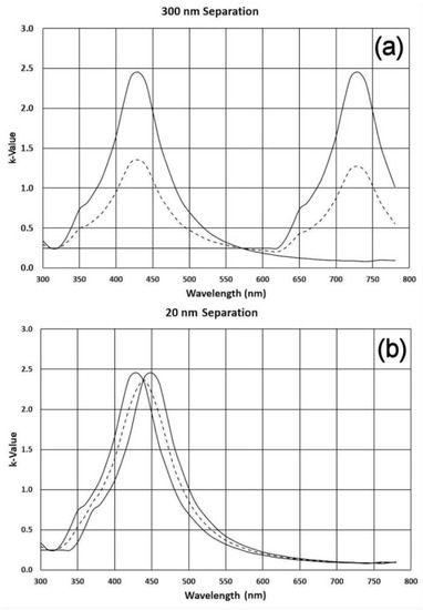
Figure 32.
(a) Resonance peaks in k-values 300 nm apart for two thicknesses of metal island films. Dashed line shows erroneous interpolation. (b) Resonance peaks in k-values only 20 nm apart for two thicknesses of metal island films. Dashed line shows erroneous interpolation.
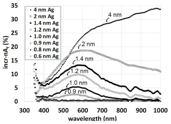
Figure 33.
Medwick’s Figure 2 showing various thicknesses of silver films wherein the simple interpolation should not be a problem. Note that the response of the thinnest two layers is practically coinciding with the abscissa.
4.3. The Triple Dispersion Software (TDSW) Approach
The earlier publication [13] on the DDSW approach was limited to interpolation in the vertical direction only. The interpolation in the additional dimension to solve the problem of Figure 32 has recently been worked out. This new approach is designated as triple dispersion software (TDSW) to differentiate it from DDSW. Figure 34 shows a simulation of two measured thicknesses of indices plotted in solid curves plus three interpolated thicknesses plotted in dashed curves. The first steps in the interpolation process are to determine the peaks of the two measured curves and interpolate the peak position for the thickness to be interpolated. Figure 35 shows the next steps which are to shift the measured curves in wavelength to match at the new peak wavelength and to scale each of the measured curves to match the new peak magnitude. Figure 36 shows these new curves of Figure 35 on an expanded scale. In this case, interpolated wavelength values of 75% between the first and second measured and scaled curves all at the same selected magnitude (vertical) levels are calculated. The resulting interpolated curve is the desired result as seen in Figure 37 in the dashed curve between the two solid curves for the measured values.
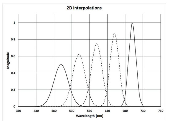
Figure 34.
Simulation of two measured thicknesses of indices plotted in solid curves plus three interpolated thicknesses plotted in dashed curves.
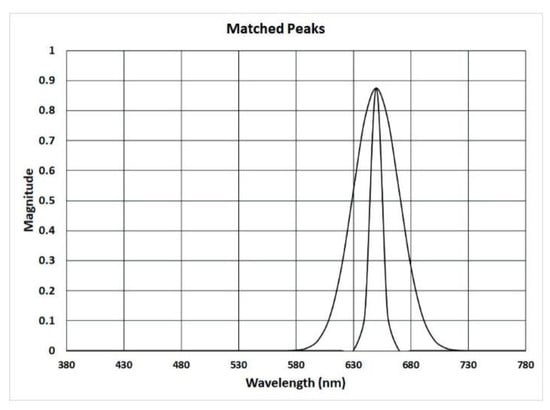
Figure 35.
Shift the measured curves in wavelength to match at the new peak wavelength and to scale each of the measured curves to match the new peak magnitude.
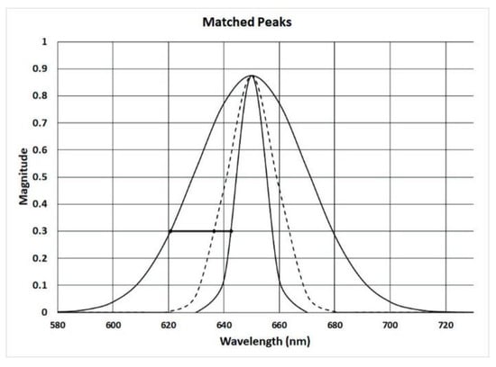
Figure 36.
Curves of Figure 35 on an expanded scale. In this case, interpolated wavelength values of 75% between the first and second measured and scaled curves all at the same selected magnitude (vertical) levels as calculated.
Figure 37.
Resulting interpolated curve is the desired result in the dashed curve between the two solid curves for the measured values.
Figure 38 shows similar hypothetical curves of k-value of index of refraction cases where the peak shifts in wavelength and magnitude. The TDSW process is applied here for changes in thickness of 25%, 50%, and 75% from the highest peak to the lowest peak of the measured values. This figure points out two residual limitations of even the TDSW approach which are circled in the figure. The circle on the left shows that the wavelength range of the interpolated vales become truncated to only those wavelengths which are common to both measured curves after shifting to the interpolated wavelength. The circle on the right shows that any features in the two measured curves which do not shift in wavelength with thickness may be distorted.
Figure 38.
Hypothetical curves of k-value of index of refraction cases where the peak shifts in wavelength and magnitude.
The thrust of the present work has been to make a practical tool for the thin film designer to be able to design optical thin films on the order of 10 nm thick or less with a reasonable expectation of obtaining the same results when those designs were fabricated. No explicit formulation of a mixing model of type (6) or (7) needs to be assumed here.
4.4. Closed Ultrathin Metal Films
Clearly, thickness-dependent optical constants in ultrathin metal films may be observed even when the films are closed. In Figure 39, three scenarios are visualized which may—for different reasons—give rise to thickness-dependent optical constants.
Figure 39.
(a) metal island film; (b) closed smooth ultrathin metal film; (c) rough metal film as a superposition of situations (a,b).
Figure 39a shows a schematic picture of a metal island film. In general, its effective optical constants may change when changing shape, size, and distance between the islands. Typically, all the mentioned geometrical parameters are dependent on the effective film thickness (compare [7]), which results in the observed thickness dependence of the effective optical constants of metal island films.
Nevertheless thickness-dependent optical constants in ultrathin metal films may be observed even when the films are closed and smooth (Figure 39b). An example is provided by mean free path effects which occur when the film thickness (here dc) is smaller than the mean free path a conduction electron in the corresponding bulk material would have [36,37,38]. Representative data for the mean free path of conduction electrons in bulk metals may be found for example in [39], for typical metals it ranges between several nanometers and a few nanometer decades; it is thus in agreement with the thickness range that is in the focus of our study.
Therefore, the methodology developed in the present study may also be applied to design problems that include such types of closed but ultrathin metal films. It has thus a rather broad application potential that may be extended to design procedures of modern optical elements such as magneto-optical hypercrystals [40] or photonic crystals with topological bandgaps [41].
For rough metal films in the thickness range of one or a few nanometer decades, the Figure 39c may be of practical relevance. It shows a rough closed metal film as a superposition of a closed smooth film with metal island films on its surfaces. Clearly, the closed part of the rough film and its surface areas provide different contributions to the full optical response of the rough film. Then, if the total thickness d is much smaller than the incident wavelength, the effective optical constants of the rough film may be modelled as a biased superposition of the optical response of the closed part of the film and the two island films on the surface. The situation is similar to what has been developed earlier for modelling optical constants in dielectric rugate filters (“flip-flop” method [42]), where a sequence of ultrathin high- and low-index layers is used to model a medium refractive index. The particular relations between dc and disland film (Figure 39c) may again result in a thickness dependence of the resulting effective optical constants of the rough film, which will be specific for the chosen materials and film preparation methods.
We finally note that as an alternative approach, metal island films as well as rough closed metal films have successfully been modelled in terms of the rigorous coupled wave approach (RCWA) [43,44]. In these models, the geometric features of the island assemblies or the surface roughness profile are assumed to obey strong lateral periodicity.
5. Summary
It was the primary purpose of this study to develop and describe an approach that allows considering the thickness dependence of optical constants in a practical optical coating design procedure. The focus was on conceptual simplicity and robustness in order to make the method applicable for use in a coating manufacturing environment. In manufacturing conditions, spectrophotometric or spectral ellipsometric thin film characterization is usually available, while there is usually a lack of sophisticated characterization tools for investigating the submicrometer or nanostructure of films (electron microscopy, X-ray diffraction or the like). Therefore, our method makes use of optical constants determined from differently thick films and the corresponding thicknesses as the only input parameters.
The need for and advantages of double dispersion software (DDSW) as well as triple dispersion software (TDSW) to accomplish interpolation of optical constants has been demonstrated. The need for silver and associated materials and processes to provide thin silver layers which have bulk-like indices has been shown in terms of practical examples. Design calculations were presented for two circles of problems: Low-E coatings for architectural glasses and black mirrors. Both examples verify the effectiveness of the developed interpolation procedures.
The developed approach has been discussed in relation to two classes of optical mixing models: The first class is based on the local field theory and embodies such important models such as the Lorentz–Lorenz model, the Maxwell–Garnett approach, and the Bruggeman effective medium theory. The second class is based on the Lichtenecker formula, and our approach may be treated as an adapted version of that Lichtenecker approach. Its robustness is primarily caused by the special choice of the input optical constants: Instead of making use of bulk optical constants of pure materials, in our approach experimental optical constants that stem from relevant reference samples are directly used. As a consequence, the method is not limited to island films, but also to closed films with thickness-dependent optical constants.
The effects of seed layers on the properties of the subsequently deposited metal films have been briefly addressed. Seed layers are of practical use for reducing the surface roughness of rather thick metal reflector coatings, and thus maximize their reflectance [45,46]. If the metal reflector film is sufficiently thick, no incident light will reach the seed layer, so that the optical constants of the seed layer are of no relevance for the measured reflectance.
Let us finally mention the tremendous significance of any kind of ultrathin metal films in the design of so-called plasmonic solar cells (for reviews see [47,48]), as well as for metamaterials [49] and metasurfaces [50]. These modern research and development directions define further application fields of design tools specified to deal with metal films with thickness-dependent optical constants.
Author Contributions
Conceptualization, R.R.W.; methodology, R.R.W.; software, R.R.W..; validation, R.R.W. and O.S.; formal analysis, R.R.W. and O.S.; investigation, R.R.W. and O.S.; resources, R.R.W. and O.S.; data curation, R.R.W. and O.S.; writing—original draft preparation, R.R.W..; writing—review and editing O.S.; visualization, R.R.W. and O.S.; funding acquisition, O.S. All authors have read and agreed to the published version of the manuscript.
Funding
Part of this research was funded by BMWi, Germany grant number TAILOR grant16IN0665.
Institutional Review Board Statement
Not applicable.
Informed Consent Statement
Not applicable.
Data Availability Statement
All data that support the findings of this study are included within the article.
Acknowledgments
R. Willey acknowledges the extensive support for this work in augmenting FilmStar Software provided by Fred T. Goldstein of FTG Software in Princeton, N. J. (www.ftgsoftware.com, accessed on 2nd February 2023). O. Stenzel is grateful to M. Held, Beschichtungstechnik Elsoff, for preparing copper island films, and to M. Biskupek and U. Kaiser, University Ulm, for transmission electron analysis. Thanks are also due to S. Wilbrandt for his interest to this study, assistance and helpful hints. Parts of this study have been supported by the BMWi, Germany, in terms of the TAILOR grant16IN0665.
Conflicts of Interest
The authors declare no conflict of interest.
References
- Kaiser, N. Review of the fundamentals of thin-film growth. Appl. Opt. 2002, 41, 3053–3060. [Google Scholar] [CrossRef]
- Janicki, V.; Amotchkina, T.V.; Sancho-Parramon, J.; Zorc, H.; Trubetskov, M.K.; Tikhonravov, A.V. Design and production of bicolour reflecting coatings with Au metal island films. Opt. Express 2011, 19, 25521–25527. [Google Scholar] [CrossRef]
- Janicki, V.; Sancho-Parramon, J.; Zorc, H. Gradient silver nanoparticle layers in absorbing coatings—Experimental study. Appl. Opt. 2010, 50, C228–C231. [Google Scholar] [CrossRef] [PubMed]
- Kachan, S.; Stenzel, O.; Ponyavina, A. High-absorbing gradient multilayer coatings with silver nanoparticles. Appl. Phys. B Laser Opt. 2006, 84, 281–287. [Google Scholar] [CrossRef]
- Gläser, H.J. Dünnfilmtechnologie auf Flachglas; Hofmann-Verlag GmbH & Co. KG: Schorndorf, Germany, 1999; pp. 164–248. [Google Scholar]
- Abelès, F. Optical Properties of Thin Absorbing Films. J. Opt. Soc. Am. 1957, 47, 473–482. [Google Scholar] [CrossRef]
- Held, M.; Stenzel, O.; Wilbrandt, S.; Kaiser, N.; Tünnermann, A. Manufacture and characterization of optical coatings with incorporated copper island films. Appl. Opt. 2012, 51, 4436–4447. [Google Scholar] [CrossRef]
- Stenzel, O.; Heger, P.; Bischoff, M.; Wilbrandt, S.; Kaiser, N. “Novel Optical Coating Concepts Based on Nanostructured Thin Solid Films”: Physics, Chemistry and Application of Nanostructures, Borisenko, V., Gaponenko, S., Gurin, V., Eds.; World Scientific Publishing: Singapore, 2005; pp. 28–35. [Google Scholar]
- Stenzel, O.; Macleod, A. Metal-dielectric composite optical coatings. Adv. Opt. Technol. 2012, 1, 463–481. [Google Scholar]
- Available online: https://www.codixx.de/en/knowledge-corner/polarization (accessed on 11 January 2023).
- Born, M.; Wolf, E. Principles of Optics; Pergamon Press: Oxford, UK; Edinburgh, NY, USA; Paris, France; Frankfurt, Germany, 1968. [Google Scholar]
- Hernandez-Mainet, L.C.; Aguilar, M.A.; Tamargo, M.C.; Falcony, C. Design and engineering of IZO/Ag/glass solar filters for low-emissivity window performance. Opt. Eng. 2017, 56, 1. [Google Scholar] [CrossRef]
- Willey, R.R.; Valavicius, A.; Goldstein, F.T. Designing with very thin optical films. Appl. Opt. 2020, 59, A213–A218. [Google Scholar] [CrossRef]
- Medwick, P.A.; Wagner, A.V.; Fisher, P.J.; Polcyn, A.D. Nanoplasmonic (“Sub-Critical”) Silver as Optically Absorptive Layers in Solar-Control Glasses. In Proceedings of the 60th Annual Society of Vacuum Coaters Technical Conference, Providence, RI, USA, 29 April–4 May 2017. [Google Scholar]
- Formica, N.; Ghosh, D.S.; Carrilero, A.; Chen, T.L.; Simpson, R.E.; Pruneri, V. Ultrastable and Atomically Smooth Ultrathin Silver Films Grown on a Copper Seed Layer. ACS Appl. Mater. Interfaces 2013, 5, 3048–3053. [Google Scholar] [CrossRef]
- Chen, W.; Thoreson, M.D.; Ishii, S.; Kildishev, A.V.; Shalaev, V.M. Ultra-thin ultra-smooth and low-loss silver films on a germanium wetting layer. Opt. Express 2010, 18, 5124–5134. [Google Scholar] [CrossRef] [PubMed]
- Inagaki, T.; Goudonnet, J.P.; Royer, P.; Arakawa, E.T. Optical properties of silver island films in the attenuated-total-reflection geometry. Appl. Opt. 1986, 25, 3635–3639. [Google Scholar] [CrossRef]
- Xu, J.-J.; Tang, J.-F. Optical properties of extremely thin films: Studies using ATR techniques. Appl. Opt. 1989, 28, 2925–2928. [Google Scholar] [CrossRef]
- Palik, E.D.; Palik, X.E. Handbook of Optical Constants of Solids II; Academic Press: Boston, FL, USA, 1991; pp. 374–387. [Google Scholar]
- Nadel, S. Advanced Low-Emissivity Glazings. In Proceedings of the 39th Annual Technology Conference Proceedings, Philadelphia, PA, USA, 5–10 May 1996. [Google Scholar]
- Apfel, J.H. Triangular coordinate graphical presentation of the optical performance of a semi-transparent metal film. Appl. Opt. 1990, 29, 4272–4275. [Google Scholar] [CrossRef] [PubMed]
- Stenzel, O. Optical Coatings, Material Aspects in Theory and Practice; Springer: Berlin/Heidelberg, Germany, 2014. [Google Scholar]
- Theiss, W. The Use of Effective Medium Theories in Optical Spectroscopy. In Festkörperprobleme/Advances in Solid State Physics 33; Vieweg Braunschweig: Kranzberg, Germany, 1993; pp. 149–176. [Google Scholar]
- Goncharenko, A.V.; Lozovski, V.Z.; Venger, E.F. Lichtenecker’s equation: Applicability and limitations. Optics Comm. 2000, 174, 19–32. [Google Scholar] [CrossRef]
- Menegotto, T.; Pereira, M.B.; Correia, R.R.B.; Horowitz, F. Simple modeling of plasmon resonances in Ag=SiO2 nanocomposite monolayers. Appl. Opt. 2011, 50, C27–C30. [Google Scholar] [CrossRef]
- Protopapa, M.L. Simulation of optical properties of layered metallic nanoparticles embedded inside dielectric matrices: Interference method or Maxwell Garnett effective-medium theory? Appl. Opt. 2010, 49, 3014–3024. [Google Scholar] [CrossRef]
- Niklasson, G.A.; Granqvist, C.G.; Hunderi, O. Effective medium models for the optical properties of inhomogeneous materials. Appl. Opt. 1981, 20, 26–30. [Google Scholar] [CrossRef]
- Landau, L.; Lifshitz, E. Electrodynamics of Continuous Media ( Volume 8 of A Course of Theoretical Physics); Pergamon Press: Oxford, UK, 1960; pp. 36–47. [Google Scholar]
- Kreibig, U.; Vollmer, M. Optical Properties of Metal Clusters; Springer Series in Materials Science; Springer: Heidelberg, Germany, 1995; Volume 25, pp. 123–184. [Google Scholar]
- Aspnes, D.; Theeten, J.; Hottier, F. Investigation of effective-medium models of microscopic surface roughness by spectroscopic ellipsometry. Phys. Rev. B 1979, 20, 3292–3302. [Google Scholar] [CrossRef]
- Stenzel, O. The Physics of Thin Film Optical Spectra: An Introduction“ Springer Series in Surface Sciences 44, 2nd ed.; Springer: Berlin/Heidelberg, Germany, 2015; pp. 57–71. [Google Scholar]
- Leão, T.P.; Perfect, E.; Tyner, J.S. Evaluation of Lichtenecker’s mixing model for predicting effective permittivity of soils at 50 MHz. Trans. ASABE 2015, 58, 83–91. [Google Scholar]
- Tikhonravov, A.; Trubetskov, M.; Amotchkina, T.; Kokarev, M.; Kaiser, N.; Stenzel, O.; SWilbrandt Gäbler, D. New optimization algorithm for the synthesis of rugate optical coatings. Appl. Opt. 2006, 45, 1515–1524. [Google Scholar] [CrossRef]
- Amotchkina, T.V.; Janicki, V.; Sancho-Parramon, J.; Tikhonravov, A.V.; Trubetskov, M.K.; Zorc, H. General approach to reliable characterization of thin metal films. Appl. Opt. 2011, 50, 1453–1464. [Google Scholar] [CrossRef]
- Amotchkina, T.V.; Trubetskov, M.K.; Tikhonravov, A.V.; Janicki, V.; Sancho-Parramon, J.; Zorc, H. Comparison of two techniques for reliable characterization of thin metal-dielectric films. Appl. Opt. 2011, 50, 6189–6197. [Google Scholar] [CrossRef]
- Anderson, J. Conduction in thin semiconductor films. Adv. Phys. 1970, 19, 311–338. [Google Scholar] [CrossRef]
- Weißmantel, C.; Hamann, C. Grundlagen der Festkörperphysik; Springer: Berlin, Germany, 1979; pp. 413–416. [Google Scholar]
- Stenzel, O.; Wilbrandt, S.; Stempfhuber, S.; Gäbler, D.; Wolleb, S.-J. Spectrophotometric Characterization of Thin Copper and Gold Films Prepared by Electron Beam Evaporation: Thickness Dependence of the Drude Damping Parameter. Coatings 2019, 9, 181. [Google Scholar] [CrossRef]
- Gall, D. Electron mean free path in elemental metals. J. Appl. Phys. 2016, 119, 085101. [Google Scholar] [CrossRef]
- Hu, S.; Song, J.; Guo, Z.; Jiang, H.; Deng, F.; Dong, L.; Chen, H. Omnidirectional nonreciprocal absorber realized by the magneto-optical hypercrystal. Opt. Express 2022, 30, 12104–12119. [Google Scholar] [CrossRef] [PubMed]
- Huang, Q.; Guo, Z.; Feng, J.; Yu, C.; Jiang, H.; Zhang, Z.; Wang, Z.; Chen, H. Observation of a Topological Edge State in the X-ray Band. Laser Photon-Rev. 2019, 13, 1800339. [Google Scholar] [CrossRef]
- Southwell, W.H. Coating design using very thin high- and low-index layers. Appl. Opt. 1985, 24, 457–460. [Google Scholar] [CrossRef]
- Heger, P.; Stenzel, O.; Kaiser, N. Metal island films for optics. In Proceedings of the SPIE Vol. 5250 Advances in Optical Thin Films; Amra, C., Kaiser, N., Macleod, H.A., Eds.; SPIE: Bellingham, WA, USA, 2004; pp. 21–28. [Google Scholar]
- Stenzel, O.; Wilbrandt, S.; He, J.-Y.; Stempfhuber, S.; Schröder, S.; Tünnermann, A. A Model Surface for Calculating the Reflectance of Smooth and Rough Aluminum Layers in the Vacuum Ultraviolet Spectral Range. Coatings 2023, 13, 122. [Google Scholar] [CrossRef]
- Stempfhuber, S.; Felde, N.; Schwinde, S.; Trost, M.; Schenk, P.; Schröder, S.; Tünnermann, A. Influence of seed layers on optical properties of aluminum in the UV range. Opt. Express 2020, 28, 20324–20333. [Google Scholar] [CrossRef] [PubMed]
- Schmitt, P.; Stempfhuber, S.; Felde, N.; Szeghalmi, A.V.; Kaiser, N.; Tünnermann, A.; Schwinde, S. Influence of seed layers on the reflectance of sputtered aluminum thin films. Opt. Express 2021, 29, 19472–19485. [Google Scholar] [CrossRef] [PubMed]
- Schuller, J.A.; Barnard, E.S.; Cai, W.; Jun, Y.C.; White, J.S.; Brongersma, M.L. Plasmonics for extreme light concentration and manipulation. Nat. Mater. 2010, 9, 193–204. [Google Scholar] [CrossRef] [PubMed]
- Pala, R.A.; White, J.; Barnard, E.; Liu, J.; Brongersma, M.L. Design of Plasmonic Thin-Film Solar Cells with Broadband Absorption Enhancements. Adv. Mater. 2009, 21, 3504–3509. [Google Scholar] [CrossRef]
- Veselago, V.G. The electrodynamics of substances with simultaneously negative values of $\epsilon$ and μ. Sov. Phys. Uspekhi 1968, 10, 509–514. [Google Scholar] [CrossRef]
- Simovski, C.; Tretyakov, S. An Introduction to Metamaterials and Nanophotonics; Cambridge University Press: Cambridge, UK, 2020; pp. 63–92. [Google Scholar]


Disclaimer/Publisher’s Note: The statements, opinions and data contained in all publications are solely those of the individual author(s) and contributor(s) and not of MDPI and/or the editor(s). MDPI and/or the editor(s) disclaim responsibility for any injury to people or property resulting from any ideas, methods, instructions or products referred to in the content. |
© 2023 by the authors. Licensee MDPI, Basel, Switzerland. This article is an open access article distributed under the terms and conditions of the Creative Commons Attribution (CC BY) license (https://creativecommons.org/licenses/by/4.0/).